Abstract
Optically resonant devices are promising as label-free biomolecular sensors due to their ability to concentrate electromagnetic energy into small mode volumes and their capacity for multiplexed detection. A fundamental limitation of current optical biosensor technology is that the biomolecular interactions are limited to the surface of the resonant device, while the highest intensity of electromagnetic energy is trapped within the core. In this paper, we present nanoporous polymer optofluidic devices consisting of ring resonators coupled to bus waveguides. We report a 40% increase in polymer device sensitivity attributed to the addition of core energy- bioanalyte interactions.
OCIS codes: (130.6010) Biological sensing and sensors, (140.4780) Optical resonators, (160.4236) Nanomaterials, (130.5460) Waveguides
1. Introduction
Label-free biosensors are a promising class of biomolecular detectors because they bypass the need for a fluorescent, radio, or enzymatic label. Dependence on such a label to detect a biomolecular interaction can adversely impact device performance, either by interfering with the binding event (false negative) or by non-specific adsorption of the labeling molecule (false positive) [1]. There are a number of well developed techniques that permit direct label-free detection of bound target biomolecules [2], including optical [3–5], electrical [6], and acoustic sensors [7]. Within the broader class of label-free biosensors, optically resonant devices are particularly promising due to their ability to concentrate electromagnetic energy into small mode volumes, their capacity for multiplexed detections, and their ability to operate in aqueous environments [8–13]. A number of different architectures have been investigated in the development of optically resonant biosensors, including photonic crystals [5, 14], microtoroids [15], and microring/microracetracks [16,17].
A fundamental limitation to the sensitivity of most optical biosensors is that the biomolecular interactions are limited to the surface of the resonant device, while the highest intensity of electromagnetic energy is trapped within the core (Fig. 1a ). An example of a technique that attempts to resolve this problem are liquid core slot waveguide biosensors, which confine both the target bioanalyte and optical energy to the same volume [18]. These types of devices can also be fabricated into ring resonators to further localize optical energy [19], yet their commercialization is often hindered by expensive and complicated fabrication.
Fig. 1.
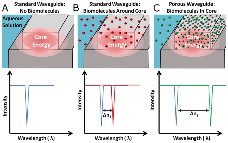
(a) Traditional on chip optical biosensors rely on biomolecules interacting with a traveling waves evanescent field instead of the much higher core energy. (b) When biomolecules are present, the optical path length increases and the resonance of a ring resonator red shifts. (c) Here we demonstrate polymer devices where biomolecules more strongly interact with the core electromagnetic energy by directly entering pores in the resonator. Because of increased interaction with the electromagnetic energy, the resonance peak shifts further (Δn2 > Δn1).
At the other end of the spectrum, polymer optical biosensors offer low cost, simple fabrication, but suffer from lower sensitivities than silicon equivalents [10,12,13, 20–22]. Polymers are commercially available with a range of thermal, mechanical, and optical properties, and can be readily functionalized for the immobilization of biomolecular sensing agents [23]. Further, Polymer chemistry can be tuned to yield unique optical structures and properties that are difficult to fabricate with traditional silicon based techniques. Due to their cheap material and fabrication requirements polymer biosensors lend themselves well to being manufactured as one-use disposables. Because of this, problems with surface fouling due to repeated use can often be mitigated.
In this paper, we present a method of increasing the sensitivity of optically resonant polymer biosensors. Ring resonators are chosen for their relatively high Q factors and excellent ability to localize optical energy. By creating porous resonators, bioanalytes in the detection medium are enabled to interact with the core waveguide energy increasing the effect these molecules have on the devices resonance, and thus increasing the devices sensitivity, as illustrated in Fig. 1. The increase in sensitivity associated with added porosity stems from both an increase in the amount of bioanalyte allowed to interact with the modal energy as well as an increase in the average modal energy the bioanalytes can interact with. Together these effects allow for greater enhancements to sensitivity than a similar increase in surface area would if unaccompanied by the deeper access pores provide.
Figure 2 shows an example of a nanoporous polymer optofluidic device consisting of a ring resonator coupled to a bus waveguide. These devices are fabricated using imprint lithography, a unique blend of polymers, and a selective solvent. By using nanoporous materials, we are able to detect biomolecular interactions occurring throughout the core of the ring resonator, enabling a 40% increase in sensitivity. We demonstrate this technique using polystyrene nanoporous waveguides, which we combine with polymeric microfluidics to yield an optofluidic biosensor constructed of inexpensive polymers.
Fig. 2.
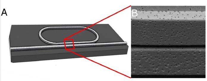
(a) An illustration of porous waveguides and a ring resonator show the underlying device structure. A ring resonator was chosen in order to increase sensitivity by further localizing light to a porous location. (b) A scanning electron micrograph (SEM) of two adjacent porous waveguides highlights how interactions can occur both around and in the waveguide core.
2. Methods
Figure 3 shows a schematic representation of the fabrication process. As detailed below, an imprint master was prepared using traditional photolithography and coated with an antistiction layer before embossing. Selected solvation was used to remove one polymer from a two-polymer system, and microfluidic channels were attached to the resonators to allow localization of target biomolecules. Optical excitation studies were then performed to determine changes in the resonance and sensitivity of devices as a function of added porosity.
Fig. 3.

A two step lithographic process was employed to create nanoporous waveguides. (a) First, an embossing master was created out of silicon oxide using standard photolithographic techniques and fluorine based etching. (b) Second, a custom polymer resist was spun onto a silicon oxide on silicon wafer, imprinted using the embossing master, and then developed using a select solvent.
2.1 Mode calculations and simulations
Lumerical FDTD Solutions software (Lumerical Solutions, Inc, Vancouver, British Columbia, Canada) was used to analyze mode profiles and ring resonators in order to determine the effective refractive indices of our waveguides as well as approximate resonator characteristics. Three dimensional calculations of mode profiles produced effective refractive indices for our waveguides which were then used to determine optimal waveguide cross-sections as well as approximate ring radii and coupling lengths.
2.2 Silicon master preparation
Hot embossing masters were fabricated from silicon wafers. A 2 µm film of undoped silicon oxide was deposited onto clean silicon wafers using plasma enhanced chemical vapor deposition. Wafers were then treated with P10 primer for ten seconds to promote photoresist adhesion, after which SPR 955 - 0.9 (MicroChem Corporation, Newton, MA, USA) positive photoresist was spun at 3000 rpm for 30 seconds. After a 90 second soft bake at 90 °C, wafers were patterned on an i-line autostepper, subjected to a post exposure bake of 90 seconds at 115 °C, and developed for one minute in AZ300-MIF alkaline developer. Patterned wafers were anisotropically etched on an Oxford PlasmaLab 80 + using fluorine based gas chemistry (50 sccm CHF3, 2 sccm O2, 50 mTorr, 200 W) to yield 1.1 µm deep features. After stripping residual photoresist, etched masters were cleaned for 10 minutes with oxygen plasma. This cleaning process was used to ensure uniformity and stability of the anti-stiction coating ((1H,1H,2H,2H-perfluorooctyl)trichlorosilane, FOTS) which was deposited using molecular vapor deposition in order to prevent stiction between the silicon master and the polymer substrate during imprint.
2.3 Substrate preparation
A 3 µm film of undoped silicon oxide was vapor deposited onto clean silicon wafers to serve as a lower cladding material beneath the polymer waveguides and ring resonators. An 80:20 weight ratio blend of polystyrene (PS, Mw 13,502, Pressure Chemical Company, Pittsburgh, PA, USA) and polymethylmethacrylate (PMMA, Mw 15,000, Scientific Polymer Products, Ontario, NY, USA) was dissolved to 5% by weight in tetrahydrofuran. After filtering through a 0.22 µm nylon syringe filter, the polymer blend was spun on wafers for 30 seconds at 2000 rpm, followed by curing at 145 °C for five minutes to drive off residual solvent.
2.4 Hot embossing
Polymer waveguides and ring resonators were formed using nanoimprint lithography (Nanonex, Monmouth Junction, NJ, USA). Polymer substrates were brought into contact with silicon masters and degassed for 2 minutes during the chamber pump down. Substrates and masters were heated to 130 °C and pressurized to 120 psi to precondition the polymer, followed by embossing at 140 °C and 500 psi for four minutes. In agreement with the previous literature, because of the aspect ratio between the waveguide structures and the thin polymer film, for many patterns higher pressure was needed than when imprinting other features [12,13]. Substrates were cleaved by marking the edge of the wafer onto which the polymer waveguides had been embossed using a diamond scribe, and carefully snapping the wafer along one of its crystal planes. Scanning electron microscopy revealed that this technique yielded smooth polymeric end facets, free of debris or roughness (see Fig. 5b ). On average this technique allowed us to yield approximately six working devices from a four inch wafer imprinted with a total of nine devices.
Fig. 5.
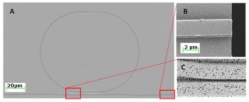
(a) A scanning electron micrograph shows the complete ring resonator and its relative dimensions. (b) The end facets generated by our cleave and snap technique show how precisely the waveguides can be fractured.(c) An SEM illustrates the smallest feature size on our devices and show how the ring and bus waveguide smoothly come to within a few hundred nanometers of each other. Further, pores developed with DMSO are also shown here.
2.5 Nanopore development
Nanopores were introduced to the embossed optical structures by selectively developing out PMMA from the PMMA-PS composite devices. Ring resonators were covered in a droplet of dimethylsulfoxide (DMSO) for 2 hours, followed by rinsing in water and drying under filtered air. Because of the different solubility characteristics of PS and PMMA in DMSO only PMMA is removed this way leaving a porous polystyrene waveguide behind. Further, by localizing pores to only the resonators, and not the entire bus waveguide, transmission loses were significantly reduced. If pores were created by placing the devices in bulk DMSO solutions, pores developed much faster (2-10minutes), likely attributed to the better mass transport of the larger solvent. For longer times in DMSO the waveguide structures delaminate from the underlying silicon oxide. Additionally, development based on oxygen plasma was also investigated. By etching devices in oxygen plasma for 3 to 5 minutes PMMA can be removed from PS due to its higher reactivity with the oxygen species.
2.6 Surface analysis
The morphology of nanoporous waveguides and resonators, as well as the integrity of embossed structures, were observed using scanning electron microscopy. A thin gold layer (<5 nm) was sputtered onto the waveguide structures prior to imaging and scanning electron microscopy was performed at energies between 1keV and 2 keV. Refractive indices of the polymers were determined on a Woollam Spectroscopic Ellipsometer scanning at angles of incidence ranging from 65° to 75°, varying wavelength from 3,000 to 10,000 Å. Film thickness was characterized using a FilMetrics Optical Film Measurement System (Filmetrics, Inc., San Diego, CA). Freeze fracture techniques in liquid nitrogen were also employed in order to determine the extent and depth of porosity.
2.7 Microfluidic channels
Microfluidic masters were fabricated using standard photolithography techniques and SU-8. Poly (dimethylsiloxane) (PDMS, Ellsworth Adhesives) molds were produced using soft lithography and aligned to our optical chips using a set of translational stages and a microscope. Holders for the device were laser cut out of Plexiglas and fit around the fluidic and optical layers as shown in Fig. 4 . This technique was used over traditional PDMS-glass oxygen plasma bonding because of the effect oxygen plasma has on our composite material. Holes punched through the PDMS layer were fit with small metal interconnects and tubes were attached allowing flow to be induced both with a syringe manually or with a syringe pump for regulated flow velocities.
Fig. 4.
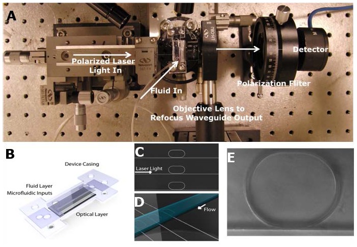
(a) An illustration of the experimental setup is shown. Polarized laser light is sent through a lensed fiber and coupled into the waveguide. The waveguide is offset by 3mm to prohibit scattered light from reaching the detector and outcoming light is refocused through an objective lens, put through a polarization filter, and then reaches a photodetector. (b) Optical and microfluidic devices are shown aligned and sandwiched between two Plexiglas device holders. The final assembly is screwed closed forming a tight seal around our microfluidic channels. Illustrations show the concentration of the light (c) and fluid (d) are localized to one small area over the resonator. (e) Shows a ring resonator imaged through the device and covered in aqueous solution.
2.8 Optical excitation
An Ando AQ4321D laser source (tunable between 1520 and 1620 nm) was used to couple light into polymeric waveguides as in previous work by our group [5]. Both the fiber and the chip are mounted on 3-axis stages to ensure accurate alignment. The input and output facets of the waveguide are shifted by 3 mm to prevent detection of scattered light. Light that passes through the waveguide is collected and collimated, then passed through a polarizer to select only the TM mode, before reaching the photodetector, as shown in Fig. 4a.
2.9 Sensitivity measurements
Resonator sensitivity was determined by immersing the waveguides in an aqueous cladding solution of varying amounts of glucose. Solution refractive indices were determined using a refractometer. Glucose concentrations were chosen in order to make sure resonant peak shift from one solution to another didn’t exceed the free spectral range of the devices in order to make sure peaks could be identified. Specifically, five glucose solutions were chosen at approximately 0, 5, 10, 15, and 20% to satisfy this requirement and because of availability. Solutions were measured before each experiment to confirm their refractive index.
3. Results and discussion
3.1 Lumerical FDTD simulations
The results of our FDTD simulations indicate that polystyrene waveguides with dimensions 1 µm in height by 2.5 µm in width support both one TE and one TM mode. Because of limitations from the fabrication techniques used we were only able to place our resonators within 250 to 400 nm of the bus waveguide that evanescently coupled into them. At this spacing, our simulations determined that the racetrack resonators would achieve the highest energy storage with a coupling length of around 20 to 30 µm. Comparing both scattering and bending losses we were able to determine that radii less than 20 µm had prohibitively high bending loses and that increases beyond radii of approximately 60 µm only seemed to increasing scattering losses. This information was used to guide the fabrication of the resonators with the goal of obtaining reasonable Q factors.
3.2 Porous resonator fabrication
Resonators were place between 250 and 400 nm from our waveguide, the closest we were able to achieve with the i-line stepper we used. We produced racetrack resonators of sizes ranging from 35 µm radii and 20 µm coupling lengths to 65 µm radii and 30 µm coupling lengths. By tuning parameters such as the ratio of the two polymers we were able to observe differences in resulting pore sizes. DMSO selectively removed PMMA from polystyrene without adversely affecting the polystyrene waveguide structure (Fig. 5). Additionally, oxygen plasma etching created even more porous structures, but was difficult to isolate to only the ring region resulting in devices which scattered too much to optically excite and measure (Fig. 6 ). Using a cleave and snap technique we were able to repeatedly generate smooth edges for light coupling with no deformation or debris. Porosity in solvent generated waveguides and resonators was approximately 9-10% of their surface area with pore diameters on the order of 60 to 120 nm and depths on the order of a few hundred nanometers. In general, there was little interconnectedness between pores in these waveguides. Because polystyrene has a contact angle less than 90° [24], we suspect the pores are wetting, and that aqueous solutions are capable of penetrating into the structure.
Fig. 6.
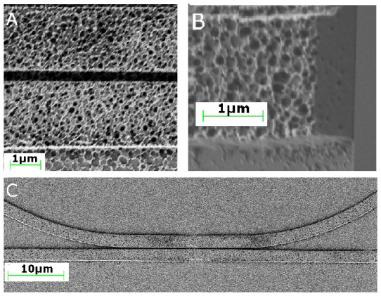
(a.) A scanning electron micrograph shows a ring resonator made porous using oxygen plasma. (b) An end facet which was freeze fractured shows pores running throughout the waveguide structure. (c) A racetrack resonator and waveguide are shown separated by approximately 300 nm, the smallest top down fabricated feature on the device.
3.3 Optical excitation and resonance measurements
A typical spectrum from the resonators is shown in Fig. 7 . The cladding liquid here is water and approximately 1mW of laser power is coupled into the waveguide. After loses from coupling and scattering approximately 40-100 microwatts of power are collected at the detector. Depending on the exact fabrication of the resonator and any defects in it, we observed extinctions between 3 and 15dB at the resonant wavelength and Q-factors between 1000 and 3000. In general, we observed resonators with larger radii tended to outperform smaller ones, a factor we attributed to high bending losses due to the relatively small index difference between polystyrene and water. Resonance peaks were fit with Lorentzian functions in order to determine their location and full width half max.
Fig. 7.

A typical output spectrum of a porous resonator is shown. The free spectral range of the devices is approximately 2.8 nm, the quality factors range from 1000 to 3000, and on resonance wavelengths have extinctions between 3 and 15 dB.
3.4 Resonance shift as a function of porosity
As DMSO is allowed to dissolve PMMA out from our waveguide we observe a blue shift in resonance corresponding to this loss of material. Using this type of measurement we can observe pores being added to our material simply through measurements of the optical resonance of the devices. Figure 8 shows measurements taken as a device was exposed to DMSO. After each exposure to DMSO the resonators were rinsed with water and dry air before the next measurement was taken. These rinsing and drying steps are important because the refractive index of DMSO is approximately 1.48, and when the porous resonator is covered with and filled by DMSO the resonant peaks red shift. As the DMSO evaporates the resonant peaks blue shift back and reach a final stable point once the DMSO is no longer present.
Fig. 8.
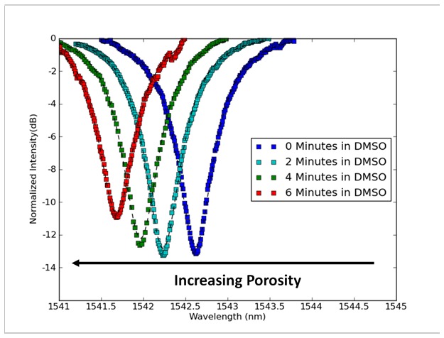
As the porosity of a ring resonator increases its resonance blue shifts. This change corresponds with decreasing mass and a shorter optical path and is a good indicator that pores are being generated. Measurements of resonance were taken with the resonator immersed in water at all four timepoints, and conditions were controlled so the only change was the addition of pores.
3.5 Effect of porosity on sensitivity
Figure 9 shows resonances both before pores were added and after in a single device as well as SEMs of a nonporous device and after pores are added. A resonant peak is plotted at five different glucose concentrations for each resonator. Note that as the index of the cladding solution increases the resonant condition red-shifts, which corresponds with the longer optical path. This result agrees with Fig. 8, where a blue-shift was observed due to a shortening of the optical path associated with the addition of pores. Due to increased interaction between the aqueous sample solution and the waveguide’s core energy the change in resonance is greater in the porous device. Additionally, Fig. 10 compares the sensitivity of nonporous and porous resonators, showing a 42% increase in resonator sensitivity. Standard error is used to show inter device variability, which is significantly higher for the porous resonators compared to the nonporous, a characteristic we attribute to different porosity arising during fabrication. Both sets of data were fit with a linear regression running through the origin and sensitivities of 66.15 and 94.05 were determined. The nonporous and porous resonator sensitivities have coefficient of determination (R2) values of 0.995 and 0.968, respectively, both indicating a good fit.
Fig. 9.

The resonance shift of nonporous (a) polymer resonators is compared to their (b) porous counterparts. Measurements are taken at five different concentrations of glucose between 0 and 20 percent. As the refractive index of the cladding solution increases, a corresponding red shift is seen in the resonance condition of the rings. Because of increased bioanalyte electromagnetic energy interactions occurring in the porous waveguide the sensitivity of the device is significantly increased, and further shifts can be observed in (b) than (a). SEMs of a waveguide without pores (c) and of the waveguide after pores (d) are added are also shown.
Fig. 10.

The sensitivity of a porous resonator is plotted against that of a nonporous resonator. An increase in over 40% sensitivity can be seen. The first data point appears at 0 corresponding to the resonator immersed in water.
4. Conclusions
In this work we have shown how porous polymer waveguides can be fabricated using nanoimprint lithography and selective solvents. The porous structures created provide higher sensitivity than their nonporous counterparts and the modification can be performed in only one additional step using only a solvent. This modification can be made prior to functionalization and fits naturally into the creation of ring resonator biosensors. Additionally other changes could be made to further enhance the sensitivity of porous waveguides. One example is the use of wetting agents that could allow bioanalytes to penetrate deeper into the porous waveguide structure and further increase sensitivity. A second example involves allowing bioanalyte solution to dissolve on the waveguide, concentrating the molecules of interest into the pores, where they would be capable of causing a greater change in sensitivity. One limitation in this work is the lack of quantitative biomolecular sensing studies. In future work we plan on functionalizing these porous waveguides for certain biomarkers and determining how their porous nature effects these detection reactions.
The work presented here only shows a simple application of how two-polymer systems can be used to create interesting nanostructures for optics. Here the polymers are mixed in suspension and allowed to phase separate into random arrangements. In theory, it's possible to imagine that by creating diblock copolymers or other similar systems that two polymers could be caused to assemble into long-range ordered structures [25]. These nanostructures could not only allow for increased sensitivity in ring structures but could also potentially be used to create interesting optical materials, including self-assembled photonic crystals.
We have shown that by using simple polymer techniques the sensitivity of optical resonators can be increased by over 40%. While the sensitivity of polymer devices is generally lower than traditional silicon devices these porous additions can provide polymer ring resonators an advantage. This increase in sensitivity combined with the simple fabrication and low cost associated with polymers can provide a distinct advantage to these devices and a simple way to make highly sensitive inexpensive biosensors.
Acknowledgements
This material is based upon work supported by the National Science Foundation Graduate Research Fellowship under Grant No. DGE-0707428. Additional support for this work was provided by the National Institutes of Health - National Institute of Biomedical Imaging and Bioengineering (NIH-NIBIB) under grant number R21EB007031. This work made use of STC shared experimental facilities supported by the National Science Foundation under Agreement No. ECS-9876771. The authors gratefully acknowledge Michael Mak for assistance in mode calculations, Sudeep Mandal for assistance in light coupling experiments, Xavier Serey for help with resonator simulations, and all three for numerous technical discussions.
References and links
- 1.Cooper M. A., “Label-free screening of bio-molecular interactions,” Anal. Bioanal. Chem. 377(5), 834–842 (2003). 10.1007/s00216-003-2111-y [DOI] [PubMed] [Google Scholar]
- 2.Erickson D., Mandal S., Yang A. H. J., Cordovez B., “Nanobiosensors: optofluidic, electrical and mechanical approaches to biomolecular detection at the nanoscale,” Microfluid. Nanofluid. 4(1-2), 33–52 (2008). 10.1007/s10404-007-0198-8 [DOI] [PMC free article] [PubMed] [Google Scholar]
- 3.Anker J. N., Hall W. P., Lyandres O., Shah N. C., Zhao J., Van Duyne R. P., “Biosensing with plasmonic nanosensors,” Nat. Mater. 7(6), 442–453 (2008). 10.1038/nmat2162 [DOI] [PubMed] [Google Scholar]
- 4.Vollmer F., Arnold S., “Whispering-gallery-mode biosensing: label-free detection down to single molecules,” Nat. Methods 5(7), 591–596 (2008). 10.1038/nmeth.1221 [DOI] [PubMed] [Google Scholar]
- 5.Mandal S., Erickson D., “Nanoscale Optofluidic Sensor Arrays,” Opt. Express 16(3), 1623–1631 (2008). 10.1364/OE.16.001623 [DOI] [PMC free article] [PubMed] [Google Scholar]
- 6.Daniels J. S., Pourmand N., “Label-free impedance biosensors: Opportunities and challenges,” Electroanalysis 19(12), 1239–1257 (2007). 10.1002/elan.200603855 [DOI] [PMC free article] [PubMed] [Google Scholar]
- 7.Länge K., Rapp B. E., Rapp M., “Surface acoustic wave biosensors: a review,” Anal. Bioanal. Chem. 391(5), 1509–1519 (2008). 10.1007/s00216-008-1911-5 [DOI] [PubMed] [Google Scholar]
- 8.Yariv A., “Universal relations for coupling of optical power between microresonators and dielectric waveguides,” Electron. Lett. 36(4), 321–322 (2000). 10.1049/el:20000340 [DOI] [Google Scholar]
- 9.Yariv A., “Critical coupling and its control in optical waveguide-ring resonator systems,” IEEE Photon. Technol. Lett. 14(4), 483–485 (2002). 10.1109/68.992585 [DOI] [Google Scholar]
- 10.Seo B. J., Kim S., Fetterman H., Steier W., Jin D., Dinu R., “Design of ring resonators using electro-optic polymer waveguides,” J. Phys. Chem. C 112(21), 7953–7958 (2008). 10.1021/jp711914a [DOI] [Google Scholar]
- 11.Xu D. X., Densmore A., Delâge A., Waldron P., McKinnon R., Janz S., Lapointe J., Lopinski G., Mischki T., Post E., Cheben P., Schmid J. H., “Folded cavity SOI microring sensors for high sensitivity and real time measurement of biomolecular binding,” Opt. Express 16(19), 15137–15148 (2008). 10.1364/OE.16.015137 [DOI] [PubMed] [Google Scholar]
- 12.Chao C. Y., Guo L. J., “Polymer microring resonators fabricated by nanoimprint technique,” J. Vac. Sci. Technol. B 20(6), 2862–2866 (2002). 10.1116/1.1521729 [DOI] [Google Scholar]
- 13.Chao C. Y., Fung W., Guo L. J., “Polymer microring resonators for biochemical sensing applications,” IEEE J. Sel. Top. Quantum Electron. 12(1), 134–142 (2006). 10.1109/JSTQE.2005.862945 [DOI] [Google Scholar]
- 14.Mandal S., Goddard J. M., Erickson D., “A multiplexed optofluidic biomolecular sensor for low mass detection,” Lab Chip 9(20), 2924–2932 (2009). 10.1039/b907826f [DOI] [PubMed] [Google Scholar]
- 15.Martin A. L., Armani D. K., Yang L., Vahala K. J., “Replica-molded high-Q polymer microresonators,” Opt. Lett. 29(6), 533–535 (2004). 10.1364/OL.29.000533 [DOI] [PubMed] [Google Scholar]
- 16.Myers F. B., Lee L. P., “Innovations in optical microfluidic technologies for point-of-care diagnostics,” Lab Chip 8(12), 2015–2031 (2008). 10.1039/b812343h [DOI] [PubMed] [Google Scholar]
- 17.De Vos K., Girones J., Popelka S., Schacht E., Baets R., Bienstman P., “SOI optical microring resonator with poly(ethylene glycol) polymer brush for label-free biosensor applications,” Biosens. Bioelectron. 24(8), 2528–2533 (2009). 10.1016/j.bios.2009.01.009 [DOI] [PubMed] [Google Scholar]
- 18.Barrios C. A., “Optical Slot-Waveguide Based Biochemical Sensors,” Sensors (Basel Switzerland) 9(6), 4751–4765 (2009). 10.3390/s90604751 [DOI] [PMC free article] [PubMed] [Google Scholar]
- 19.Barrios C. A., Gylfason K. B., Sánchez B., Griol A., Sohlström H., Holgado M., Casquel R., “Slot-waveguide biochemical sensor,” Opt. Lett. 32(21), 3080–3082 (2007). 10.1364/OL.32.003080 [DOI] [PubMed] [Google Scholar]
- 20.Rabus D. G., Bruendel M., Ichihashi Y., Welle A., Seger R. A., Isaacson M., “A bio-fluidic-photonic platform based on deep UV modification of polymers,” IEEE J. Sel. Top. Quantum Electron. 13(2), 214–222 (2007). 10.1109/JSTQE.2007.892073 [DOI] [Google Scholar]
- 21.Kehagias N., Zankovych S., Goldschmidt A., Kian R., Zelsmann M., Torres C. M. Sotomayor, Pfeiffer K., Ahrens G., Gruetzner G., “Embedded polymer waveguides: design and fabrication approaches,” Superlattices Microstruct. 36(1-3), 201–210 (2004). 10.1016/j.spmi.2004.08.005 [DOI] [Google Scholar]
- 22.Xu F., Datta P., Wang H., Gurung S., Hashimoto M., Wei S., Goettert J., McCarley R. L., Soper S. A., “Polymer microfluidic chips with integrated waveguides for reading microarrays,” Anal. Chem. 79(23), 9007–9013 (2007). 10.1021/ac7016597 [DOI] [PMC free article] [PubMed] [Google Scholar]
- 23.Goddard J. M., Hotchkiss J. H., “Polymer surface modification for the attachment of bioactive compounds,” Prog. Polym. Sci. 32(7), 698–725 (2007). 10.1016/j.progpolymsci.2007.04.002 [DOI] [Google Scholar]
- 24.Li Y., Pham J. Q., Johnston K. P., Green P. F., “Contact Angle of Water on Polystyrene Thin Films: Effects of CO(2) Environment and Film Thickness,” Langmuir 23(19), 9785–9793 (2007). 10.1021/la0636311 [DOI] [PubMed] [Google Scholar]
- 25.Mahajan S., Renker S., Simon P. F. W., Gutmann J. S., Jain A., Gruner S. M., Fetters L. J., Coates G. W., Wiesner U., “Synthesis and characterization of amphiphilic poly(ethylene oxide)-block-poly(hexyl methacrylate) copolymers,” Macromol. Chem. Phys. 204(8), 1047–1055 (2003). 10.1002/macp.200390084 [DOI] [Google Scholar]


