Abstract
This paper reports the effect of precursor concentration, growth temperature, and growth time on the size and density of ZnO nanowire arrays (ZNAs). The well-aligned ZNAs were grown on indium tin oxide substrate using a facile chemical bath deposition method. The results showed that the ZnO nanowires could be tailored to the desired sizes with a simple variation of the growth parameters. Optical transmission spectra revealed a sufficient transparency of the ZNAs, qualifying them for photovoltaic and other optoelectronic applications. An inverted hybrid solar cell was fabricated using the ZNAs as the electron collecting layer, and the solar cell exhibited a power conversion efficiency of 0.91%.
Keywords: ZnO nanowire arrays, Chemical bath deposition, Optical transmission, Hybrid solar cell
Background
As an important wide-bandgap semiconductor, ZnO possesses remarkable optical, electrical, and optoelectronic properties, thus being of immense research interest [1-4]. Recently, well-aligned ZnO nanowire or nanorod arrays have been extensively studied as a promising candidate for applications in electroluminescent devices [5,6], field emission devices [7], solar cells [8-14], nanogenerators [15-17], and chemical sensors [18-20].
To grow well-aligned ZnO nanowire arrays (ZNAs), various synthesis methods have been utilized, such as thermal evaporation [7], chemical vapor transport and condensation [18], and vapor–liquid-solid growth [20]; the complex process, sophisticated equipment, and high temperatures make it hard to use them on a wide range of substrates. In contrast, the chemical bath deposition method shows its great advantages due to its much easier operation, very low temperature (≤ 95°C) growth, high potential for scale-up, and low-cost. The facile and low-temperature growths favor the applications of well-aligned ZNAs as electroluminescent diodes and hybrid solar cells [8-10]. Previous reports [21,22] indicate that the sizes (diameter and length) of ZnO nanowires or nanorods play an important role on the performance of building ZNA hybrid solar cells. In light of our experimental observations, several factors, including concentration of precursors, growth temperature, and growth time, had great effect on the sizes and density of well-aligned ZNAs grown via the chemical bath deposition method. However, up to now, only a few works on size-controlled and transparent well-aligned ZNAs are available [21,23].
In this work, we present size-controlled and transparent ZNAs by a facile chemical bath deposition method. It is shown that the nanowires can be tailored to the desired sizes with a simple variation of the growth parameters. The optical transmission of the obtained well-aligned ZNAs in the visible wavelength region was also discussed. Exemplarily, a hybrid solar cell was constructed and fabricated, consisting of the as-prepared ZNAs and polymer hybrid bulk heterojunction architecture.
Methods
Materials and substrates
Regioregular poly(3-hexylthiophene-2,5-diyl) (P3HT, 99.5%) and (6,6)-phenyl-C61-butyric acid methyl ester (PCBM, 99.5%) were purchased from Lumtec (Hsin-Chu, Taiwan) and used as received. Other chemicals (Kelong Chemical Agent, Chengdu, China) used in our experiments were of analytical reagent grade without further purification. All the aqueous solutions were prepared using distilled water (resistivity = 18.2 MΩ cm). The indium tin oxide (ITO)-coated glasses (10 Ω/sq) were used as the substrate and first cleaned by ultrasonic agitation in detergent, then deionized water, acetone, and ethanol, successively. The cleaned substrates were then blown dry using nitrogen gas and treated with O2 plasma for 5 min.
Preparation of ZNAs
ZNAs were prepared by the following two-step process, and the growth of the ZNAs was conducted following our previous work [24,25]. Briefly, zinc acetate dehydrate (Zn(CH3COO)2·2H2O) was dissolved in ethanol with a concentration of 5 mM. A droplet of the solution was coated onto treated ITO substrates, rinsed with clean ethanol after 10 s, and then blown dry with a stream of nitrogen gas. This coating step was repeated several times. The coated substrates were dried at room temperature and then annealed at 350°C for 20 min in air to yield the multilayers of ZnO seed. The zinc acetate deposition and decomposition procedure were carried out twice to ensure a complete and uniform coverage of ZnO seeds.
Then, the ZNAs were grown in 200 mL of equimolar aqueous solution of Zn(NO3)2·6H2O and hexamethylenetetramine (C6H12N4) in a conventional reaction flask. The ZnO seed layer-coated ITO substrate was immersed into the aqueous solution upside-down in the flask; the pH value of the growth solution was approximately 6.0 by adding aqueous ammonia. Various growth parameters such as concentration of precursors, growth temperature, and growth time were used in our experiments. Table 1 summarizes major experiments carried out in this work. After growth, the substrates were removed from the solution, rinsed with deionized water, and dried at 50°C in air.
Table 1.
Growth parameters of ZnO nanowire arrays
| Sample | Growth temperature (°C) | Growth time (h) | Concentration of precursors (M) |
|---|---|---|---|
| Sample A |
73 |
2 |
0.025 |
| Sample B |
83 |
2 |
0.025 |
| Sample C |
93 |
2 |
0.025 |
| Sample D |
93 |
1 |
0.025 |
| Sample E |
93 |
3 |
0.025 |
| Sample F |
93 |
4 |
0.025 |
| Sample G |
93 |
2 |
0.01 |
| Sample H |
93 |
2 |
0.05 |
| Sample I | 93 | 2 | 0.1 |
Preparation of ZNA/polymer hybrid solar cell
A hybrid solar cell was fabricated using the following procedure. The organic layers consisted of P3HT:PCBM (1:1 by weight ratio) were spin-coated on the top of sample C from a chlorobenzene solution with a concentration of 30 mg/ml in air, then annealed at 110°C for 15 min under vacuum (≤133 Pa). The 3-nm-thick MoO3 was deposited on the P3HT:PCBM layers under a pressure of 3 × 10⁻³ Pa as a buffer layer [24], followed by the deposition of 200-nm-thick Ag electrodes through a shadow mask.
Characterization
The morphology of as-grown ZNAs was analyzed using a field-emission scanning electron microscope (FESEM, Hitachi S-4800, Chiyoda-ku, Japan); X-ray diffractometry (XRD) data were obtained on a Philips X'pert Pro MPD diffractometer (CuKα radiation, λ = 1.54056 Å, Amsterdam, The Netherlands). Optical transmission was measured by a UV–vis spectrophotometer (SHIMADZU UV1700, Kyoto, Japan). The current–voltage characteristics of as-prepared solar cells in the dark and under illumination were recorded with a Keithley 4200 programmable voltage–current source (Cleveland, OH, USA) [26-28]. A solar simulator equipped with a xenon lamp with an illumination power of 500 W (CHF-XM35, Beijing Trusttech Co. Ltd., Beijing, China) was used as the light source. All measurements were performed under ambient conditions without device encapsulation.
Results and discussion
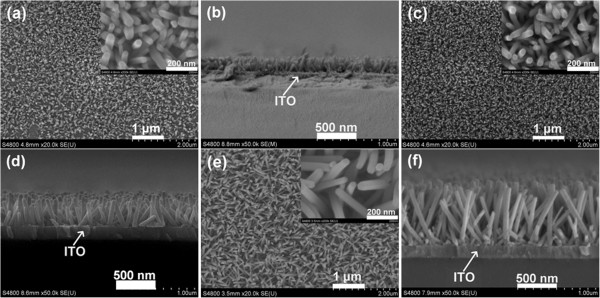
In this study, we found that the different growth temperatures strongly influenced the nanowire length and density of ZNAs. Figure 1 shows the top-view, high-magnification (shown in the insets), and cross-sectional FESEM images of samples A, B, and C. There are only wirelike features with a hexagonal cross section for all samples, which are aligned in a dense array approximately perpendicular to the substrate surface. The ZNAs uniformly covered the entire substrate surface based on the FESEM result. The mean values of the nanowire dimension and array density for samples A, B, and C were estimated from a statistical evaluation of FESEM images and are summarized in Table 2. We note that with the enhancement of growth temperature, both the average length and array density obviously increase, and the average diameter of nanowires almost displays no change.
Figure 1.
FESEM images of samples (a, b) A, (c, d) B, and (e, f) C. (a), (c), and (e) correspond to top views. (b), (d), and (f) correspond to cross-sectional views. The insets show high-magnification FESEM images.
Table 2.
Mean values of the nanowire diameter, length, and array density of the samples
| Sample | Diameter (nm) | Length (nm) | Density (×109wires/cm2) |
|---|---|---|---|
| Sample A |
30 |
190 |
11.0 |
| Sample B |
35 |
340 |
18.0 |
| Sample C |
35 |
750 |
19.2 |
| Sample D |
20 |
200 |
18.0 |
| Sample E |
45 |
1,000 |
19.8 |
| Sample F |
50 |
1,000 |
20.4 |
| Sample G |
30 |
500 |
10.4 |
| Sample H |
40 |
850 |
21.6 |
| Sample I | 200 | 950 | 4.8 |
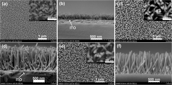
The effect of the growth time on the morphology and density of ZNAs was also investigated, as shown in Figure 2. It can be seen that the highly uniform and densely packed arrays of ZnO nanowires are successfully formed for samples D, E, and F. The mean values of the nanowire dimension and array density for samples D, E, and F are also summarized in Table 2. Comparing the average length, diameter, and array density among samples D, C, E and F, respectively, it can be seen that both the average diameter and array density slowly increase with elongating growth time. The average length rapidly increases as the growth time elongates from 1 to 3 h. However, further elongating the growth time, the average length shows no change.
Figure 2.
FESEM images of samples (a, b) D, (c, d) E, and (e, f) F. (a), (c), and (e) correspond to top views. (b), (d), and (f) correspond to cross-sectional views. The insets show high-magnification SEM images.
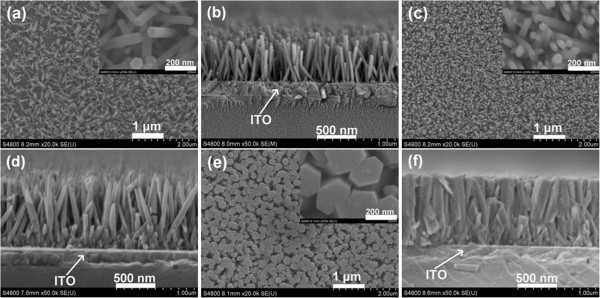
Figure 3 shows top-view, high-magnification (shown in the insets), and cross-sectional FESEM images of samples G, H, and I. The results reveal that well-aligned ZNAs are also obviously formed for samples G, H, and I. Also, the mean values of the nanowire dimension and array density for samples G, H, and I are summarized in Table 2. It can be seen that both the average diameter and length of the nanowires increase with the increased concentration of precursors from 0.01 to 0.1 M, as seen in samples G, C, H, and I in Table 2. The array density rapidly increases as the concentration of precursors ranged from 0.01 to 0.05 M. However, further increasing the concentration of precursors up to 0.1 M, the array density of ZNAs sharply decreases, which is attributed to the average diameter of the nanowires that becomes too large.
Figure 3.
FESEM images of samples (a, b) G, (c, d) H, and (e, f) I. (a), (c), and (e) correspond to top views. (b), (d), and (f) correspond to cross-sectional views. The insets show high-magnification SEM images.
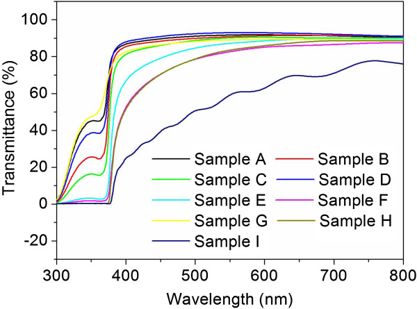
The optical transparency of all samples fabricated on ITO substrates was investigated. Figure 4 shows the optical transmittance spectra of samples A to I. With the exception of sample I, all of the samples show good optical transparency in the visible spectral range, with a transmittance above 80%. However, sample I displays a lower transmittance over a broad range of wavelengths as compared to other samples. This was due to the increase in light scattering from the large diameter of ZnO nanowires in sample I, which is consistent with the FESEM results.
Figure 4.
Optical transmittance spectra of samples A to I.
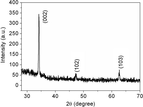
Figure 5 shows the XRD patterns of sample C. The XRD analysis reveals that all of the diffraction peaks of ZNAs can be indexed as those from the known wurtzite-structured (hexagonal) ZnO (JCPDS card no. 36–1451) and the (002) diffraction peak exhibits a substantially greater intensity. The result further demonstrates that as-grown ZNAs are much better aligned on the substrate and the nanowires exhibit preferred growth along the (0001) direction.
Figure 5.
XRD pattern of sample C.
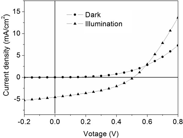
Finally, to testify the application of ZNAs for optoelectronic application, a hybrid solar cell (HSC) was built using sample C with a structure of sample C/P3HT:PCBM/MoO3/Ag. Figure 6 shows the typical current density-voltage (J-V) characteristics of the HSC in the dark and under AM 1.5 illumination with a light intensity of about 100 mW/cm2. The device exhibits an open-circuit voltage of 0.51 V, a short-circuit current of 4.53 mA/cm2, a fill factor of 39%, and a power conversion efficiency of 0.91%.
Figure 6.
J-V characteristics of sample C/P3HT:PCBM/MoO3/Ag solar cell in the dark and under AM 1.5 illumination. The light intensity is 100 mW/cm2.
Conclusions
In summary, well-aligned ZNAs were grown on ITO substrates by a facile chemical bath deposition method. Size-selected ZnO nanowires were achieved by changing the precursor concentration, growth temperature, and growth time. The well-aligned ZNAs showed good optical transparency in the visible spectral range, and the nanowires exhibited an excellent crystal quality. A hybrid solar cell composed of the investigated ZNAs with a reasonable power conversion efficiency were realized. This work will be beneficial to develop large-area, low-cost, and high-quality ZNA-based optoelectronic devices in the near future.
Competing interests
The authors declare that they have no competing interests.
Authors’ contributions
JSY is the primary author and participated in designing the experiments, experiment analysis and interpretation of data, and language modification. ZLY carried out the experiments, characterization, and acquisition of data. SJH and ZM are the investigators who helped in the analysis and interpretation of data, drafting of the manuscript, and revisions. All authors read and approved the final manuscript.
Contributor Information
Junsheng Yu, Email: jsyu@uestc.edu.cn.
Zhaolin Yuan, Email: yuanzhaolin98@yahoo.com.cn.
Shijiao Han, Email: hanshijiao@outlook.com.
Zhu Ma, Email: deve198509@163.com.
Acknowledgments
This work was partially supported by the National Natural Science Foundation of China (NSFC) via no. 61177032, the Foundation for Innovation Groups of NSFC via no. 61021061, the Fundamental Research Funds for the Central Universities (grant no. ZYGX2010Z004), SRF for ROCS, SEM (grant no. GGRYJJ08-05), and Doctoral Fund of Ministry of Education of China (grant no. 20090185110020).
References
- Pauzauskie PJ, Yang PD. Nanowire photonics. Materialstoday. 2006;9:36. [Google Scholar]
- Gopikrishnan R, Zhang K, Ravichandran P, Baluchamy S, Ramesh V, Biradar S, Ramesh P, Pradhan J, Hall JC, Pradhan AK, Ramesh GT. Synthesis, characterization and biocompatibility studies of zinc oxide (ZnO) nanorods for biomedical application. Nano-Micro Lett. 2010;2:27. [Google Scholar]
- Hossain MF, Takahashi T, Takakazu T. Novel micro-ring structured ZnO photoelectrode for dye-sensitized solar cell. Nano-Micro Lett. 2010;2:53. [Google Scholar]
- Zhang YF, Zhang B, Hu NT, Wang YF, Wang Z, Wang Y, Kong ES. Poly(glycidyl methacrylates)-grafted zinc oxide nanowire by surface-initiated atom transfer radical poly- merization. Nano-Micro Lett. 2010;2:285. [Google Scholar]
- Konenkamp R, Word RC, Schlegel C. Vertical nanowire light-emitting diode. Appl Phys Lett. 2004;85:6004. doi: 10.1063/1.1836873. [DOI] [Google Scholar]
- Park WI, Yi GC. Electroluminescence in n-ZnO nanorod arrays vertically grown on p-GaN. Adv Mater. 2004;16:87. doi: 10.1002/adma.200305729. [DOI] [Google Scholar]
- Li LM, Du ZF, Li CC, Zhang J, Wang TH. Ultralow threshold field emission from ZnO nanorod arrays grown on ZnO film at low temperature. Nanotechnology. 2007;18:355606. doi: 10.1088/0957-4484/18/35/355606. [DOI] [Google Scholar]
- Olson DC, Lee YJ, White MS, Kopidakis N, Shaheen SE, Ginley DS, Voigt JA, Hsu JWP. Effect of polymer processing on the performance of poly(3-hexylthiophene)/ZnO nanorod photovoltaic devices. J Phys Chem C. 2007;111:16640. doi: 10.1021/jp0757816. [DOI] [Google Scholar]
- Ravirajan P, Peiró AM, Nazeeruddin MK, Graetzel M, Bradley DDC, Durrant JR, Nelson J. Hybrid polymer/zinc oxide photovoltaic devices with vertically oriented ZnO nanorods and an amphiphilic molecular interface layer. J Phys Chem B. 2006;110:7635. doi: 10.1021/jp0571372. [DOI] [PubMed] [Google Scholar]
- Leschkies KS, Divakar R, Basu J, Enache-Pommer E, Boercker JE, Cater CB, Kortshagen UR, Norris DJ, Aydil ES. Photosensitization of ZnO nanowires with CdSe quantum dots for photovoltaic devices. Nano Lett. 2007;7:1793. doi: 10.1021/nl070430o. [DOI] [PubMed] [Google Scholar]
- Hsu YF, Xi YY, Djurišić AB, Chan WK. ZnO nanorods for solar cells: hydrothermal growth versus vapor deposition. Appl Phys Lett. 2008;92:133507. doi: 10.1063/1.2906370. [DOI] [Google Scholar]
- Baxter JB, Aydi ES. Nanowire-based dye-sensitized solar cells. Appl Phys Lett. 2005;86:053114. doi: 10.1063/1.1861510. [DOI] [Google Scholar]
- Yang WN, Wang FR, Chen SW, Jiang CH. Hydrothermal growth and application of ZnO nanowire films with ZnO and TiO2 buffer layers in dye-sensitized solar cells. Nanoscale Res Lett. 2009;4:1486. doi: 10.1007/s11671-009-9425-4. [DOI] [PMC free article] [PubMed] [Google Scholar]
- Law M, Greene LE, Johnson JC, Saykally R, Yang PD. Nanowire dye-sensitized solar cells. Nat Mater. 2005;4:455. doi: 10.1038/nmat1387. [DOI] [PubMed] [Google Scholar]
- Wang ZL, Song JH. Direct-current nanogenerator driven by ultrasonic waves. Science. 2006;312:242. doi: 10.1126/science.1124005. [DOI] [PubMed] [Google Scholar]
- Qin Y, Wang XD, Wang ZL. Microfibre-nanowire hybrid structure for energy scavenging. Nature. 2008;451:809. doi: 10.1038/nature06601. [DOI] [PubMed] [Google Scholar]
- Wang XD, Liu J, Song JH, Wang ZL. Integrated nanogenerators in biofluid. Nano Lett. 2007;7:2475. doi: 10.1021/nl0712567. [DOI] [PubMed] [Google Scholar]
- Wang XY, Wang YM, Åberg D, Erhart P, Misra N, Noy A, Hamza AV, Yang JH. Batteryless chemical detection with semiconductor nanowires. Adv Mater. 2011;23:117. doi: 10.1002/adma.201003221. [DOI] [PubMed] [Google Scholar]
- Wang XD, Summers CJ, Wang ZL. Large-scale hexagonal-patterned growth of aligned ZnO nanorods for nano-optoelectronics and nanosensor arrays. Nano Lett. 2004;4:423. doi: 10.1021/nl035102c. [DOI] [PubMed] [Google Scholar]
- Luo L, Sosnowchik BD, Lin L. Local vapor transport synthesis of zinc oxide nanowires for ultraviolet-enhanced gas sensing. Nanotechnology. 2010;21:495502. doi: 10.1088/0957-4484/21/49/495502. [DOI] [PubMed] [Google Scholar]
- Takanezawa K, Hirota K, Wei QS, Tajima K, Hashimoto K. Efficient charge collection with ZnO nanorod array in hybrid photovoltaic devices. J Phys Chem C. 2007;111:7218. [Google Scholar]
- Greene LE, Law M, Tan DH, Montano M, Goldberger J, Somorjai G, Yang P. General route to vertical ZnO nanowire arrays using textured ZnO seeds. Nano Lett. 2005;5:1231. doi: 10.1021/nl050788p. [DOI] [PubMed] [Google Scholar]
- Greene LE, Law M, Goldberger J, Kim F, Johnson JC, Zhang Y, Saykally RJ, Yang P. Low-temperature wafer-scale production of ZnO nanowire arrays. Angew Chem Int Ed. 2003;42:3031. doi: 10.1002/anie.200351461. [DOI] [PubMed] [Google Scholar]
- Yuan ZL, Yu JS, Wang NN, Jiang YD. Well-aligned ZnO nanorod arrays from diameter-controlled growth and their application in inverted polymer solar cell. J Mater Sci Mater Electron. 2011;22:1730. doi: 10.1007/s10854-011-0353-6. [DOI] [Google Scholar]
- Yuan ZL, Yu JS, Ma WM, Jiang YD. A photodiode with high rectification ratio based on well-aligned ZnO nanowire arrays and regioregular poly(3-hexylthiophene-2,5-diyl) hybrid heterojunction. Appl Phys A. 2012;106:511. doi: 10.1007/s00339-011-6756-7. [DOI] [Google Scholar]
- Wang NN, Yu JS, Zang Y, Huang J, Jiang YD. Effect of buffer layers on the performance of organic photovoltaic cells based on copper phthalocyanine and C60. Sol Energy Mater Sol Cells. 2010;94:263. doi: 10.1016/j.solmat.2009.09.012. [DOI] [Google Scholar]
- Yu JS, Wang NN, Zang Y, Jiang YD. Organic photovoltaic cells based on TPBi as a cathode buffer layer. Sol Energy Mater Sol Cells. 2011;95:664. doi: 10.1016/j.solmat.2010.09.037. [DOI] [Google Scholar]
- Huang J, Yu JS, Guan ZQ, Jiang YD. Improvement in open circuit voltage of organic solar cells by inserting a thin phosphorescent iridium complex layer. Appl Phys Lett. 2010;97:143301. doi: 10.1063/1.3492838. [DOI] [Google Scholar]


