Abstract
Ultrafast electron pulses can be produced from sharp metallic tips illuminated by femtosecond near infrared laser pulses. Use of an array of metallic nanotips for high charge bunch generation and accelerator applications is also feasible but the small fraction of the emitter tip area limits the quantum efficiency. We therefore propose a submicron-pitch, high-density nanotip array device with a gate electrode, that can support surface-plasmon polaritons. From a theoretical analysis for a device with an asymmetric emitter position, a factor ~30 increased array quantum efficiency is demonstrated.
Field emitters are known as one of the brightest electron sources. Electrons are emitted by electron tunneling through the surface potential barrier in the presence of a strong surface electric field at the solid-vacuum interface. Utilizing the high beam brightness with the narrow electron energy spread, high resolution electron microscopes are realized using field emission cathodes1,2. Other applications of field emission cathodes include X-ray tubes, RF vacuum electronic oscillators and amplifiers, and field emission displays3,4. Electrical gating of a field emitter array (FEA) can switch the field emission beam down to a few hundred ps range5. Even shorter electron pulses with femtosecond duration can be generated via laser-induced field emission (also referred to as a photo-assisted field emission) by irradiating sharp metallic emitter tips with near infrared femtosecond laser pulses together with dc bias potential6,7,8. Recently, such ultrafast electron sources have attracted considerable attention for time-resolved electron diffraction and microscopy, as a cathode of compact free electron lasers (FELs)9,10 and THz vacuum electronic devices. Recent studies showed feasibility of high bunch charge generation by laser-induced field emission using an array of molybdenum nanotips11,12. Generation of short electron bunches with up to 5 pC bunch charge was demonstrated using an array of 1.2×10⁵ metallic nanotips with ~10 nm apex radius of curvature12. The high charge generation was ascribed to the electric field enhancement of the near infrared laser pulses at the emitter apex. However the array quantum efficiency, calculated as the ratio of the number of the generated electrons to the number of the absorbed near infrared photons, was low because of the small fraction of the emission area in the order of 10−5 11,12. The generated bunch charge of 5 pC is comparable to the cathode requirement for X-ray free electron lasers9,10 such as the SwissFEL (10 pC for the low-bunch charge mode and 200 pC for the nominal operation), although a factor of 2–40 higher bunch charge is still required. An approach to further increase the bunch charge is to increase the tip density by reducing the array pitch. However concomitant reduction of the gate-aperture diameters down to the excitation laser wavelength and below may be a critical limitation as the transmission through the holes becomes prohibitively small. In this work, we theoretically analyze the light-tip coupling in the presence of sub-wavelength sized gate holes and explore possible routes to achieve an efficient light excitation of a sub-micron-pitch metallic nanotip array.
Results
Laser-induced field emission from 5 μm-pitch metallic nanotip arrays
The single-gate all-metal FEAs, see Fig. 1(a), used in the laser-induced field emission experiment12 consisted of 1.2×10⁵ molybdenum emitters aligned with a 5 µm pitch (total array area of 3,1 mm2). The emitters had a pyramidal shape (1.5 µm-base) with sharp apexes with the tip radius of curvature of ~10 nm. Application of dc potential Vge (Fig. 1(b)) between the molybdenum gate electrode and the emitters generated dc field emission current up to ~10 mA (at Vge of 95 V). When the FEA was irradiated by near infrared laser pulses with 50 fs duration and the center wavelength of 800 nm, and simultaneously biased with the dc Vge, laser-induced electron bunches were generated. As summarized in Fig. 1(c), when the laser pulses with the incident angle of 60° were p-polarized (the optical electric field lied within the incident plane), electron bunches with 5 pC bunch charge were observed at a peak laser pulse intensity of 86 GW cm−2. The linear increase of the bunch charge with laser intensity and the polarization dependence indicates that the electron bunches were generated by tunneling of excited electrons as depicted in Fig. 1(d). The observed 5 pC bunch charge corresponds to ~300 electrons per tip excited by 50 fs laser pulse. However the array quantum efficiency is limited to the order of 10−8 due to the small fraction of the area of the emitter tip apexes (~10−6) compared to the total device area.
Figure 1.
(a) Scanning electron microscope image of a single-gate field emitter array with molybdenum nanotips, 5 µm-pitch, with the tip apex radius of curvature of ~10 nm. (b) Schematic setup of the experiment. The emitters under dc bias potential of Vge are irradiated by near infrared laser pulses. The dc current and the laser-induced electron pulses are collected by a Faraday cup. (c) The relation between the laser-induced electron bunch charge and the excitation near infrared laser peak intensity. The laser pulses are 50 fs-long repeated at 2 kHz and focused on the 2 mm-diameter FEA with the incident angle of 60°. (d) Schematic diagram of the electron emission process subsequent to the excitation of the electron by a near infrared photon.
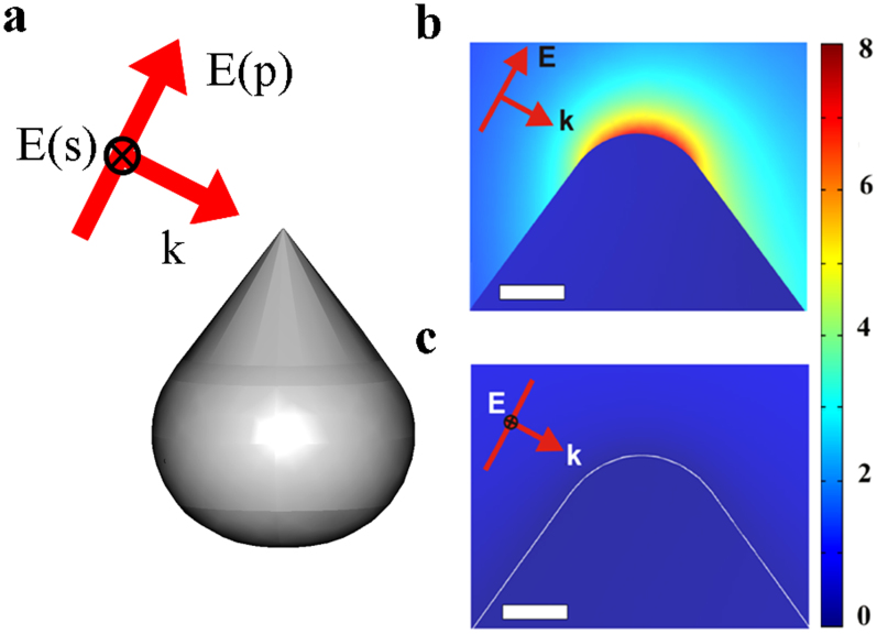
To analyze the observed array quantum efficiency and the polarization dependence of the laser-induced charge, we simulated the 3-dimensional optical electric field distribution at the tip using a finite-element electromagnetic field solver (COMSOL Multiphysics). We approximated the molybdenum emitter by a cone terminated by a 10 nm radius half sphere which represents the tip apex. To avoid parasitic interference at discontinuous surfaces, we truncated the emitter base and terminated it with a ~550 nm-radius spherical surface. In actual nanotip arrays with the gate electrodes, the diffraction and reflection at gate electrode edges and in the emitter cavity can cause interferences; here such effects are neglected. The assumed droplet-shaped emitter geometry is shown in Fig. 2 (a). Molybdenum and gold dielectric functions were taken from Ref. 13.
Figure 2. Calculated optical electric field distribution normalized to the incident field around the emitter tip for 800 nm-wavelength radiation and a 60° incident angle on a molybdenum emitter approximated by a droplet-shaped geometry shown in (a), for (b) p-polarized and (c) s-polarized cases.
Scale bars represent 10 nm.
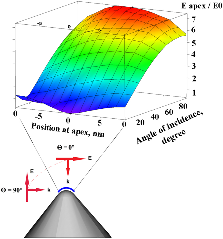
Optical electric field distributions of 800 nm-wavelength radiation with 60° incident angle are shown in Figs. 2 (b) and (c) in the case of p-polarized and s-polarized laser pulses, respectively. Local enhancement of the optical electric field of the p-polarized radiation at the tip apex, which is absent in the case of s-polarized radiation, is apparent. This is consistent with the experiment shown in Fig. 1 (c). Fig. 3 shows the dependence of the optical electric field distribution for p-polarized laser pulses as a function of the incident angle (the electric field values were taken at 0.5 nm above the tip surface). The optical electric field enhancement increases with the incident angle and saturates as the angle approaches 90°. Althouth the field enhancement is 20–30% higher at 90° than at 60°, it is difficult to reach 90° with the gated-FEAs because of the shadowing of the tips by the gate apertures.
Figure 3. Optical electric field distribution normalized to the incident field of 800 nn-wavelength radiation around the molybdenum emitter tip at different incident angles for the p-polarized case.
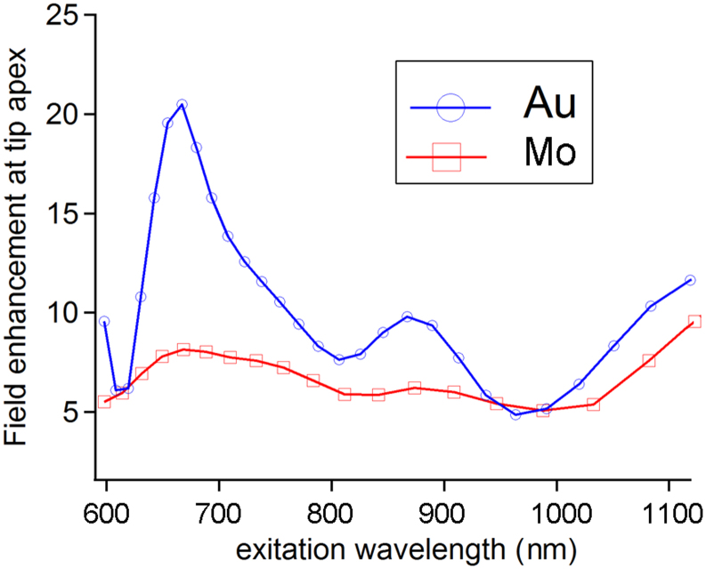
Much higher optical field enhancement is not expected at different wavelengths for the molybdenum emitter tips. As shown in Fig. 4, it depends only weakly on the excitation wavelength. This is in stark contrast to the case of a gold emitter tip. Although the field enhancement at ~800 nm is approximately the same for the two materials, the gold tip exhibits a ~3 higher field enhancement at ~680 nm via surface-plasmon resonance. We note however that, since the melting temperature of molybdenum (2625°C) is more than twice as high as that of gold (1063°C), molybdenum emitters are likely to sustain higher tip-current density and tip current than gold emitters.
Figure 4. The variation of the optical electric field enhancement with the excitation wavelength for molybdenum and gold emitters.
Enhanced light excitation in sub-micron-pitch nanotip array
Therefore, to further increase the bunch charge and the array quantum efficiency, we consider in the following increasing the emitter density by reducing the emitter array pitch. On one hand, the array quantum efficiency should increase proportionally to the array density. On the other hand, the smaller array pitch and the smaller gate aperture diameters will limit the laser excitation of the tip as the gate aperture diameters become small14. To surmount this problem, we propose a sub-micron pitch array with gold gate electrode and to take advantage of the extraordinary optical transmission (EOT)15 through sub-wavelength hole arrays at normal incidence.
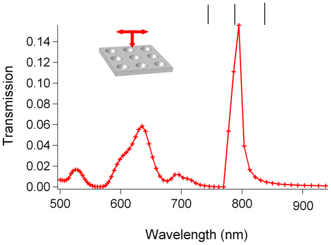
First, we consider the transmission through a 200 nm-thick free-standing gold film perforated by 250 nm-diameter holes arranged with a 750 nm-period. As shown in Figure 5, the transmission is resonantly enhanced around 790 nm by EOT15,16 for normal incidence; the light intensity is efficiently coupled to the gold film via the surface plasmon resonance, part of which is funneled into the aperture holes. The sub-wavelength diameter holes act as plasmonic waveguides with a TM-polarized transmission mode.
Figure 5. Transmission spectrum through a 200 nm-thick perforated gold film calculated for an array pitch of 750 nm and hole diameters equal to 250 nm (see inset).
To investigate whether the concept of EOT applied to FEAs can enhance the light excitation efficiency on the nanometer-sharp emitter array, we calculated the electromagnetic field distribution in an array of cone-shaped molybdenum nanotips with the period of 750 nm. The design of a single unit cell is depicted in Fig. 6. The 170 nm tall emitter tip is centered below the gate. The aperture diameter of the gold gate electrode is 250 nm and the molybdenum substrate and the gold gate electrode are separated by 300 nm. A monochromatic electromagnetic wave is incident from the top and normal to the gold surface. The calculation was done assuming periodic boundary conditions at the side surfaces and absorbing boundary conditions at the top and the bottom surface.
Figure 6. Single-cell gated FEA geometry with sub-micron pitch emitter array and gold gate electrode assumed in the electromagnetic simulation.
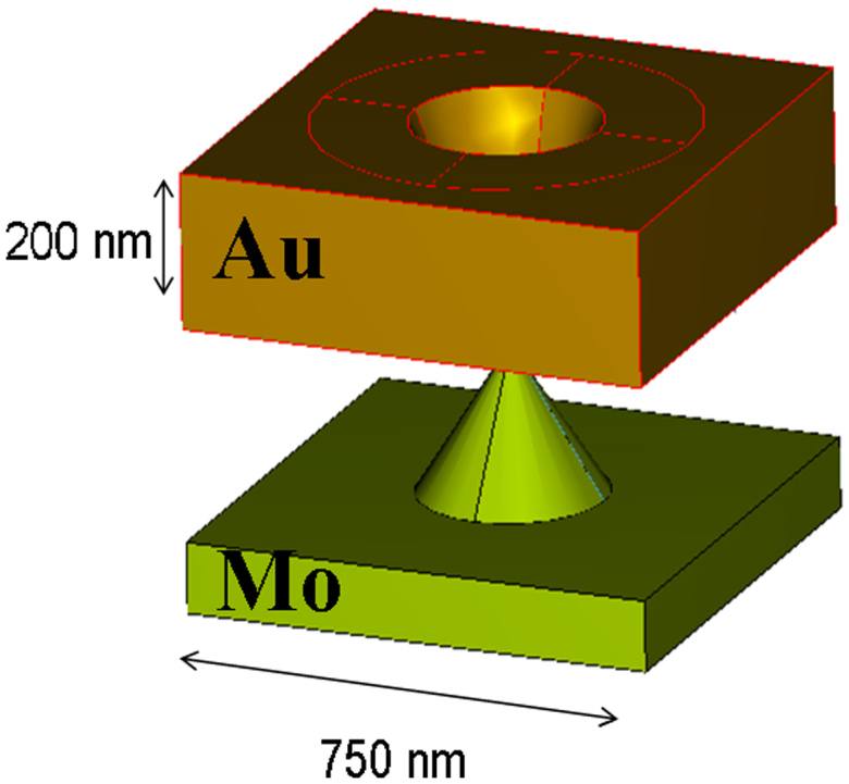
Figure 7 shows the x-z cross-section of the electromagnetic field distribution for a gold gate electrode, without (a, b, c) and with an emitter tip (d, e, f), calculated at a wavelength of 750 nm, 790 nm, and 842 nm. These three wavelengths are marked in Fig. 5 by vertical lines. The incident electric field is parallel to the x-axis. The calculations showed that the electromagnetic field in the cavity below the gold gate is resonantly enhanced at 790 nm, the same wavelength at which the EOT resonance occurs for the perforated gold film without emitter tips. Higher electric field beneath the gates is observed at 842 nm. However, because of the symmetry of the transmitted electromagnetic field and the tip geometry, the excitation intensity at the emitter tip apex is vanishingly small. This is related to the fact that diametrically opposed points on the tip surface have opposite charges of laser-induced surface charge density17.
Figure 7. Cross-sectional optical electric field distribution normalized to the incident field through apertures for (a,b,c) free-standing gold film, and (c,d,e) molybdenum nanotips with gold gate with the aperture holes same as (a–c), calculated for the radiation with the wavelength of 750 nm, 800 nm, and 842 nm.
Simulations with oblique angles of incidence at the resonance wavelength did not improve the situation; the field distribution in the hole remains almost symmetric. We therefore modified the single-cell geometry, in which the emitter tip is displaced in the x-direction by 50 nm from the center to one side while keeping the other parameters unchanged. Fig. 8 (a) shows the calculated cross-sectional electromagnetic field distribution at the wavelength of 842 nm in the x-z plane with the same electric field polarization as in Fig. 7. More than a factor of 4 enhancement of the optical electric field at the emitter tip apex is observed. Figs. 8 (b) and (c) show the close ups of the cross-sectional field distribution near the tip in the plane of the laser polarization (x-z plane) and in the plane perpendicular to it (y-z plane), respectively. From these calculations we deduce that the array quantum efficiency at a wavelength of 800 nm and normal incidence (Fig. 8) is a factor of ~30 higher compared to the value simulated for the 5 µm-pitch FEAs with an incident angle of 60°. When we compare it to the value obtained for normal incidence, the array quantum efficiency is even more than ~103 times higher. We expect a further increase of the array quantum efficiency by optimizing the gate electrode design, for example, introducing an asymmetry to the gate aperture shape and a sidewall slope at the gate aperture edge, which will induce evanescent fields predominantly at the bottom side of the gate in close proximity of the tip apexes18.
Figure 8.
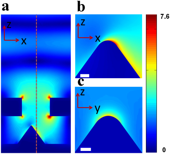
(a) Cross-sectional optical electric field distribution normalized to the incident field for the gated FEA single-cell with the displaced emitter tip, through the plane, which contains the electric field of the incident radiation and the emitter tip apex. (b) Same as (a) but in the perpendicular direction through the emitter tip. The scale bars show 10 nm.
Discussion
This work presents the first step towards the realization of optically driven submicron-pitch FEAs for the generation of high charge ultrafast electron pulses. A sub-micron-pitch FEA with a gold gate electrode that benefits from EOT is proposed and analyzed theoretically. It was found that the presence of the emitter tip apex does not alter the EOT resonance but the net excitation efficiency is low when the emitter tip is placed at the center of the aperture. We therefore considered a displaced emitter tip geometry and found a reasonably high field enhancement at the tip apex for normal incidence. From this, the estimated array quantum efficiency reaches a value in the order of 10−6. This is ~30 times larger than the case with 5 µm-pitch arrays excited at the laser incident angle of 60°. The possibility of normal incidence laser illumination of the high-density FEA structure studied in this work is beneficial in actual applications. For example, it eliminates the electron pulse broadening due to the pulse front tilt from a few ps (in the case of 60° incidence) down to ~100 fs (in the case of 2° tilt), although the bandwidth of the EOT resonance limits the shortest electron pulse duration to ~100 fs. We note that the array quantum efficiency is about a factor of 60 lower than quantum efficiency of flat photocathodes (6×10⁻⁵ for Copper19) exited by ultra-violet lasers. However, the use of nantip arrays eliminates the necessity to generate UV harmonics of the driving laser thereby simplifying the optical setup and increasing the overall efficiency by the reciprocal of the UV harmonic generation efficiency. Moreover, the field emitter arrays allow advaced beam collimation by integration on chip second gate electrode, which serves as an electrostatic lense20.
The proposed sub-micron-pitch nanotip array is also of particular interest for accelerator applications, which require the installation of the FEA into an electron gun with high acceleration electric fields5. As an example, to generate the baseline cathode performance specification of the SwissFEL X-ray free electron laser9 of 200 pC electron pulses with 10 ps duration, a sub-micron-pitch nanotip array with 1 mm-diameter requires the same amount of the laser pulse energy (~0.1 mJ) as the previous experiment (5 pC generation from the 5 µm-pitch array with 2 mm-diameter). Since this reduces the required tip current significantly, down to ~10−5 A, the associated space charge degradation on the pulse duration and the emittance are largely suppressed in the typical high acceleration electric field in the order of 108 V/m for the accelerator applications21. The fabrication of the proposed sub-micron-pitch nanotip arrays through the combination of molding and self-aligned gate processes, as well as by electron-beam lithography is under way.
Author Contributions
A.M., P.B. and S.T. conducted the laser induced field emission experiment and analyzed the experimental data. E.K. fabricated the FEA structure. T.F. and S.T. guided the project and participated in data analysis. A.M. performed the electromagnetic simulations. A.M., S.T. and T.F. wrote the paper.
Acknowledgments
This work is performed as a part of SwissFEL project at Paul Scherrer Institut and partially supported by the Swiss National Science Foundation 200021_125084.
References
- Crewe A. V. Scanning electron microscope: is high resolution possible? Science 154, 729–738 (1966). [DOI] [PubMed] [Google Scholar]
- Spence J. C. H. Experimental High Resolution Electron Microscopy (Oxford University Press, 2009). [Google Scholar]
- Schwoebel P. R. Field emission arrays for medical x-ray imaging. Appl. Phys. Lett. 88, 113902 (2006). [Google Scholar]
- Whaley D. R. Experimental demonstration of an emission-gated traveling-wave tube amplifier. IEEE Trans. Plasma Science 30, 998–1008 (2002). [Google Scholar]
- Tsujino S., Paraliev M., Kirk E., Gough C., Ivkovic S. & Braun H. H. Sub-nanosecond switching and acceleration to relativistic energies of field emission electron bunches from metallic nano-tips. Phys. Plasmas 18, 064502 (2011). [Google Scholar]
- Hommelhoff P., Sortais Y., Aghjani-Talesh A. & Kasevich M. A. Field emission tip as a nanometer source of free electron femtosecond pulses. Phys. Rev. Lett. 96, 077401 (2006). [DOI] [PubMed] [Google Scholar]
- Ropers C., Scolli D. R., Schulz C. P., Lienau C. & Elsaesser T. Localized multiphoton emission of femtosecond electron pulses from metal nanotips. Phys. Rev. Lett. 98, 043907 (2007). [DOI] [PubMed] [Google Scholar]
- Yanagisawa H., Hafner C., Dona P., Klockner M., Leuenberger D., Greber T., Hengsberger M. & Osterwalder J. Optical control of field-emission sites by femtosecond laser pulses. Phys. Rev. Lett. 103, 257603 (2009). [DOI] [PubMed] [Google Scholar]
- Patterson B. et al. Coherent science at the SwissFEL x-ray laser. New J. Physics 12, 035012 (2010). [Google Scholar]
- Graves W. S., Kärtner F. X., Moncton D. E. & Piot P. Intense superradiant x rays from a compact source using a nanocathode array and emittance exchange. Phys. Rev. Lett. 108, 263904 (2012). [DOI] [PubMed] [Google Scholar]
- Tsujino S., Beaud P., Kirk E., Vogel T., Sehr H., Gobrecht J. & Wrulich A. Ultrafast electron emission from metallic nanotip arrays induced by near infrared femtosecond laser pulses. Appl. Phys. Lett. 92, 193501 (2008). [Google Scholar]
- Mustonen A., Beaud P., Kirk E., Feuer T. & Tsujino S. Five picocoulomb electron bunch generation by ultrafast laser-induced field emission from metallic nano-tip arrays. Appl. Phys. Lett. 99, 103504 (2011). [Google Scholar]
- Palik E. D., ed. Handbook of Optical Constants of Solids (Academic, 1998). [Google Scholar]
- Bethe H. A. Theory of diffraction by small holes. Phys. Rev. 66, 163–182 (1944). [Google Scholar]
- Ebbesen T. W., Lezec H. J., Ghaemi H. F., Thio T. & Wolff P. A. Extraordinary optical transmission through sub-wavelength hole arrays. Nature 391, 667–669 (1998). [Google Scholar]
- Lezec H. J. & Thio T. Diffracted evanescent wave model for enhanced and suppressed optical transmission through subwavelength hole arrays. Optics Express 12, 3629–3651 (2004). [DOI] [PubMed] [Google Scholar]
- Novotny L. Theory of Nanometric Optical Tweezers. Phys. Rev. Lett. 79, 4 (1997). [Google Scholar]
- Beermann J., Søndergaard T., Novikov S. M., Bozhevolnyi S. I., Devaux E. & Ebbesen Thomas W. Field enhancement and extraordinary optical transmission by tapered periodic slits in gold films. New J. Phys. 13, 063029 (2011). [Google Scholar]
- Ding Y. et al. Measurements and simulations of ultralow emittance and ultrashort electron beams in the linac coherent light source. Phys. Rev. Lett. 102, 254801 (2009). [DOI] [PubMed] [Google Scholar]
- Helfenstein P. et al. Highly collimated electron beams from double-gate field emitter arrays with large collimation gate apertures. Appl. Phys. Lett. 98, 061502 (2011). [Google Scholar]
- Dehler M. Design and modeling of field emitter arrays for a high brilliance electron source. Proc. 9th ICAP, 114–117 (2006). [Google Scholar]


