Abstract
A heterojunction photodiode was fabricated from ZnO nanowires (NWs) grown on a p-type Si (100) substrate using a hydrothermal method. Post growth hydrogen treatment was used to improve the conductivity of the ZnO NWs. The heterojunction photodiode showed diode characteristics with low reverse saturation current (5.58 × 10⁻⁷ A), relatively fast transient response, and high responsivity (22 A/W at 363 nm). Experiments show that the photoresponsivity of the photodiode is dependent on the polarity of the voltages. The photoresponsivity of the device was discussed in terms of the band diagrams of the heterojunction and the carrier diffusion process.
Semiconductor nanowires (NWs) have garnered extensive research interests due to their unique optical and electrical properties.1, 2 In particular, ZnO NWs are promising for optoelectronic applications including ultraviolet (UV) light-emitting diodes (LED), UV laser diodes, and UV photodetectors for their wide band gap (3.37 eV), large exciton binding energy 60 meV, and high photoconductive gain.3, 4, 5 The development of a ZnO pn junction has been limited by the difficulty of growing p-type ZnO. However, heterojunctions with ZnO NWs have been developed with p-type substrates including silicon.6, 7, 8, 9 The traditional bottom up approach is often employed which causes poor conductivity and high density of surface defects. Post growth hydrogen treatment is a simple and efficient method for the conductivity enhancement, which is intensively investigated both theoretically and experimentally.10, 11, 12, 13, 14 The conductivity of ZnO could be enhanced by up to three orders of magnitude without significant changes in the structure and crystal orientation of the wurtzite type ZnO nanostructures.12 The conductivity enhancement could be attributed to the introduction of shallow donor states such as the VO-H complex and the hydrogen interstitial.15, 16 Also, the passivation effect on the defects could reduce carrier scattering centers and hence has the potential to increase the electron mobility.17
In this study, heterojunction photodiode was fabricated based on highly vertically aligned hydrogen treated ZnO NWs grown on top of p-Si substrate through hydrothermal method. A similar growth method has been reported by Ghosh and Basak for quasialigned ZnO NWs/p-Si heterojunction photodiode.8 The heterojunction photodiode in this work shows a low reverse saturation current and relatively fast time response. The photoresponsivity spectra of the device in the UV and visible regions depend on the polarity of the applied voltages, which is explained in terms of energy band structure and carriers transportation mechanism inside the heterojunction structure.
All chemical reagents were purchased from Sigma-Aldrich and used without further purification. Ammonium hydroxide (28 wt. %) was added dropwise into 0.1M zinc chloride solution until the pH is 10-11 and the solution was clear. Subsequently, the transparent solution was transferred to a Teflon-lined autoclave (Parr, USA) and the silicon substrate with ZnO nanoparticles (NPs) as a seed layer was suspended in the solution at 95 °C for 3 h in a regular laboratory oven. Then, the growth solution was cooled down to room temperature naturally. The resulting substrate was thoroughly washed with deionized water and absolute ethanol for several times and dried in air at room temperature followed by post-annealing treatment in Ar/H2 (ratio, 96:4) atmosphere at 400 °C for 2 h. In order to form good metal contact on top of the ZnO NWs, a thin layer of the polyvinyl-alcohol (PVA) coated ZnO NPs was spin coated on top of the ZnO NWs to cover the space between ZnO NWs. Detailed discussion about the optical properties of the PVA coated ZnO nanoparticles (PVA-ZnO NPs) can be found in our previous work.18 Finally, 250 nm aluminum was deposited on top of ZnO NWs and p-Si through a shadow mask by E-beam evaporator to form the contacts of the photodiode.
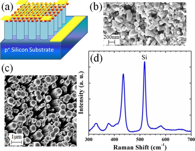
Figure 1a illustrates the three dimensional view of the structure of the photodiode. Top contacts with interdigitated patterns were used to enhance the carrier collection efficiency. The morphologies of the PVA-ZnO NPs and the hydrogen treated ZnO NWs are shown in Figures 1b, 1c, respectively. Note that the average diameter of the PVA-ZnO NPs and for ZnO NWs is about 150 nm and 250 nm, respectively. The length of the ZnO NWs can be easily controlled by varying the reaction time. The Raman spectra presented in Figure 1d proves the high quality of the hydrogen treated ZnO NWs.19
Figure 1.
(a) 3D view of heterojunction photodiode fabricated from ZnO NWs grown on top of p-Si substrates. (b) A SEM image showing the morphology of the PVA coated ZnO nanoparticles on top of the ZnO NWs and (c) hydrogen treated ZnO NWs on top of p-Si substrates. (d) Raman spectra of the hydrogen treated ZnO NWs on top of p-Si substrate.
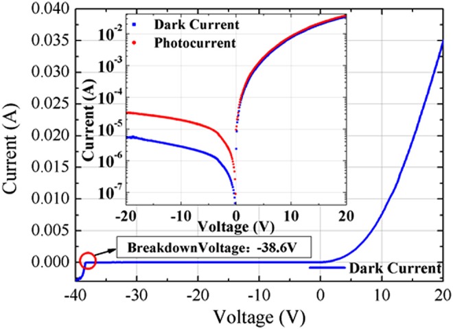
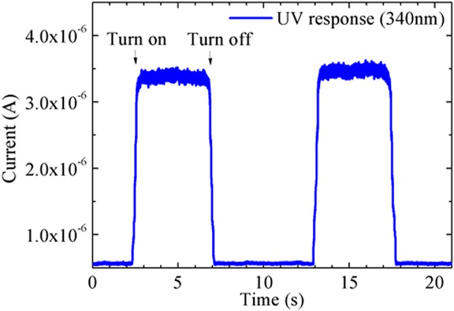
The I-V characteristic of the fabricated heterojunction photodiode is shown in Figure 2, which was measured under dark environment. The ideality factor n was determined to be 12.36 by fitting the measured I-V curve. The breakdown was observed at −38.6 V, higher than all published results for n-ZnO/p-Si heterojunctions.20, 21, 22, 23, 24 The reverse saturation current is 5.58 × 10⁻⁷ A, which is between the reported values 2 × 10⁻⁵ A and 0.17 × 10⁻⁹ A.7, 8 Under forward bias voltages, the dark current increases exponentially following the equation, I ∼ exp(αV), which is usually observed in the wide band gap p-n diodes due to a recombination-tunneling mechanism.8, 25 The constant α was evaluated to be 2.5 V−1 by fitting the experimental data as shown in Figure 2. The inset of Figure 2 presents both the dark current and photocurrent measured with UV illumination (340 nm). Under forward bias conditions, no significant changes in the current occurred upon illumination with UV light. In contrast, the photocurrent to dark current ratio is about 6–7 under reverse bias conditions. The transient response of the ZnO NWs/p-Si heterojunction photodiode is shown in Figure 3, which was measured by turning on and off a 340 nm UV LED. The rising time (as measured from 10% to 90%) and falling time (from 90% to 10%) of the device were measured to be 0.29 and 0.34 s, respectively. The relatively fast time response is likely due to the conductivity improvement and the surface passivation of the ZnO NWs by hydrogen treating.
Figure 2.

I-V curve of the photodiode measured under dark environment. Inset: I-V curve measured under dark and under UV illumination.
Figure 3.

Time response of the ZnO NWs/p-Si heterojunction photodiode with a 0.29 s rising time and 0.34 s falling time measured under ambient conditions.
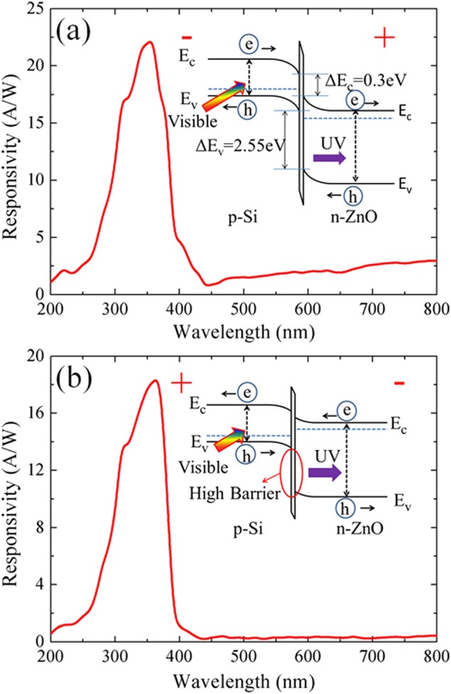
The photoresponsivity spectra of the ZnO NWs/p-Si heterojunction photodiode under reverse and under forward bias conditions are shown in Figures 4a, 4b, respectively. A maximum responsivity of 22 A/W for UV light (363 nm) at 20 V reverse bias was observed. According to the best of our knowledge, this responsivity is at least 30 times higher than most of the published results.6, 26, 27, 28, 29 However, this is lower than the responsivity of n-ZnO/p-Si heterojunction photodiode fabricated using DC magnetron sputtering method reported by Kosyachenko et al., which can reach to 210 A/W at 390 nm with −5 V bias.30 Under reverse bias conditions, a monotonous increase of the photoresponsivity with increasing wavelength was observed in the visible range (450–800 nm). In contrast, the responsivity in the visible region when forward biased was relatively low and remains nearly unchanged with increasing wavelength. It is also found that the UV responsivity under the forward biased condition is slightly lower than that under reverse bias conditions. These photoresponse results can be understood by referring to the energy band diagram and a carrier transport mechanism of the heterojunction structures under in the insets of Figures 4a, 4b, respectively.
Figure 4.

Photoresponsivity spectra of the ZnO NWs/p-Si heterojunction photodiode measured under (a) reverse and (b) forward biases. Inset: energy band diagrams and carrier transportation mechanisms.
The optical bandgap of the ZnO NWs is dependent on the growth temperature of the hydrothermal process, which can vary from 3.28 eV to 3.41 eV.31, 32, 33 In this work, the bandgap of the ZnO NWs is determined to be 3.37 eV from the absorption measurement (not shown here). Based on the Anderson's model,34 the heterojunction has a small conduction band offset 0.3 eV and a large valance band offset 2.55 eV. Since ZnO is highly transparent to light in the visible region, most of the visible light will be absorbed in the p-Si substrate and generate electron-hole pairs (EHP). Under reversed bias conditions, these photogenerated electrons will pass through the interfacial barriers easily and drift toward the ZnO NWs region driven by the external electrical field. At the same time, the photogenerated holes will drift toward the contacts in the p-Si side and be collected to form the photocurrent signal. To the contrary, when the heterojunction is forward biased, the photogenerated holes in the p-Si side will drift toward the ZnO NWs region but they cannot get over the high potential barriers in the interfacial region. Thus, the visible photoresponsivity under forward bias conditions is mainly due to the transportation of photogenerated electrons (minority carriers) in p-Si, which is very low in magnitude.
For the slightly lower UV photoresponsivity observed under forward bias condition, the mechanism is similar as that of in the visible region. Due to the limited penetration depth of UV light (36–40 nm) in ZnO, most of the UV light is absorbed by ZnO NWs.27 When reverse biased, the UV generated EPH can easily move across the interfacial region and be collected by the contacts. However, under forward bias conditions, the UV generated electrons in the ZnO NWs region will move toward the p-Si side and therefore need to pass through a small potential barrier in the interfacial region. Since this barrier is small (0.3 eV), most of the UV generated electrons can get over this barrier and finally be collected by the contacts in the p-Si side.
In conclusion, ZnO NWs/p-Si heterojunction photodiode was fabricated using a simple hydrothermal method followed by post growth hydrogen treatment. The heterojunction photodiode shows low reverse saturation current, relatively fast transient response, and high responsivity. The photoresponsivity spectra of the device in the UV and visible regions are dependent on the polarity of the applied voltages, which is due to the large valance band offset and carrier transportation mechanism inside the heterojunction structure.
Acknowledgments
The authors gratefully acknowledge support from National Security Technologies through NSF Industry/University Cooperative Research Center Connection One. The authors also acknowledge the National Science Foundation Smart Lighting Engineering Research Center (EEC-0812056) and a NSF career award DMR 1151028. The author Mingpeng Yu thanks for the financial support from China Scholarship Council (CSC File No.2010646040).
References
- Garnett E. and Yang P., Nano Lett. 10, 1082 (2010). 10.1021/nl100161z [DOI] [PubMed] [Google Scholar]
- Soci C., Zhang A., Xiang B., Dayeh S. A., Aplin D. P. R., Park J., Bao X. Y., Lo Y. H., and Wang D., Nano Lett. 7, 1003 (2007). 10.1021/nl070111x [DOI] [PubMed] [Google Scholar]
- Lai E., Kim W., and Yang P., Nano Res. 1, 123 (2008). 10.1007/s12274-008-8017-4 [DOI] [Google Scholar]
- Chu S., Wang G., Zhou W., Lin Y., Chernyak L., Zhao J., Kong J., Li L., Ren J., and Liu J., Nat. Nanotechnol. 6, 506 (2011). 10.1038/nnano.2011.97 [DOI] [PubMed] [Google Scholar]
- Das S. N., Moon K.-J., Kar J. P., Choi J.-H., Xiong J., Lee T. I., and Myoung J.-M., Appl. Phys. Lett. 97, 022103 (2010) 10.1063/1.3464287 [DOI] [Google Scholar]
- Luo L., Zhang Y., Mao S. S., and Lin L., Sens. Actuators, A 127, 201 (2006). 10.1016/j.sna.2005.06.023 [DOI] [Google Scholar]
- Ye J. D., Gu S. L., Zhu S. M., Liu W., Liu S. M., Zhang R., Shi Y., and Zheng Y. D., Appl. Phys. Lett. 88, 182112 (2006). 10.1063/1.2201895 [DOI] [Google Scholar]
- Ghosh R. and Basak D., Appl. Phys. Lett. 90, 243106 (2007). 10.1063/1.2748333 [DOI] [Google Scholar]
- Al-Heniti S. H., J. Nanosci. Nanotechnol. 10, 6606 (2010). 10.1166/jnn.2010.2545 [DOI] [PubMed] [Google Scholar]
- Ohyama M., Kozuka H., and Yoko T., J. Am. Ceram. Soc. 81, 1622 (1998). 10.1111/j.1151-2916.1998.tb02524.x [DOI] [Google Scholar]
- Van de Walle C. G., Phys. Rev. Lett. 85, 1012 (2000). 10.1103/PhysRevLett.85.1012 [DOI] [PubMed] [Google Scholar]
- Hsu C.-H. and Chen D.-H., Nanotechnology 21, 285603 (2010). 10.1088/0957-4484/21/28/285603 [DOI] [PubMed] [Google Scholar]
- Dev A., Niepelt R., Richters J. P., Ronning C., and Voss T., Nanotechnology 21, 065709 (2010). 10.1088/0957-4484/21/6/065709 [DOI] [PubMed] [Google Scholar]
- Ohashi N., Ishigaki T., Okada N., Sekiguchi T., Sakaguchi I., and Haneda H., Appl. Phys. Lett. 80, 2869 (2002). 10.1063/1.1470703 [DOI] [Google Scholar]
- Janotti A. and Van de Walle C. G., Nature Mater. 6, 44 (2007). 10.1038/nmat1795 [DOI] [PubMed] [Google Scholar]
- Cai P. F., You J. B., Zhang X. W., Dong J. J., Yang X. L., Yin Z. G., and Chen N. F., J. Appl. Phys. 105, 083713 (2009). 10.1063/1.3108543 [DOI] [Google Scholar]
- Varley J. B., Peelaers H., Janotti A., and Van de Walle C. G., J. Phys.: Condens. Matter 23, 334212 (2011). 10.1088/0953-8984/23/33/334212 [DOI] [PubMed] [Google Scholar]
- Qin L., Shing C., Sawyer S., and Dutta P. S., Opt. Mater. 33, 359 (2011). 10.1016/j.optmat.2010.09.020 [DOI] [Google Scholar]
- Li C., Hong G., Wang P., Yu D., and Qi L., Chem. Mater. 21, 891 (2009). 10.1021/cm802839u [DOI] [Google Scholar]
- Reddy N. K., Ahsanulhaq Q., Kim J. H., and Hahn Y. B., Appl. Phys. Lett. 92, 043127 (2008). 10.1063/1.2839579 [DOI] [Google Scholar]
- Ismail R. A., Al-Naimi A., and Al-Ani A. A., Semicond. Sci. Technol. 23, 075030 (2008). 10.1088/0268-1242/23/7/075030 [DOI] [Google Scholar]
- Zhang Y., Xu J., Lin B., Fu Z., Zhong S., Liu C., and Zhang Z., Appl. Surf. Sci. 252, 3449 (2006). 10.1016/j.apsusc.2005.04.053 [DOI] [Google Scholar]
- Li X., Zhang B., Zhu H., Dong X., Xia X., Cui Y., Ma Y., and Du G., J. Phys. D: Appl. Phys. 41, 035101 (2008). 10.1088/0022-3727/41/3/035101 [DOI] [Google Scholar]
- Al-Heniti S., Badran R. I., Al-Ghamedi A. A., and Al-Agel F. A., Adv. Sci. Lett. 4(1), 24 (2011). 10.1166/asl.2011.1196 [DOI] [Google Scholar]
- Fedison J. B., Chow T. P., Lu H., and Bhat I. B., Appl. Phys. Lett. 72, 2841 (1998). 10.1063/1.121475 [DOI] [Google Scholar]
- Um H.-D., Moiz S. A., Park K.-T., Jung J.-Y., Jee S.-W., Ahn C. H., Kim D. C., Cho H. K., Kim D.-W., and Lee J.-H., Appl. Phys. Lett. 98, 033102 (2011). 10.1063/1.3543845 [DOI] [Google Scholar]
- Jeong I.-S., Kim J. H., and Lm S., Appl. Phys. Lett. 83, 2946 (2003). 10.1063/1.1616663 [DOI] [Google Scholar]
- Gupta B., Jain A., and Mehra R. M., J. Mater. Sci. Technol. 26, 223 (2010). [Google Scholar]
- Park C. H., Jeong I. S., Kim J. H., and Im S., Appl. Phys. Lett. 82, 3973 (2003). 10.1063/1.1579553 [DOI] [Google Scholar]
- Kosyachenko L. A., Lashkarev G. V., Sklyarchuk V. M., Levtushenko A. I., Sklyarchuk O. F., Lazorenko V. I., and Ulyashin A., Phys. Status Solidi A 10, 1002 (2010). [Google Scholar]
- Ni Y.-h., Wei X.-w., Hong J.-m. and Ye Y., Mater. Sci. Eng., B 121, 42–47 (2005). 10.1016/j.mseb.2005.02.065 [DOI] [Google Scholar]
- Unalan H. E., Hiralal P., Rupesinghe N., Dalal S., Milne W. I., and A J Amaratunga G., Nanotechnology 19, 255608 (2008). 10.1088/0957-4484/19/25/255608 [DOI] [PubMed] [Google Scholar]
- Akgun M. C., Kalay Y. E., and Unalan H. E., J. Mater. Res. 27, 1445 (2012). 10.1557/jmr.2012.92 [DOI] [Google Scholar]
- Sze S. M., Physics of Semiconductor Devices, 2nd ed. (Wiley, New York, 1981). [Google Scholar]


