Abstract
Fabrication of thin-film solar cells (TFSCs) on substrates other than Si and glass has been challenging because these nonconventional substrates are not suitable for the current TFSC fabrication processes due to poor surface flatness and low tolerance to high temperature and chemical processing. Here, we report a new peel-and-stick process that circumvents these fabrication challenges by peeling off the fully fabricated TFSCs from the original Si wafer and attaching TFSCs to virtually any substrates regardless of materials, flatness and rigidness. With the peel-and-stick process, we integrated hydrogenated amorphous silicon (a-Si:H) TFSCs on paper, plastics, cell phone and building windows while maintaining the original 7.5% efficiency. The new peel-and-stick process enables further reduction of the cost and weight for TFSCs and endows TFSCs with flexibility and attachability for broader application areas. We believe that the peel-and-stick process can be applied to thin film electronics as well.
Thin-film solar cells (TFSCs), such as hydrogenated amorphous silicon (a-Si:H), cadmium telluride (CdTe) and copper indium gallium selenide (CIGS), are dominantly fabricated on Si wafer or glass substrates1,2,3. Recently, TFSCs are also fabricated on cheaper, lighter or flexible substrates, such as metal foils4 and polyimide5,6 substrates. However, the fabrication processes or material deposition conditions for TFSCs typically need to be modified to accommodate the temperature limitation and flatness of these substrates, which can adversely affect the efficiency and fabrication yield of TFSCs6,7,8. Furthermore, even with the modified fabrication conditions, TFSCs cannot be fabricated on even cheaper, lighter, and more flexible substrates, such as paper, textile and rubber, because these nonconventional substrates easily deform at as low temperature as around 120°C and are not flat and rigid enough for handling9,10. Fabricating TFSCs on these substrates will significantly broaden their application areas, such as portable power supplies11, wearable electronics12 and aerospace applications13. Therefore, there is a great need for developing new methods to fabricate TFSCs on universal substrates, without modifying existing fabrication conditions and adversely affecting the efficiency.
Results
Herein, we report a novel peel-and-stick process to fabricate efficient TFSCs onto virtually any substrates regardless of materials, roughness and rigidness without changing the material deposition conditions and performance of TFSCs. The peel-and-stick process includes two steps: 1) peeling-off fully fabricated TFSCs in water from the nickel (Ni) coated Si wafer used for fabrication, and 2) attaching the peeled-off TFSCs to the surface of any substrate. The peeling process relies on the phenomenon of water-assisted subcritical debonding at interface between Ni and silicon dioxide (SiO2), which separates the metallic layer together with TFSCs from the original Si wafer14,15. Since the peel-and-stick process does not require any fabrication on the final target substrate, it circumvents all the fabrication challenges associated with these nonconventional substrates discussed above. Importantly, the efficiency of the transferred TFSCs on any target substrate remains the same as the as-fabricated TFSCs on Si wafers. The procedures of the peel-and-stick process are illustrated in Figure 1. First, a Si/SiO2 wafer is coated with a Ni film (300 nm) by electron-beam (e-beam) evaporation, and subsequently TFSCs are deposited on top of the metallic layer using regular TFSC fabrication procedures (Figure 1a). Second, a thermal release tape (NittoDenko®) is attached to the top of the TFSCs serving as a temporary transfer holder. A transparent protection layer (ProTek®) is spin-casted in between the TFSCs and the thermal release tape to prevent the TFSCs from the tape polymer contamination and direct contact with water. Third, the entire structure is soaked in a water bath at room temperature. Inside the water bath, an edge of the thermal release tape is slightly peeled back to promote water penetration into the Ni and SiO2 interface. The Ni and SiO2 interface is separated due to the water-assisted subcritical debonding14,15, leading to the peeling-off the TFSCs from the original Si/SiO2 wafer (Figure 1b). Finally, the thermal release tape holding the peeled-off TFSCs is heated at 90°C for a few seconds to weaken its adhesion to the TFSCs. The TFSCs are then attached to various surfaces using common adhesive agents, such as double sided tapes or Polydimethylsiloxane (PDMS) (Figure 1c). After removing the thermal release tape, only the TFSCs are left on the target substrate, such as cell phone, paper, metal foils, plastics and textile (Figure 1d).
Figure 1. Procedures of the peel-and-stick process.
(a) As-fabricated TFSCs on the original Si/SiO2 wafer. (b) The TFSCs are peeled off from the Si/SiO2 wafer in a water bath at room temperature. (c) The peeled off TFSCs are attached to a target substrate with adhesive agents. (d) The temporary transfer holder is removed, and only the TFSCs are left on the target substrate.
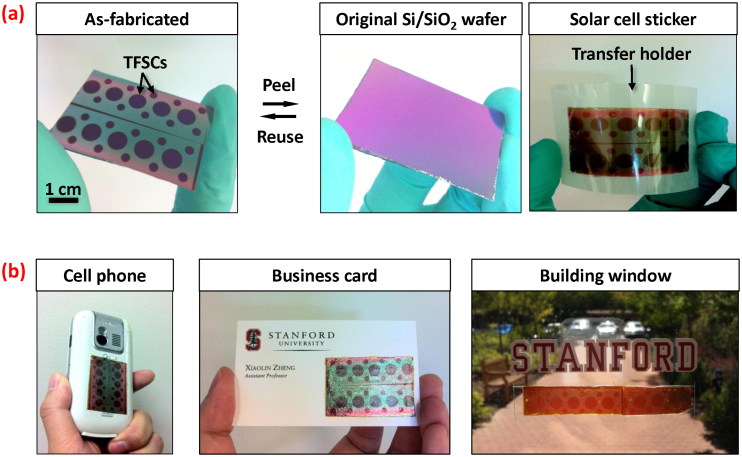
To demonstrate the peel-and-stick process, we use the a-Si:H TFSCs as our model system. The fabrication conditions for the a-Si:H TFSCs are identical to those that would have been usually used for fabricating TFSCs on Si wafers (See the method section for the TFSC fabrication details). Figure 2a (left image) shows a representative optical image of the as-fabricated a-Si:H TFSCs on the Ni coated Si/SiO2 wafer before the peel-and-stick process, as also described in figure 1a. The big and small round circles correspond to solar cells with an area of 0.28 cm2 or 0.05 cm2, respectively. After peeling-off the TFSCs in a water bath (Figure 1b), the Si wafer is clean and reusable (Figure 2a, middle image), and the TFSCs are held temporarily by the thermal release tape (Figure 2a, right image). Notably, the TFSCs after the peel-and-stick process show no visible damages. Next, the peeled-off TFSCs are attached to virtually any objects, including cell phone, business card, and building window (Figure 2b), and these objects are previously inaccessible due to the incompatibility issues with the existing TFSC fabrication facilities. The peel-and-stick process provides a simple way for integrating TFSCs into buildings, clothes, and many other nonconventional substrates.
Figure 2. TFSCs at different stages of the peel-and-stick process.
(a) As-fabricated TFSCs on the original Ni coated Si/SiO2 wafer (left). The donor Si/SiO2 wafer is clean and reusable after the peeling-off step (middle). The TFSCs are held by a temporary transfer holder (right). (b) TFSCs on cell phone (left), business card (middle), and building window (right).
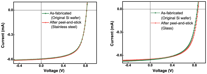
Importantly, the a-Si:H TFSCs show nearly identical efficiency before and after the peel-and-stick process. Figure 3 shows the current-voltage (I–V) characteristics of representative TFSCs before and after the peel-and-stick process to a sheet of stainless steel (left) or a soda-lime glass slide (right), and the I–V characteristics are indistinguishable, implying that no damages are induced in the TFSCs during the peel-and-stick process. Table 1 summarizes the average performance metrics over 20 solar cells with area of 0.05 cm2 and 0.28 cm2 respectively, showing η = 7.4 ± 0.5% and 5.2 ± 0.1% before the peel-and-stick process, and η = 7.6 ± 0.5% and η = 5.3 ± 0.1% after the peel-and-stick process. The efficiency difference in different sizes of solar cells is caused by large series resistance in larger solar cells16. Nevertheless, more important thing is that both solar cells have nearly identical efficiencies before and after the peel-and-stick process with only 5% variation that is within measurement errors. These results illustrate several key advantages of the present peel-and-stick process: versatility in substrate choices, high fidelity to original TFSC performance, simplicity and scalability of the procedures, and additional cost-saving features with reusable original Si/SiO2 wafers.
Figure 3. Comparisons of the TFSC performances before and after the peel-and-stick process.
The representative I–V characteristics (below average performance) of the as-fabricated TFSCs (green lines with stars) are the same as those after transferring the TFSCs (red lines with dots) to stainless steel (left) and soda-lime glass (right).
Table 1. Statistic summary of the average performance metrics over 20 a-Si:H TFSCs before and after the peel-and-stick process with only 5% variation that is within the measurement errors.
| As-fabricated (Original Si wafer) | After peel-and-stick (Glass) | |||
|---|---|---|---|---|
| Solar cell area (cm2) | 0.05 | 0.28 | 0.05 | 0.28 |
| JSC (mA/cm2) | 13.9 ± 1.0 | 10.8 ± 0.3 | 14.1 ± 1.0 | 11.0 ± 0.3 |
| VOC (V) | 0.848 ± 0.005 | 0.848 ± 0.005 | 0.851 ± 0.005 | 0.850 ± 0.005 |
| FF (%) | 62.8 ± 2.4 | 56.5 ± 0.9 | 63.6 ± 2.3 | 56.6 ± 1.9 |
| η (%) | 7.4 ± 0.5 | 5.2 ± 0.1 | 7.6 ± 0.5 | 5.3 ± 0.1 |
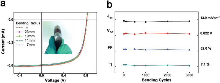
The applications of TFSCs may require intentional bending or non-planar shaping17,18. The peel-and-stick process also enables TFSCs to be integrated with flexible or curved surfaces (e.g., wavy building roof, helmets, and portable electronics). To demonstrate this, a-Si:H TFSCs are transferred on a flexible sheet of stainless foil (~0.2 mm thick) and manually bended as shown in figure 4a (inset). As a result, I-V characteristics of the TFSCs remain the same after bending the flexible sheet with a range of bending radius from ∞ down to 7 mm (Figure 4a). In addition, the solar cell performances are unchanged over 3000 cycles of bending with bending radius about 10 mm (Figure 4b), demonstrating the mechanical flexibility and robustness of the transferred TFSCs. It should be noted that the mechanical properties of the final solar cells are not determined by the peel-and-stick process, but rather by the intrinsic material properties and dimensions of the TFSCs (e.g., a-Si:H as an active material, indium tin oxide (ITO) as an electrode).
Figure 4. Mechanical flexibility of the transferred TFSCs.
(a) The I–V characteristics of the TFSCs remain the same after bending the flexible sheet with a range of bending radius from ∞ down to 7 mm. (b) The flexible TFSCs show no performance change over 3000 cycles of bending with bending radius about 10 mm. Note that all the I–V characteristics are measured when the TFSCs are flat to prevent any damage from the sharp tungsten probe tips during the measurements.
Discussion
In conclusion, we report a novel and versatile peel-and-stick process to directly build TFSCs on diverse previously inaccessible substrates, such as paper, plastic, cell phones, and buildings. The peel-and-stick process, while preserving the TFSC performance, circumvents the fabrication challenges associated with the nonconventional substrates by separating the fabrication process with the final target substrate. These previously inaccessible substrates for TFSCs enable further reduction of the cost and weight, and endow TFSCs with flexibility and attachability to greatly broaden their application areas. Though we only demonstrate the transfer of a-Si:H TFSCs herein, we believe that the peel-and-stick process can be applied to other kinds of TFSCs19 and thin film electronics20,21 as well.
Methods
Fabrication of the a-Si:H TFSCs
A Si wafer (500 μm thick) with thermally grown SiO2 (300 nm) was cleaned by the standard wafer cleaning procedures. The metallic layer (Ni, 300 nm) and subsequent Ag bottom electrodes (~1 μm) were deposited on the Si/SiO2 wafer at room temperature by using e-beam evaporation with deposition rate of around 1~3Å/sec. The a-Si:H TFSCs with n-i-p structure were deposited by plasma enhanced chemical vapor deposition (PECVD) in a multi-chamber cluster tool (MVSystems, Inc.) at a substrate temperature of approximately 200°C with 13.56 MHz RF power. The n-layer (20 nm) was grown using SiH4 and PH3/H2 with ETauc = 1.75 eV and σdark ~ 2×10⁻² S/cm. The i-layer (300 nm) was grown using SiH4 without hydrogen dilution with ETauc = 1.78 eV and σdark ~ 2×10⁻¹⁰ S/cm. The p-layer (8 nm) was grown using SiH4, BF3, and H2 with ETauc = 2.1 eV and σdark ~ 5×10⁻⁴ S/cm. Finally, ITO (90% In2O3, 10% SnO2) dots were RF sputtered at 200°C using an Ar/O2 mixture to define individual solar cells with the RF power of ~0.25 W/cm2 and deposition rate of ~1Å/sec.
Peel-and-stick process
The as-fabricated a-Si:H TFSCs were cleaned by solvents and dried on a hot plate at 120°C for 3 minutes. A transparent protection layer (ProTek®) was spin-casted at 3000 rpm and annealed at 110°C and 175°C for 3 minutes sequentially. The ProTek® residues at the Si wafer sidewalls were removed by a razor blade. After applying thermal release tape on top of the ProTek®, the whole structure was immersed into a water bath at room temperature. An edge of the thermal release tape was slightly peeled-off to initiate the water penetration, causing the separation of the Ni layer together with the TFSCs from the Si/SiO2 wafer. The lifted TFSCs were dried by N2 gun and heated at 90°C for around 30 seconds to weaken the adhesion of the thermal release tape. In the mean time, the target substrate was pasted or coated with commercial adhesive agents such as double sided tape or PDMS. Finally, the TFSCs were attached on the target substrate and the thermal release tape was removed. The ProTek® protection layer was then removed by remover for the I–V curve measurements.
Characterization of the TFSCs
The solar cell properties were characterized under AM 1.5G illumination (Class AAA solar simulator, Model 94063A, Oriel). Before each measurement, the solar simulator intensity was calibrated with a reference Si solar cell and a readout meter for solar simulator irradiance (Model 91150V, Newport). I–V characteristics were measured by contacting the top and bottom electrodes of the solar cells with tungsten probes that are connected to a semiconductor analyzer (Model 4200-SCS, Keithley). To prevent the damage of the TFSCs from the sharp tungsten tips during the measurements, the solar cells were always measured when they were flat. For additional protection from the sharp tungsten tips contacting, small Ag dot with a diameter of ~1 mm was added to the top surface of ITO using Ag paste (Ted Pella, Inc.), and its area was excluded when calculating the solar cell efficiency.
Author Contributions
Q.W. and N.W. did fabrication and characterization of a-Si:H solar cells before transfer. C.H.L., D.R.K., I.S.C., X.L.Z. did the transfer process and solar cell characterization after the transfer. C.H.L. and X.L.Z. prepared the manuscript, and all authors discussed the results and commented on the manuscript.
Acknowledgments
This material is based upon work partially supported by the Center on Nanostructuring for Efficient Energy Conversion, an Energy Frontier Research Center funded by the U.S. Department of Energy, Office of Science, and Office of Basic Energy Sciences under Award Number DE-SC0001060. We also thank Center for Integrated Systems of Stanford University for partially support of this work.
References
- Green M. A. Thin-film solar cells: review of materials, technologies and commercial status. Journal of Materials Science: Materials in Electronics 18, S15–19 (2007). [Google Scholar]
- Repins I. et al. 19.9%-efficient ZnO/CdS/CuInGaSe2 solar cell with 81.2% fill factor. Progress in Photovoltaics 16, 235–239 (2008). [Google Scholar]
- Ginley D., Green M. A. & Collins R. Solar energy conversion toward 1 terawatt. Mrs Bulletin 33, 355–364 (2008). [Google Scholar]
- Zhiyong F. et al. Three-dimensional nanopillar-array photovoltaics on low-cost and flexible substrates. Nature Materials 8, 648–53 (2009). [DOI] [PubMed] [Google Scholar]
- Chirila A. et al. Highly efficient Cu(In,Ga)Se-2 solar cells grown on flexible polymer films. Nature Materials 10, 857–861 (2011). [DOI] [PubMed] [Google Scholar]
- Caballero R. et al. High efficiency low temperature grown Cu(In,Ga)Se-2 thin film solar cells on flexible substrates using NaF precursor layers. Progress in Photovoltaics 19, 547–551 (2011). [Google Scholar]
- van Veen M. K. & Schropp R. E. I. Beneficial effect of a low deposition temperature of hot-wire deposited intrinsic amorphous silicon for solar cells. Journal of Applied Physics 93, 121–125 (2003). [Google Scholar]
- Rudmann D., Bremaud D., Zogg H. & Tiwari A. N. Na incorporation into Cu(In,Ga)Se-2 for high-efficiency flexible solar cells on polymer foils. Journal of Applied Physics 97 (2005). [Google Scholar]
- Tobjork D. & Osterbacka R. Paper Electronics. Advanced Materials 23, 1935–1961 (2011). [DOI] [PubMed] [Google Scholar]
- Chi Hwan L., Dong Rip K. & Xiaolin Z. Fabricating nanowire devices on diverse substrates by simple transfer-printing methods. Proceedings of the National Academy of Sciences of the United States of America 107, 9950–5 (2010). [DOI] [PMC free article] [PubMed] [Google Scholar]
- Lipomi D. J. & Bao Z. Stretchable, elastic materials and devices for solar energy conversion. Energy & Environmental Science 4, 3314–3328 (2011). [Google Scholar]
- Schubert M. B. & Werner J. H. Flexible solar cells for clothing. Materials Today 9, 42–50 (2006). [Google Scholar]
- Wilt D. M. in Physics, Simulation, and Photonic Engineering of Photovoltaic Devices. (2012). [Google Scholar]
- Lee C. H., Kim D. R. & Zheng X. Fabrication of Nanowire Electronics on Nonconventional Substrates by Water-Assisted Transfer Printing Method. Nano Letters 11, 3435–3439 (2011). [DOI] [PubMed] [Google Scholar]
- Seung-Yeop K. & Dauskardt R. H. Moisture-assisted subcritical debonding of a polymer/metal interface. Journal of Applied Physics 91, 1293–303 (2002). [Google Scholar]
- Green M. A. in Solar cells. Operating principles, technology, and systems applications (1982). [Google Scholar]
- Jongseung Y. et al. Ultrathin silicon solar microcells for semitransparent, mechanically flexible and microconcentrator module designs. Nature Materials 7, 907–15 (2008). [DOI] [PubMed] [Google Scholar]
- Gleskova H., Cheng I. C., Wagner S., Sturm J. C. & Suo Z. Mechanics of thin-film transistors and solar cells on flexible substrates. Solar Energy 80, 687–693 (2006). [Google Scholar]
- Kim D. R., Lee C. H., Rao P. M., Cho I. S. & Zheng X. Hybrid Si Microwire and Planar Solar Cells: Passivation and Characterization. Nano Letters 11, 2704–2708 (2011). [DOI] [PubMed] [Google Scholar]
- Park J.-U., Nam S., Lee M.-S. & Lieber C. M. Synthesis of monolithic graphene-graphite integrated electronics. Nature Materials 11, 120–125 (2011). [DOI] [PMC free article] [PubMed] [Google Scholar]
- Hwang S. W. H. T., Kim D. H., Cheng H., Song J. K., Rill E. M. A. B., Panilaitis B., Won S. M., Kim Y. S., Song Y. M. K. J. Y., Ameen A., Li R., Su Y.,Yang M., Kaplan D. L. M. R. Z., Slepian M. J., Huang Y., Omenetto F. G. J. A. R. A Physically Transient Form of Silicon Electronics. Science 337, 1640–1644 (2012). [DOI] [PMC free article] [PubMed] [Google Scholar]


