Abstract
Existing organic imaging circuits, which offer attractive benefits of light weight, low cost and flexibility, are exclusively based on phototransistor or photodiode arrays. One shortcoming of these photo-sensors is that the light signal should keep invariant throughout the whole pixel-addressing and reading process. As a feasible solution, we synthesized a new charge storage molecule and embedded it into a device, which we call light-charge organic memory (LCOM). In LCOM, the functionalities of photo-sensor and non-volatile memory are integrated. Thanks to the deliberate engineering of electronic structure and self-organization process at the interface, 92% of the stored charges, which are linearly controlled by the quantity of light, retain after 20000 s. The stored charges can also be non-destructively read and erased by a simple voltage program. These results pave the way to large-area, flexible imaging circuits and demonstrate a bright future of small molecular materials in non-volatile memory.
Electronic devices based on organic materials are suitable for applications requiring large area, flexible substrates by virtue of their low-cost scalable manufacturing processes. As a result, organic electronic system has emerged as an interesting alternative to conventional amorphous silicon electronics (α-Si)1,2,3,4,5. Although photoconductivity is a common phenomenon in organic phototransistors and photodiodes, organic optical imaging circuits on flexible substrates have rarely been reported6,7. In phototransistors and photodiodes, the electrical response relies on continuous light exposure and the photocurrent disappears immediately once the light is extinguished8,9,10. Therefore, it is desirable to endow photo-sensors with controlled memory property in the huge imaging array. If so, the recorded photograph could be stored for a sufficient time after light exposure to allow pixel addressing and reading.
In the toolbox of organic electronics, both non-volatile memory and photoconductor are available. However, the functionalities integration into a single device is difficult since organic non-volatile memory is not sensitive to the continuously-varying analog signal modulated by incident light through photoconductor layer11. In order to make the memory layer more sensitive to the photogenerated electrons in the organic semiconductor layer, a low-lying electron injection barrier should be achieved by pulling down the LUMO energy level of the memory material. So we design a new electron-accepting material and use it to absorb the photo-excited electrons in neighboring semiconductor layer. Because the stored charge density is an analog signal that represents the incident light intensity, this transistor is called light-charge organic memory (LCOM) for the sake of simplicity in this work.
The enabling material is a small molecular electron-acceptor with dicyanomethylene groups attached to the conjugated core. The molecule is referred to as M-C10, where “C10” indicates the n-decyl substitution. Compared to polymers, small molecules have the following advantages of (i) easy purification, (ii) no batch-to-batch variation, (iii) well-defined molecular and electronic structure, (iv) intermolecular packing property easy to be characterized by X-ray analysis12. In recent years, small molecular semiconductors developed rapidly, mainly focusing on charge transporting materials13,14,15,16. However, small molecules designed to store charge firmly as non-volatile memory materials are lagged far behind despite that small molecule is advantageous over polymeric material in terms of memory mechanism study. Therefore in this work, we not only demonstrate the application of LCOM in imaging arrays by specific M-C10 molecules, but also investigate how the intermolecular packing property significantly influences the electrical performance of LCOM.
Results
Device configuration and operational principle
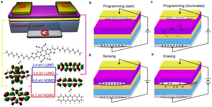
Figure 1a shows a schematic illustration of LCOM, which takes similar configuration with organic thin film transistor (OTFT). For programming, the gate electrode is positively biased (Fig. 1b,c). In dark, the bulk density of electron charge carriers in pentacene layer is very low as pentacene to be hole-dominated p-type semiconductor. In addition, electron injection from gold into pentacene is also limited because of the energy mismatch between the gold work function (WF of gold = 5.2 eV) and the LUMO of pentacene (2.4 eV, Fig. 1a)17,18. As a result, the applied positive gate voltage will not lead to charge transfer between M-C10 memory layer and pentacene layer theoretically (Fig. 1b). Then, if the device is illuminated, photo-excited electrons will come into being in pentacene (Fig. 1c). Motivated by positive gate voltage, these electrons transport towards pentacene/M-C10 interface and eventually flow into the memory layer because of the low-lying LUMO energy level of M-C10 compared with that of pentacene (Fig. 1a).
Figure 1. Schematic diagram and operational principle of LCOM.
(a) Device configuration of LCOM and the molecular structures of materials used as semiconductor and charge storage layer. HOMO-LUMO energy levels and electronic structures are determined by density functional theory calculations at the B3LYP/6-31G(d) level of theory. The device uses silica as dielectric layer (300 nm). Source−Drain electrodes are made of gold while heavily doped silicon as gate electrode. Electrical field assisted electron injection from pentacene into memory layer as the device is: (b) In dark. (c) Illuminated. The photo-excited electrons in pentacene would transport into the memory layer and stay there. (d) Device operated in TFT mode as holes accumulate at the pentacene/M-C10 interface. (e) Electric field assisted hole injection from pentacene into M-C10 when the gate voltage is enough negative. This could be recognized as an erasing process.
The photo modulated electrons stay in the memory layer and induce holes in the neighboring pentacene film. As a result, the analogue signal recorded by M-C10 is ready to be non-destructively sensed by measuring LCOM in TFT mode (Fig. 1d and Supplementary Fig. S1,S2). Comparison test based on pentacene only device without M-C10 are also performed and the results are provided in Fig. S3, S4. As we anticipated, the pentacene only device showed light sensing during illumination, but the current response disappeared immediately when the light was off. More discussion of the operating principles of an OTFT can be found in relevant review articles19,20,21. It is worth noting that if the gate voltage is enough negative, holes at the interface can also overcome the energy barrier and transport into the M-C10 layer with the aid of electrical field22. When this happens, the stored electrons will be neutralized by holes and the erasing process has been described as Fig. 1e.
Device performance of LCOM on annealed M-C10 layer
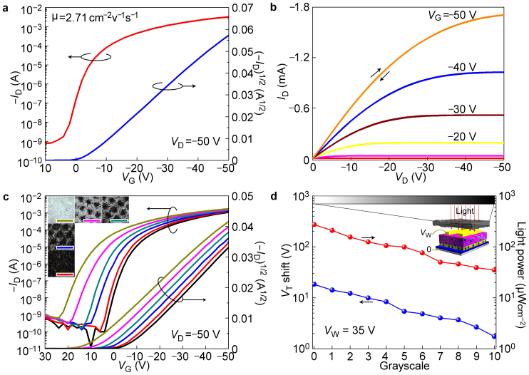
Before the deposition of pentacene, the M-C10 layer has been annealed at 80°C on hotplate for 60 seconds. It is essential to note that annealing process was a critical factor for successfully realizing the designed functionality of LCOMs (detail discussion provided later). The transfer and output curves of LCOM in TFT mode are shown in Fig. 2a,b. Better than expected, the mobility of pentacene on annealed M-C10 modification layer reached a peak value of 3.3 cm2V−1s−1 as calculated from the saturation region of transfer curve (Fig. 2a). High mobility will result in current-measuring more sensitive to the same electron density in memory layer and enable faster device switching in circuit.
Figure 2. Electrical property in TFT mode and light-controlled programming.
(a) Transfer curve and (b) Output curve of pentacene TFT using annealed M-C10 as modification layer. (c) Transfer curves before and after different doses of light exposure, which is tuned by gray papers with different grayscales. Inset: microscopic images of gray papers. (d) The linear relationship between VT shift and incident light power. Inset: schematic diagram of the measurement procedure. The light power through gray papers has been calibrated by a light intensity meter.
As a characterization of programming, the relationship between transfer curve shift and incident light power is summarized as Fig. 2c (also see Supplementary Fig. S5). During light exposure, the writing voltage (VW) was applied 35 V and 8 s while light power was controlled by means of gray paper with different grayscales. Micrographs and photographs of the gray papers are shown in Supplementary Fig. S6,S7. After exposure, the threshold voltage (VT) shift as a function of incident light power is superimposed in Fig. 2d. It is obvious that there exists a linear correlation between VT shift and light power.
One may argue that 8 s writing voltage is too long for imaging. However, the long time is deliberately chosen to make the transfer curves in Fig. 2c distinguishable to the naked eye. We have shown that a 250 ms voltage pulse is enough to induce the conductance variation of the pentacene layer at least (Fig. S2). If the exposure time for imaging was assumed to be texpo, the time required for pixels addressing and information reading was assumed to be tread, while the current for the photo-induced electrons injection into the memory layer is Iexpo, and the escaping current of stored charges is defined to be Iesca. There is an equation to realize the imaging without distortion:
So it is obvious that texpo is restricted by tread, Iesca and Iexpo. And this equation points out how to improve the refresh frequency of LCOM arrays in future.
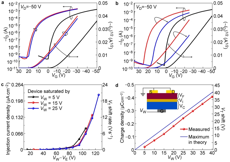
In the case of annealed M-C10 as memory layer, the stored charge retained for a long time as shown in Fig. 3a. Charge retention tests were performed by measuring the VT shift after storage for 20000 s in air. The VT was initially moved from −11.1 V (black lines) to 11.1 V (red lines) by light exposure. After 20000 s, the value of VT degraded to 9.4 V (blue lines) as determined by Fig. 3a. As VT is linearly dependent on the electron density in memory layer, the calculated charge retention ratio of 92% after 20000 s is much better than previously reported organic charge memory based on polymeric materials and represents an outstanding progress in the field of organic nonvolatile memories23,24.
Figure 3. Electrical characters of LCOMs.
(a) The transfer curve evolution after storage for 20000 s as the gate voltage was kept at 0 V. As calculated, 92% of the charges in the memory layer retained after storage for 20000 s. The trapped charges escaped at an average rate of 9.3×10⁻¹³ A cm−2. (b) The transfer curve evolution after a 0.5 s erasing voltage (VE) pulse of −100 V. (c) Plot of average hole injection current (the number equals to the rate of electrons flowing out but opposite in direction) versus erasing voltage (VE) for devices saturated by different writing voltage (VW). (d) The calculated maximum electron density under different writing voltage (VW) and the measured results. Inset: voltage distribution across the device as the gate voltage was positively biased (VW).
Besides the excellent retention property, the stored charges were also be erased in a controllable manner22. As shown in Fig. 3b, voltage pulse (−100 V, 0.5 s) was applied on gate electrode as erasing voltage (VE) in order to move the transfer curve to the negative direction and erase the recorded light signal. After erasing pulse, VT changed from 14.4 V (red lines) to 4.3 V (blue lines), and the transfer curve became close to the initial stage (black lines). To further investigate erasing process, the erasing rate dependence on VW−VE (see Fig. 3c and Supplementary Fig. S8) was also studied. We should note that the value of VW−VE represents the voltage drop across the M-C10/pentacene interface when VE was applied on the gate electrode (see Fig. S9). It was found that the VT shift was not observed when the value of VW−VE was less than 70 V. However, the erasing speed increased significantly if the absolute value of VW−VE exceeded 80 V (Fig. 3c). We should also note that the erasing process could be viewed as a tunneling process between two conjugated molecules. Similar charge transfer behavior could also be found in organic pin diodes25.
In the erasing process, there might be two ways for the electron transfer across the pentacene/M-C10 interface: (1) the positive holes injected into the memory layer and recombined with stored electrons in the LUMO energy level eventually; (2) Stored electrons in the memory layer released into the channel and recombined with the holes in pentacene26. At a given VW−VE, the total electron release current of the 2nd pathway should depend on the stored electrons density. As shown in Fig. 3d, the stored electron density in M-C10 layer is quite different for device saturated with VW of 25 V, 15 V and 5 V, while the erasing rate is similar for these devices under the same value of VW−VE (Fig. 3c). So this observation suggests that the 1st pathway might be dominated in the erasing process, although pathway 1st and 2nd are both possible in theory26. The schematic diagram and more detail explanation could also be found in Fig. S9.
In the writing process, because pentacene is a hole-dominated semiconductor, electrons will not accumulate at the M-C10/pentacene interface and so, when the gate electrode is positively biased, a positive electric field will form all across the pentacene channel area rather than being focused on the interface (Fig. 1b). The electric field in the pentacene layer provides driving force for photo-excited electrons to move towards the M-C10 layer. As electrons accumulate in M-C10 layer, the electric field in pentacene will become weaker and weaker. Eventually, photo-excited electrons cease to move. In this case, the LCOM is thought to be saturated by light under the given VW (Supplementary Fig. S10).
This process can also be described by the following equation,
Where VC is determined by the electron density in the memory layer and the specific capacitance of the dielectric layer, VI is the voltage across the pentacene/M-C10 interface, and VF is the voltage-drop in the pentacene film, which is assumed to be zero for a saturated LCOM. VC is obtained by calculating the difference ΔVT before and after light exposure. Assuming that VI is near-zero in the perfect state, the theoretical maximum charge storage of the M-C10 layer is given by VW × 11 nF cm−2 (where the latter value is the specific capacitance of the 300 nm SiO2 dielectric layer). The difference between the theoretical and measured maximum storage is determined by the actual value of VI. For the interface between pentacene and M-C10, the value of VI is only 2–3 V according to Fig. 3d, suggesting very efficient electron transfer from pentacene to M-C10 in the writing process. The small voltage drop across the interface also provides a method to refresh the device: the device was first over-erased and then saturated by a low VW (for example, 5 V). So the devices in an array can be set an initial stage regardless of their history.
Now it is clear that the LCOM could be written and erased by voltage programs, so the write-read-erase-read cycles for the LCOM as a light-assisted non-volatile memory were also tested and supplied in Fig. S11. After 1000 cycles, the on-off ratio was still larger than 103.
Influence of molecular organization and interface property on device performance
For further improvement of LCOMs, the mechanism of charge transfer between the heterojunction of pentacene and the memory layer must be explored in depth. As a main advantage compared to polymer, the molecular structure and the packing motif of small molecules in film is easier to study. In preceding paragraphs, we demonstrated that annealed M-C10 be suitable for constructing the transistor with designed functionality. Besides these results obtained using annealed M-C10, non-annealed M-C10 layer and M-C0 layer, which has identical conjugated core with M-C10 molecule but without alkyl chain substitution, were also used in the same device configuration to evaluate the device performance.
Both M-C10 and M-C0 molecules consist of inseparable mixtures of the syn- and anti-isomers, which does not considerably interfere with crystallization or X-ray diffraction studies. For the sake of simplicity, only the chemical structure of the anti-isomer is drawn in the figures of this article. The formal names and synthesis details of M-C10 and M-C0 are given in the Supplementary Information. The HOMO and LUMO energy levels of M-C10 and M-C0 molecules are close to each other according to their UV−vis absorption spectra and cyclic voltammetry (CV) measurements (Supplementary Fig. S12). The long alkyl side chains attached to the conjugated core could enhance the solubility of M-C10 compared with M-C0, so large-area uniform thin films of M-C10 were easily prepared by spin-coating while M-C0 memory layer was only fabricated by vacuum-deposition. Besides solubility enhancement, the long alkyl side chains also enable the material to undergo self-organization on annealing as shown in Supplementary Fig. S13,S14.
Both M-C0 and non-annealed M-C10 modification layers displayed clear field effect behavior (Supplementary Fig. S15), however, the mobility was much lower than that of annealed M-C10 layer as shown in Table 1. It is now well established that high mobility (μ) means the formation of excellent interface between the dielectric layer and semiconductor layer with lower density of charge traps. So the trend is clear that the trap density at the interface of annealed M-C10 layer and pentacene is much lower than that of non-annealed one, while the non-annealed M-C10 has a better interface compared with M-C0, which does not possess alkyl chains. The atomic force microscopy (AFM) was employed in the tapping mode to image the topography of three kinds of modification layers. Insight into the morphology of pentacene grown on these modification layers is also provided in Fig. S16. It is found that the topographic patterns for these three kinds of modification layers with and without pentacene grown on top were not clearly correlated with the thin film transistor performance. The most smoothing film of non-annealed M-C10 shows a moderate transistor performance. Previous reports have indicated that a rough substrate results in low mobility and high hysteresis27. However in this case of M-C10 modification layer, the pentacene mobility was larger on annealed and rough M-C10 surface than that on non-annealed and smoothing M-C10 surface.
Table 1. Pentacene TFTs performance on different modification layers.
| Pentacene on | Mobility (cm2 V−1 s−1) | Threshold voltage (VT) | On/off ratio | Subthreshold slope (S) (V decade−1) |
|---|---|---|---|---|
| M-C0 | 0.072 | −5.9 | 2.6×10⁴ | 3.30 |
| Non-annealed M-C10 | 1.04 | −1.08 | 1.5×10⁴ | 3.68 |
| 80°C annealed M-C10 | 2.74 | −1.95 | 5×10⁶ | 1.79 |
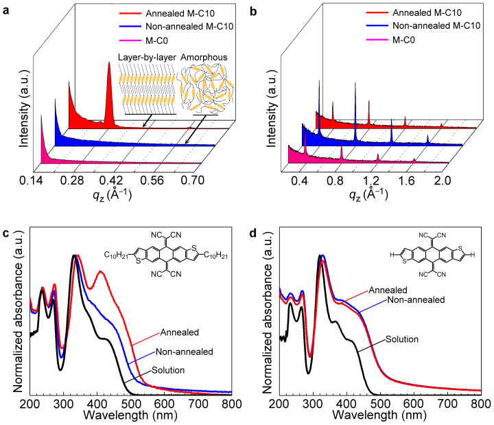
The molecular packing properties of the memory layer and the semiconductor layer were also investigated by X-ray diffraction (XRD). As shown in Fig. 4a, the non-annealed M-C10 thin film was amorphous. After annealing for 60 s at 80°C, the film showed a strong diffraction peak corresponding to a spacing of 21.5 Å, suggesting layer-by-layer packing motif which has also been evidenced by AFM image in Fig. S16. For the definite understanding of the XRD results, we grown M-C10 single crystals by slow-evaporation method using toluene as solvent and obtained the molecular packing property through X-ray analysis. The single crystal structure is shown as Supplementary Fig. S17 and the z-axis spacing distance is ca. 29.5 Å. It is obvious that the molecular organization in annealed M-C10 film is similar but not identical to that in single crystal, so the annealed M-C10 film could be described as a thin film phase. More detailed discussion including grazing incidence X-ray diffraction (GIXRD) could be found in supplementary information.
Figure 4. XRD and UV−vis absorption of the modification layers.
(a) XRD patterns of the M-C10 thin film before and after annealing, together with that of M-C0 film obtained by vacuum-deposition. The M-C10 molecules adopt a layer-by-layer packing motif in annealed thin film as evidenced by the diffraction peak appears after thermal treatment. Inset: schematic diagram of molecular packing styles of amorphous and thin film phase. (b) XRD characterization of pentacene grown on M-C0, non-annealed M-C10, and annealed M-C10 modification layers. UV−vis absorption spectra of (c) M-C0 and (d) M-C10 in solution and thin film states (before and after annealing). Inset: molecular structures of M-C10 and M-C0.
In thin film phase, the M-C10 molecules also adopt layer-by-layer packing motif. This is confirmed by GIXRD measurements in both in-plane and out-of-plane scanning motifs (Supplementary Fig. S18). For M-C10 with alkyl substituent at both ends, the layer-by-layer packing motif results in a microstructure with the long alkyl chains pointing out from the substrate plane (as depicted in the inset of Fig. 4a). In other words, the organized long alkyl chains at the M-C10/pentacene interface isolate the conjugated core of M-C10 from the pentacene semiconductor after the annealing process. The XRD patterns of pentacene films on M-C0, non-annealed M-C10 and annealed M-C10 showed the same crystalline phase (see Fig. 4b). And as the HOMO−LUMO energy levels were almost identical for M-C10 and M-C0, so the device performance variation could be ascribed to the interface difference between pentacene and modification layers.
Since UV−vis absorption spectroscopy is an effective probe of molecular aggregation, spectra of M-C10 and M-C0 were recorded to assess the extent of self-organization during thermal treatment as supplied in Fig. 4c,d. When M-C0 was annealed at 80°C in air, its UV−vis absorption property was not affected. This is not surprising as differential scanning calorimetry (DSC) measurements showed that there is no phase transition peak for M-C0 below 220°C (Supplementary Fig. S13). Meanwhile, for M-C10 a new peak appeared at long wavelength, with its position close to the maximum absorption peak of polycrystalline thin film obtained by dip-coating M-C10 from toluene (Supplementary Fig. S19). The significant difference in UV−vis absorption between the solution and the annealed thin film of M-C10 suggested that molecular reorganization occurred on thermal treatment.
The presence of self-assembled alkyl chains at the interface between dielectric and semiconductor has been reported to reduce the carrier trap density and improve OTFT performance28,29. Our observation in the case of annealed M-C10 modification layer is in good agreement with these previous contributions. The same phenomenon was also observed using a different p-type semiconductor, copper phthalocyanine (CuPc). The mobility of the CuPc OTFT increased from 5.8×10⁻⁴ cm2V−1s−1 on a bare silica substrate to 5.0×10⁻³ cm2V−1s−1 using non-annealed M-C10 as modification layer, and further increased to 2.4×10⁻² cm2V−1s−1 when incorporating annealed M-C10 layer (Supplementary Fig. S20).
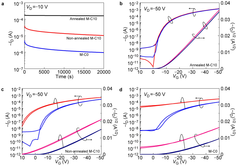
Here we should note that the self-organized alkyl blocking layer from annealing not only enhanced the thin film transistor performance, but also prolonged the charge retention time of the memory film. The source-drain current retained 92% of its initial level even after 20000 s when the annealed M-C10 film was employed. However, when M-C0 and non-annealed M-C10 films were used, the photo-generated charge stored in the memory layer was lost much more rapidly, with only 25% and 18%, respectively, of the current being retained after 20000 s (Fig. 5a). Thus, in the case of annealed M-C10 film, the well-organized alkyl chains at the surface are viewed as a dielectric layer which electrically isolates the trapped charge from the semiconductor, and this assumption is in good agreement with previous contributions emphasizing the dielectric property of self-assembling alkyl chains30,31.
Figure 5. The LCOM performance affected by interface properties.
(a) Current decay test of LCOMs with the annealed M-C10 film, non-annealed M-C10 film and M-C0 film as the memory layer after the same dose of light exposure. For annealed M-C10 memory layer, the current decreased to 92% of the initial level after storage for 20000 s; the current decayed to 25% and 18% of the initial values, respectively, for non-annealed M-C10 and M-C0 memory layers. The background transfer curve shifts when a writing voltage of 35 V was applied to the device for 60 s in dark for (b) Annealed M-C10 memory layer. (c) Non-annealed M-C10 memory layer. (d) M-C0 memory layer. The background current density in dark was significantly reduced from 3.03 nA cm−2 to 0.175 nA cm−2 after the alkyl side chain self-organization at the interface of pentacene/M-C10.
Another key parameter for LCOM is the background electron injection current into the memory layer under a positive gate voltage in dark. As a donor−acceptor (D−A) pair, charge transfer will occur if pentacene molecule and the conjugated core of M-C10 molecule are close to each other. When a positive writing voltage (VW) is applied to the LCOM, the electron–hole pairs generated at the interface will be separated by the electrical field and result in a transfer curve shift in the dark32. This background electron injection into the memory layer has a deleterious effect on the detection of weak light and should be eliminated.
According to the Marcus electron transfer theory, the self-assembled alkyl spacers between pentacene and M-C10 efficiently decrease the charge transfer probability. Indeed, as shown in Fig. 5b the dark current generated at the interface was very limited for the annealed M-C10 memory layer even when the VW of 35 V was maintained for 1 minute—the background electron injection current density was calculated to be only 0.175 nA cm−2 for the annealed M-C10 layer, whereas a much higher value of 3.03 nA cm−2 was observed with a non-annealed M-C10 layer (Fig. 5c). As for M-C0 layer, this value was even larger, reaching 3.5 nA cm−2 in average as determined from Fig. 5d. In any case, the mobility enhancement, background current reduction and prolonged charge retention time should be expected to result from the self-organization process of the memory layer and the alkyl chains packing at the interface.
The application of LCOM fabricated on large-area and flexible substrate
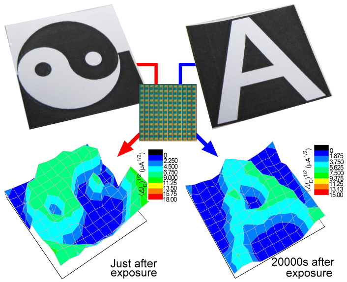
Because the devices possess the features of light-sensitivity, non-volatile memory, and non-destructive reading, and can be refreshed, we tried to fabricate a 12×12 imaging matrix on a 5×5 cm2 silicon wafer. The source electrodes of all 144 devices were connected together and grounded (inset of Fig. 6). Before imaging, the LCOMs were saturated by a VW of 5 V in 890 μW illumination for 5 s in order to set the “zero” stage of the imaging circuit. The matrix was then covered with a sheet of paper bearing a Chinese “taiji” pattern as shown in Fig. 6. After light exposure, we measured the I−V curve of every imaging pixel manually and compared them with the I−V curves of the “zero” stage. The optical information on the paper was successfully transferred to the LCOM matrix in the form of current variations. The information could be erased by applying a pulse of negative gate voltage. Then the circuit was saturated by VW of 5 V in order to refresh. Another feature, the letter “A” was also efficiently recorded by the LCOM scanner. As shown in Fig. 6, we found that the light information had been stored firmly in the memory material in the form of conductance pattern and the image was read 20000 s after light exposure.
Figure 6. Large-area imaging array constructed by LCOMs.
For the “taiji” graph, the image was collected immediately after light exposure, while for the “A” image, the conductivity pattern was measured 20000 s after light exposure. Inset: photograph of the LCOM arrays on silicon wafer.
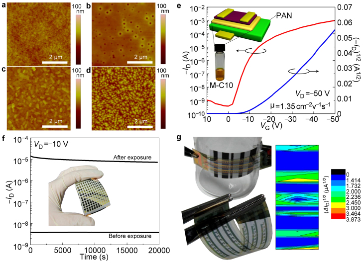
Organic electronic devices are realized on plastic substrate and this is one of the main advantages of organic materials. Here we also fabricated LCOM on poly(ethylene terephthalate) (PET) substrate. The morphology evolvement upon the fabrication steps were supplied in Fig. 7a–d. The pentacene mobility was ca. 1.35 cm2V−1s−1 as determined by the transfer curve (Fig. 7e) and the charges in the memory layer which was deposited on PAN could also be firmly stored as shown in Fig. 7f, while the on/off window remained larger than 103 after 20000 s.
Figure 7. LCOMs fabricated on flexible and large-area PET substrate.
The film morphology of (a) PAN dielectric layer. (b) M-C10 layer without thermal treatment after spin-coating. (c) Annealed M-C10 layer on PAN. (d) 40 nm pentacene grown on annealed M-C10 memory layer. (e) Transfer curve of pentacene TFT fabricated on PAN and M-C10 layer. (f) Non-volatile memory property of LCOM on PET substrate. (g) The outcome of the reading process with the LCOM array in bent status as a flexible bar code scanner and the measurement schematic diagram with bar code attached to the curved surface of a beaker.
After the above device property investigation, we fabricated a 3×24 LCOM array on PET substrate. A photograph of the resulting large-area and flexible scanner is shown in Fig. 7g. As illustrated in the inset of Fig. 7g, the imaging array could be bent to the radius of a beaker and still read a black-and-white bar code (Fig. 7g). Detail I–V curves of pixels fabricated on silica and PET substrate are provided in Supplementary Fig. S21–38.
Discussion
Although small molecular semiconductors have been widely investigated as the charge transport layer in thin film transistors and solar cells, small molecules designed as memory materials have rarely been reported until now32,33. The charge storage mechanism of M-C10 is different from existing non-volatile memory systems based on metal nanoparticles, organic donor−acceptor blends, dielectric polymers, ferroelectric transistors and floating gate memory34,35,36,37,38,39. Particularly, there are four important features of this small molecular memory material: (i) low electrical conductivity in thin film, (ii) narrow bandgap between HOMO and LUMO energy levels, (iii) efficient isolation of the conjugated core of the memory layer from the semiconductor molecules and (iv) low-lying LUMO energy level compared to the coupling semiconductor.
In detail, the low electrical conductivity allows charges to be located without flowing along the continuous spin-coated memory film. The relatively narrow bandgap guarantees that both electrons and holes can be injected into the memory layer, so that the light information can be written by a positive voltage and be easily erased by a negative voltage. The electrical isolation effect prevents the undesirable charge transfer at the interface in dark, and keeps the stored charge from escaping into the semiconductor layer. As an electron-acceptor, electrons in the neighboring semiconductor easily transport into the memory layer and tend to stay there rather than escaping back to the semiconductor. In addition to the energy level alignment of the conjugated cores, our results have shown that the presence of self-organized alkyl chains also significantly alters the electrical properties of the donor/acceptor interface.
In conclusion, we fabricated light-charge organic memory based on solution-processed charge storage small molecules and demonstrated its application on large-area and flexible substrate. Given the diversity of organic molecules, further improvements are clearly feasible through molecular design. The invention of LCOM makes one-photosensor-one-memory strategy very attractive for the realization of organic imaging circuits. More importantly, our results highlight that the use of tailored organic materials for the realization of new organic devices with a specific function offers a promising path for the future development of organic electronics.
Methods
Materials and film deposition
Polyacrylonitrile and pentacene were purchased from Aldrich Chemical. M-C10 and M-C0 molecules were synthesized according to the procedure provided in supporting information. The modification layer of M-C10 was spin-coated from a 4mg/ml chloroform solution. Pentacene layer and M-C0 layer were thermally deposited at a base pressure of 4×10⁻⁴ Pa.
Fabrication process of LCOM on PET substrate
polyacrylonitrile (PAN) thin film was spin-coated as dielectric layer. Then M-C10 memory layer was deposited onto PAN and also underwent a self-organization process by thermal treatment. As active layer in TFT, 40 nm pentacene was vacuum deposited. At last, 30 nm gold was vacuum deposited as source-drain electrodes to finish the device fabrication.
Device measurement
All electrical measurements were characterized using a Keithley 4200 semiconductor characterization system in air. The mobility in the saturated regime was extracted from the following equation: ID = Ciμ(W/2L)(VG−VT)2, where ID is the drain current, Ci is the capacitance per unit area of the gate dielectric layer, and VG and VT are the gate voltage and threshold voltage, respectively.
Author Contributions
L.Z. and Y.Q.L. designed the concept. T.W. designed and synthesized the material. L.Z. and T.W. performed the experiments and co-wrote the paper. Y.Z., X.N.S., Y.G.W., Y.L.G. and G.Y. assisted with the experiments, discussed the results and commented on the manuscript. Y.Q.L. supervised the project and finalized the manuscript.
Supplementary Material
For publication
Acknowledgments
We thank Beijing Synchrotron Radiation Facility (BSRF) for GIXRD measurements. We thank Dr. Jianming Chen and Prof. Zhigang Shuai for molecular modeling. This work was supported by the National Basic Research Program of China (2011CB932700, 2011CB808403, 2011CB932303, 2009CB623603), the National Natural Science Foundation of China (61101051, 61171054, 20973184, 20825208, 60911130231), and the Chinese Academy of Sciences.
References
- Gelinck G. H. et al. Flexible active-matrix displays and shift registers based on solution-processed organic transistors. Nature Mater. 3, 106–110 (2004). [DOI] [PubMed] [Google Scholar]
- Sekitani T. et al. Stretchable active-matrix organic light-emitting diode display using printable elastic conductors. Nature Mater. 8, 494–499 (2009). [DOI] [PubMed] [Google Scholar]
- Sekitani T. et al. Organic nonvolatile memory transistors for flexible sensor arrays. Science 326, 1516–1519 (2009). [DOI] [PubMed] [Google Scholar]
- Krebs F. C., Gevorgyan S. A. & Alstrup J. A roll-to-roll process to flexible polymer solar cells: model studies, manufacture and operational stability studies. J. Mater. Chem. 19, 5442–5451 (2009). [Google Scholar]
- Sekitani T., Zschieschang U., Klauk H. & Someya T. Flexible organic transistors and circuits with extreme bending stability. Nature Mater. 9, 1015–1022 (2010). [DOI] [PubMed] [Google Scholar]
- Someya T. et al. Integration of organic FETs with organic photodiodes for a large area, flexible, and lightweight sheet image scanners. IEEE Trans. Electron Devices 52, 2502–2511 (2005). [Google Scholar]
- Ng T. N., Wong W. S., Chabinyc M. L., Sambandan S. & Street R. A. Flexible image sensor array with bulk heterojunction organic photodiode. Appl. Phys. Lett. 92, 213303 (2008). [Google Scholar]
- Hu W. et al. A self-assembled nano optical switch and transistor based on a rigid conjugated polymer, thioacetyl-end-functionalized poly(para-phenylene ethynylene). J. Am. Chem. Soc. 127, 2804–2805 (2005). [DOI] [PubMed] [Google Scholar]
- Zhou Y., Wang L., Wang J., Pei J. & Cao Y. Highly sensitive, air-stable photodetectors based on single organic sub-micrometer ribbons self-assembled through solution processing. Adv. Mater. 20, 3745–3749 (2008). [Google Scholar]
- Jiang L., Fu Y., Li H. & Hu W. Single-Crystalline, Size, and Orientation Controllable Nanowires and Ultralong Microwires of Organic Semiconductor with Strong Photoswitching Property. J. Am. Chem. Soc. 130, 3937–3941 (2008). [DOI] [PubMed] [Google Scholar]
- Guo Y. L. et al. Multibit storage of organic thin-film field-effect transistors. Adv. Mater. 21, 1954–1959 (2009). [Google Scholar]
- Zhang L., Di C. A., Yu G. & Liu Y. Q. Solution processed organic field-effect transistors and their application in printed logic circuits. J. Mater. Chem. 20, 7059–7073 (2010). [Google Scholar]
- Gao X. et al. Core-Expanded Naphthalene Diimides Fused with 2-(1,3-Dithiol-2-Ylidene)Malonitrile Groups for High-Performance, Ambient-Stable, Solution-Processed n-Channel Organic Thin Film Transistors. J. Am. Chem. Soc. 132, 3697–3699 (2010). [DOI] [PubMed] [Google Scholar]
- Takimiya K. et al. 2,7-Diphenyl[1]benzothieno[3,2-b]benzothiophene, A New Organic Semiconductor for Air-Stable Organic Field-Effect Transistors with Mobilities up to 2.0 cm2 V−1 s−1. J. Am. Chem. Soc. 128, 12604–12605 (2006). [DOI] [PubMed] [Google Scholar]
- Handa S., Miyazaki E., Takimiya K. & Kunugi Y. Solution-processible n-channel organic field-effect transistors based on dicyanomethylene-substituted terthienoquinoid derivative. J. Am. Chem. Soc. 129, 11684–11685 (2007). [DOI] [PubMed] [Google Scholar]
- Subramanian S. et al. Chromophore Fluorination Enhances Crystallization and Stability of Soluble Anthradithiophene Semiconductors. J. Am. Chem. Soc. 130, 2706–2707 (2008). [DOI] [PubMed] [Google Scholar]
- Ahles M., Schmechel R. & von Seggern H. Complementary inverter based on interface doped pentacene. Appl. Phys. Lett. 87, 113505 (2005). [Google Scholar]
- Chua L.-L. et al. General observation of n-type field-effect behaviour in organic semiconductors. Nature 434, 194–199 (2005). [DOI] [PubMed] [Google Scholar]
- Horowitz G. Organic field-effect transistors. Adv. Mater. 10, 365–377 (1998). [Google Scholar]
- Facchetti A., Yoon M. H. & Marks T. J. Gate dielectrics for organic field-effect transistors: New opportunities for organic electronics. Adv. Mater. 17, 1705–1725 (2005). [Google Scholar]
- Zaumseil J. & Sirringhaus H. Electron and ambipolar transport in organic field-effect transistors. Chem. Rev. 107, 1296–1323 (2007). [DOI] [PubMed] [Google Scholar]
- Debucquoy M., Rockelé M., Genoe J., Gelinck G. H. & Heremans P. Charge trapping in organic transistor memories: On the role of electrons and holes. Org. Electron. 10, 1252–1258 (2009). [Google Scholar]
- Tseng C.-W. & Tao Y.-T. Electric Bistability in Pentacene Film-Based Transistor Embedding Gold Nanoparticles. J. Am. Chem. Soc. 131, 12441–12450 (2009). [DOI] [PubMed] [Google Scholar]
- Baeg K. J. et al. Organic non-volatile memory based on pentacene field-effect transistors using a polymeric gate electret. Adv. Mater. 18, 3179–3183 (2006). [Google Scholar]
- Kleemann H., Gutierrez R., Lindner F., Avdoshenko S., Manrique P. D., Lussem B., Cuniberti G., & Leo K. Organic Zener Diodes: Tunneling across the Gap in Organic Semiconductor Materials. Nano Lett. 10, 4929–4934 (2010). [DOI] [PubMed] [Google Scholar]
- Sze S. M. & Ng K. K. in Physics of Semiconductor Devices. 293–373 (John Wiley & Sons, Inc., 2016).
- Sun X. N., Di C. A. & Liu Y. Q. Engineering of the dielectric-semiconductor interface in organic field-effect transistors. J. Mater. Chem. 20, 2599–2611 (2010). [Google Scholar]
- Ito Y. et al. Crystalline ultrasmooth self-assembled monolayers of alkylsilanes for organic field-effect transistors. J. Am. Chem. Soc. 131, 9396–9404 (2009). [DOI] [PubMed] [Google Scholar]
- Virkar A. et al. The role of OTS density on pentacene and C-60 nucleation, thin film growth, and transistor performance. Adv. Funct. Mater. 19, 1962–1970 (2009). [Google Scholar]
- Halik M. et al. Low-voltage organic transistors with an amorphous molecular gate dielectric. Nature 431, 963–966 (2004). [DOI] [PubMed] [Google Scholar]
- Klauk H., Zschieschang U., Pflaum J. & Halik M. Ultralow-power organic complementary circuits. Nature 445, 745–748 (2007). [DOI] [PubMed] [Google Scholar]
- Park B., Choi S., Graham S. & Reichmanis E. Memory and Photovoltaic Elements in Organic Field Effect Transistors with Donor/Acceptor Planar-Hetero Junction Interfaces. J. Phys. Chem. C 116, 9390–9397 (2012). [Google Scholar]
- Tayi A. S. et al. Room-temperature ferroelectricity in supramolecular networks of charge-transfer complexes. Nature 488, 485–489 (2012). [DOI] [PubMed] [Google Scholar]
- Leong W. L. et al. Non-volatile organic memory applications enabled by in situ synthesis of gold nanoparticles in a self-assembled block copolymer. Adv. Mater. 20, 2325–2331 (2008). [Google Scholar]
- Baeg K.-J., Noh Y.-Y., Sirringhaus H. & Kim D.-Y. Controllable Shifts in Threshold Voltage of Top-Gate Polymer Field-Effect Transistors for Applications in Organic Nano Floating Gate Memory. Adv. Funct. Mater. 20, 224–230 (2010). [Google Scholar]
- Chu C. W., Ouyang J., Tseng H. H. & Yang Y. Organic donor-acceptor system exhibiting electrical bistability for use in memory devices. Adv. Mater. 17, 1440–1443 (2005). [DOI] [PubMed] [Google Scholar]
- Ouyang J. Y., Chu C. W., Szmanda C. R., Ma L. P. & Yang Y. Programmable polymer thin film and non-volatile memory device. Nat. Mater. 3, 918–922 (2004). [DOI] [PubMed] [Google Scholar]
- Singh T. B. et al. Nonvolatile organic field-effect transistor memory element with a polymeric gate electret. Appl. Phys. Lett. 85, 5409–5411 (2004). [Google Scholar]
- Kaltenbrunner M. et al. Anodized aluminum oxide thin films for room-temperature-processed, flexible, low-voltage organic non-volatile memory elements with excellent charge retention. Adv. Mater. 23, 4892–4896 (2011). [DOI] [PubMed] [Google Scholar]
Associated Data
This section collects any data citations, data availability statements, or supplementary materials included in this article.
Supplementary Materials
For publication


