Abstract
Understanding the mechanisms responsible for our sense of hearing requires new tools for unprecedented stimulation and monitoring of sensory cell mechanotransduction at frequencies yet to be explored. We describe nanomechanical force probes designed to evoke mechanotransduction currents at up to 100kHz in living cells. High-speed force and displacement metrology is enabled by integrating piezoresistive sensors and piezoelectric actuators onto nanoscale cantilevers. The design, fabrication process, actuator performance and actuator-sensor crosstalk compensation results are presented. We demonstrate the measurement of mammalian cochlear hair cell mechanotransduction with simultaneous patch clamp recordings at unprecedented speeds. The probes can deliver mechanical stimuli with sub-10 μs rise times in water and are compatible with standard upright and inverted microscopes.
Keywords: NEMS, MEMS, piezoresistive, piezoelectric, hair cell, hearing
The measurement of atomic scale forces plays a key role in numerous fields, particularly biology and surface science.1,2 There is a fundamental tradeoff between force and time resolution, with the time resolution of most instruments limited to 100 μs.3 However, there are phenomena that require the measurement and delivery of pN-scale forces with μs-scale time resolution, such as high-speed atomic force microscopy and cellular mechanotransduction.4,5 For instance, mammalian cochlear hair cells in the inner ear are capable of transducing pN-scale forces into an electrochemical signal at frequencies ranging from 1 to 100 kHz.6
Cochlear hair cells are typically investigated using a glass fiber mounted on a macroscale piezoelectric actuator.7 Optical tweezers have also been used for this task but are limited to work on isolated cells rather than intact tissue preparations.8 The characterization of outer hair cell bundle mechanics requires a flexible fiber with spring constant on the order of 1 pN/nm,9,10 while a rigid glass fiber can be used to study the transduction channel kinetics.11 In both cases the mechanical stimulation should ideally be delivered as an instantaneous step. But in practice, the stimulus band-width has been limited to approximately 2 and 10 kHz for flexible and rigid fibers, respectively, corresponding to 10-90% rise times of 150 and 40 μs.10,11 Electrical stimulation can be used to probe the lateral wall motility of isolated outer hair cells up to 100 kHz but does not address bundle mechanics or channel kinetics measurements.12 Given the exquisite speed and sensitivity of cochlear hair cells (e.g. mouse hearing extends to 80-100 kHz13), studies of their mechanotransduction have been constrained by instrument capabilities.
In order to address this technological gap, we have developed micromachined force probes with integrated actuation and sensing. Flexible probe bandwidth is increased while maintaining a fixed spring constant (≈ 1 pN/nm) through size reduction, while the rigid probe bandwidth is increased by using an on-chip piezoelectric actuator. Microfabrication brings other practical benefits. Glass probes are individually pulled and their overall dimensions and tip shape can vary considerably.7 In contrast, microscale probes can be mass produced using conventional silicon micromachining and their dimensions can be precisely defined lithographically.
Microcantilevers with integrated sensing and actuation for parallel atomic force microscopy have been reported previously,14–16 but they have been relatively large (e.g. 100 μm wide x 3 μm thick) and engineered for displacement rather than force resolution. Nanomechanical piezoresistive cantilevers with 10-100 kHz bandwidth in vacuum and pN-scale force resolution have been reported17,18 but lacked high-speed actuation and liquid compatibility for cellular measurements. In contrast, our probes are 300 nm thick, 1-2 μm wide and 30-200 μm long in order to simultaneously achieve a small spring constant (0.3-40 pN/nm), high resonant frequency in water (1-100 kHz) with low integrated piezoresistor force noise (1-100 pN). The probes integrate on-chip piezo-electric actuation, device- and circuit-level actuator-sensor crosstalk compensation and parylene passivation for experiments in ionic media.
We recently reported force probes with integrated piezoresistive sensing and thermal actuation.19 While the sensor performance matched our design goals, the thermal actuator rise time was limited to 100 μs in water due to heating of the surrounding fluid. In this letter we report new force probes that utilize piezoelectric actuation and achieve a rise time of 5 μs in water. The piezoresistive sensor is unchanged from our prior work and has a force resolution approximately four times its thermomechanical noise floor in water.
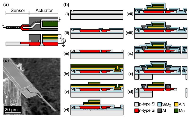
The force probe topology is presented in Figure 1a. The probe consists of a narrow, soft sensor at the tip and a wide, stiff actuator at the base. The sensor is a degenerately doped n-type piezoresistor. The actuator consists of an aluminum nitride (AlN) thin film sandwiched between two molybdenum (Mo) electrodes. Application of an electric field to the AlN actuator induces transverse motion of the force probe tip.
Figure 1.
Force probe layout, fabrication process and example device. (a) The probe consists of a narrow, soft piezoresistive sensor attached to the end of a wide, stiff piezoelectric actuator. Placement of the actuator at the base enables larger tip deflections, higher bandwidth operation and decouples the mechanical design of the actuator and sensor. (b) The probes are fabricated from SOI wafers in a nine-mask process via optical lithography. (c) SEM of a finished device. The sensor is 300 nm thick, 2 μm wide and 45 μm long with a 5.9 μm long piezoresistor while the actuator is 50 μm long and 20 μm wide.
The piezoresistor design and fabrication is unchanged from our previous devices. Briefly, the piezoresistor is designed using numerical optimization.20 The force probe numerical model includes mechanical, thermal and electrical considerations.21 The damped resonant frequency and quality factor of the first eigenmode in water are calculated from an existing model22 which we have experimentally verified.19 The piezoresistor design is optimized to minimize the RMS force noise over the intended measurement bandwidth, typically from 1 Hz to the critically damped first eigenmode, while limiting the maximum and tip temperature increases during water operation to 5 and 1 K, respectively.
The piezoelectric actuator is modeled using standard working equations.23 We opted to use AlN rather than a ferroelectric film (e.g. PZT) for process tool compatibility. We previously reported on AlN actuators with Ti electrodes24 but we switched to Mo to improve the AlN grain alignment and enable dry patterning of the piezoelectric stack. The film thicknesses in the Si/SiO2/AlN/Mo/AlN/Mo piezoelelectric stack are 300/100/25/75/75/50 nm. The silicon underneath the actuator stack is highly doped and grounded to reduce capacitive coupling between the piezoelectric actuator and piezoresistive sensor. During actuator operation the bottom Mo electrode is biased while the top Mo electrode and underlying silicon are grounded to form a coaxial structure to minimize capacitive crosstalk with simultaneous patch clamp recordings.
Two identical force probes are present on each silicon die. The main force probe is at the end of a 5 mm long extension, which enables compatibility with standard upright and inverted microscopes. The compensation force probe is set back from the tip and cancels any commonmode signals, such as crosstalk from the actuator or changes in the ambient temperature.
The probes are fabricated in the nine mask process illustrated in Figure 1b. We have previously described the piezoresistor fabrication process in detail,19 and will briefly summarize the piezoelectric-specific steps here. The process starts from a silicon-on-insulator (SOI) wafer with a 340 nm thick p-type device layer (Soitec). During the process the device layer is oxidation thinned to 300 nm. The n-type piezoresistor is formed via POCl3 predeposition. The devices are patterned via i-line optical lithography (PAS 5500/60, ASML) which limits the width of each piezoresistor leg to 500 nm and the overall width to 1 μm.
After the device layer is patterned (Figure 1b, iii) a 100 nm thick layer of low temperature oxide (LTO) is deposited using LPCVD to protect the piezoresistor during the piezoelectric stack deposition and patterning steps. Approximately 20 nm of LTO is sputtered from the wafer surface (Figure 1b, iv) before a 25 nm thick AlN seed layer, 75 nm thick bottom Mo electrode, 75 nm thick AlN actuator and 50 nm thick top Mo electrode are deposited (OEM Group). The average stress in the PE stack is adjusted to -200 ± 100 MPa in order to balance the -300 MPa stress in the underlying LTO film. The typical rocking curve full width at half maximum of the 75 nm thick AlN is 3.3 degrees.
Afterwards, the top Mo electrode is lithographically patterned and etched in SF6 plasma (Figure 1b, v). The photoresist mask is left in place and the AlN actuator is then etched in pure Cl2 with a 30 sec breakthrough step in pure BCl3.25 The photoresist is stripped and the same lithography and etch processes are repeated for the bottom Mo electrode and AlN seed layer, stopping on the underlying LTO (Figure 1b, vi). After the piezoelectric stack has been completely processed, an additional 100 nm thick layer of LTO is deposited and oxide vias are wet etched (Figure 1b, vii). The remainder of the process continues as previously described except that the Al interconnects are 400 nm rather than 1000 nm thick.19 The process yield is approximately 80% and is primarily limited by crack formation in the buried oxide.26 A finished device is shown in Figure 1c. Snap tabs are patterned into the wafer during the backside release etch, allowing the individual release of the finished die from the wafer.
The devices are epoxied to a printed circuit board (5-Minute Epoxy, Devcon) and ultrasonically wirebonded with Al wire. Wirebonding to the 50 nm thick Mo electrodes without breaking through the underlying AlN actuator can be challenging and other researchers have encountered similar problems.27 With careful optimization of the wirebonding parameters we achieved a wirebond yield of 70-80%. We would suggest adding a thick Al bondpad to future devices or using an alternative layout.28 Finally, the wirebonds are coated with the same epoxy and the entire assembly is passivated for water operation with 250 nm of parylene N.
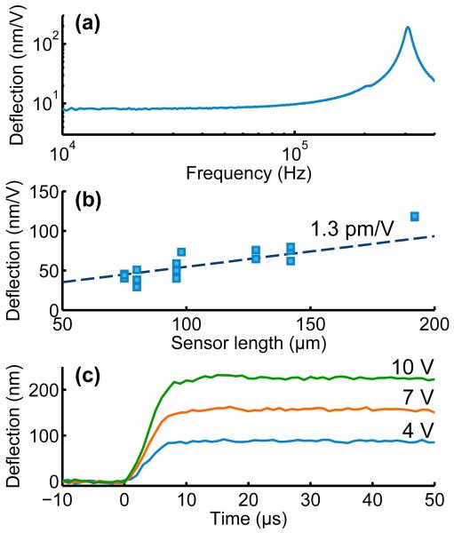
The frequency response of a force probe in air with a resonant frequency of 308 kHz is presented in Figure 2a. The actuation bandwidth is only limited by frequency response of the sensor-portion of the probe. There is a tradeoff between sensor length and tip deflection (Figure 2b). A longer sensor results in greater mechanical amplification of the actuator motion but a lower resonant frequency. Variation in tip deflection with sensor length implies an effective d31 coefficient of approximately 1.3 pm/V.
Figure 2.
Actuator performance. (a) Example frequency response in air of a force probe with a resonant frequency of 303 kHz in air. (b) Tip deflection increases with sensor length due to mechanical amplification. The effective d31 coefficient of the 75 nm thick AlN actuator is approximately 1.3 pm/V. (c) Step response in saline of a parylene passivated force probe. The 10-90% rise time is 5 μs and the tip deflection is 22 nm/V.
The step response of a passivated force probe operating in electrically grounded saline is pre-sented in Figure 2c. The probe deflection is measured by projecting its image onto a differential photodiode (SPOT-2D, OSI Optoelectronics) with a custom 230 kHz bandwidth readout circuit consisting of two transimpedance amplifiers and a differential amplifier. Compared with prior systems that worked up to 40 kHz, the bandwidth in our circuit is increased due to reductions in the amplifier gain and stray capacitance.11,29
The actuator signal is filtered at 80 kHz with an eight-pole Bessel filter (90PF-L8L, Frequency Devices). The probe response is critically damped with a 10-90% rise time of 5 μs. The resistivity and breakdown voltage of the actuator were measured as approximately 1013 Ω-cm and 10 V, respectively. The actuator is initially preloaded with a negative potential (e.g. -5 V) to maximize the single-sided deflection range.
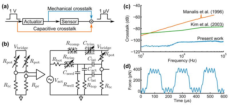
The primary downside of moving the actuator on-chip is increased crosstalk with the piezoresistive sensor. Crosstalk comes from both mechanical and capacitive sources (Figure 3a). Mechanical crosstalk is from bending of the metal interconnects that run adjacent to the piezoelectric actuator, and is limited by the gauge factor and electrical resistance of the interconnects. Capacitive crosstalk stems from coupling through the substrate and directly between the adjacent electrodes.
Figure 3.
Actuator-sensor crosstalk. (a) The piezoelectric actuator is mechanically and capacitively coupled to the piezoresistive sensor. The sensor noise floor is 120 dB smaller than the typical actuator control signal. (b) Crosstalk is converted to a common-mode signal through differential piezoresistor readout. A potentiometer and variable capacitor are used to trim mismatch between the main and compensation force probes. (c) The resulting performance is a 20 dB improvement over prior work and is limited to -115 dB by mechanical crosstalk. (d) Example of piezoresistive readout from a compensated force probe applying a 350 pN force to a hard silicon sample in air with a rise time of 10 μs and RMS force noise of 13 pN.
We combined numerous approaches to minimize crosstalk. First, we fabricated identical main and compensation force probes so that the crosstalk is primarily limited by probe mismatch. Second, we used Al interconnects to minimize the gauge factor and electrical resistance of the piezoresistor interconnects. Third, the optimal piezoresistor impedance is fairly low (2-5 kΩ) minimizing the voltage transduced by capacitive crosstalk current. Fourth, we highly doped and grounded the silicon underneath the piezoelectric actuator to provide a shunt to ground. Finally, we trimmed any capacitance mismatch between the main and compensation probes with a variable capacitor-based scheme on the printed circuit board used for sensor readout (Figure 3b).
The force probe crosstalk performance is compared with prior work in Figure 3c. Crosstalk is limited to approximately -115 dB by mechanical crosstalk and is below -100 dB to 100 kHz. The capacitive crosstalk at all frequencies is approximately 20 dB smaller than previous devices with integrated piezoresistive sensors and piezoelectric actuators.30,31 The actuator-sensor crosstalk can be comparable to the piezoresistor noise floor depending on the actuation bandwidth, deflection amplitude and sample stiffness. In Figure 3d, a force probe applies a 350 pN load to a silicon sample in air. The actuator and sensor signals are low-pass filtered at 30 kHz, yielding a rise time of 10 μs and RMS force noise of 13 pN.
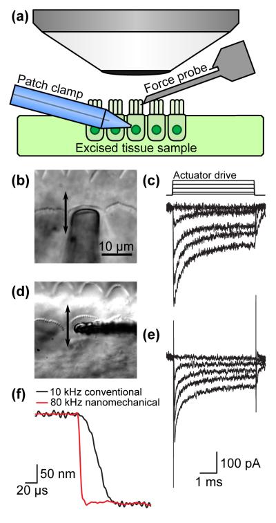
As noted earlier, the study of mammalian hearing at the cellular level is currently limited by instrument capabilities. Although hair cells have been electrically stimulated up to 100 kHz,12 direct mechanical simulation has been limited to 10-15 kHz, insufficient for the study of channel activation and bundle mechanics in the mammalian cochlea. The force probes presented here bridge this technical gap, and we have measured inner hair cell mechanotransduction using both conventional and nanomechanical probes as a demonstration experiment (Figure 4). Organs of Corti were dissected out of Sprague Dawley rats (postnatal day 6-10) and placed in our recording chamber. Tissue was dissected and perfused with pH 7.4, 300-310 mOsm external solution containing (mM): 140 NaCl, 2 KCl, 2 CaCl2, 2 MgCl2, 10 HEPES. Whole cell patch clamp (Axopatch 200B, Molecular Devices) of inner hair cells was achieved with borosilicate patch pipettes (2-3MΩ) filled with pH 7.2, 280-290 mOsm intracellular solution containing (mM): 125 CsCl, 3.5 MgCl2, 5 ATP, 5 PCr, 10 HEPES, 1 BAPTA, 3 Ascorbate. Series resistance compensation was used to increase the clamp speed of the recording. Whole cell currents were filtered at 100kHz. Current traces were filtered offline with a 4-pole 80kHz RC filter (jClamp, SciSoft Company).
Figure 4.
Comparison between conventional and nanomechanical force probes for the study of cellular mechanotransduction. (a) Experimental setup (not to scale). (b, d) Optical micrographs of the probes in the vicinity of inner hair cells from the mammalian cochlea with the movement direction indicated. (c, e) The mechanotransducer currents evoked by a step displacement are similar and adapt with similar kinetics for a constant displacement of up to 500 nm. (f) Probe step response comparison. The nanomechanical probe is nearly an order of magnitude faster than its macroscale glass counterpart.
The conventional glass probe is driven by a macroscale piezoelectric stack (AE0505D08F, Thorlabs). Although the unloaded resonant frequency of the stack is on the order of 140 kHz, the mass of the probe and compliance of the overall system limits the bandwidth to 10-15 kHz in currently published work to prevent ringing. Step waveforms are generated at 3.3 MHz using a digital to analog converter (USB-6356, National Instruments). The step is filtered using an 8-pole Bessel filter at 10kHz and variably attenuated (PA5, Tucker Davis) before being sent to a high voltage/high current amplifier to drive the macroscale piezoelectric stack. The nanomechanical force probe was driven in a similar fashion, except that the actuation signal was filtered at 80 kHz and fed into a unity gain follower (THS4031, Texas Instruments) to drive the on-chip piezoelectric actuator.
The force probe, patch clamp pipette and tissue sample are mounted on a standard upright microscope with a 60x, 2 mm working distance water immersion objective (Figure 4a). The force probe is brought into contact with an inner hair cell using a three-axis micromanipulator (MP-285, Sutter Instrument Company) before the on-chip actuator delivers a mechanical stimulus to the hair cell bundle. For this experiment, a relatively rigid force probe (45 μm long, 20 pN/nm) is used to stimulate the bundle and the probe deflection is monitored using the high-speed photodiode. The deflection of the force probe rather than the bundle was monitored as in prior work due to the obscuring presence of the probe.7 Optical micrographs of the conventional and nanomechanical force probes are presented in Figure 4b and d.
Patch clamp step-response recordings are presented in Figure 4c for the conventional probe and Figure 4e for the nanomechanical probe. The hair cell mechanotransducer currents are similar and adapt with similar kinetics to constant displacements up to 500 nm. The nanomechanical probe recordings exhibit slightly increased capacitive crosstalk (60 pA/V), which is predominantly due to the increased measurement and actuation bandwidth. The capacitive crosstalk from the conventional and nanomechanical probes are comparable (1-2 pA/V) up to 10 kHz. The nanomechanical probe increases the attainable stimulus bandwidth from 10 to 80 kHz (Figure 4f), leaving the patch clamp (≈10 kHz) as the slowest remaining component in the measurement system, suggesting that channel kinetics in the mammalian hair cell can be directly measured in the near future.
In conclusion, we have developed nanomechanical force probes with integrated piezoresistive sensing and piezoelectric actuation. The probe spring constants range from 0.3 to 40 pN/nm and are capable of delivering mechanical stimuli with sub-10 μs rise times in water. The RMS force noise of the on-chip piezoresistor ranges from 1 to 100 pN depending on the measurement bandwidth (e.g. 12 pN over 3 kHz, 36 pN over 16 kHz, 57 pN over 64 kHz) and is approximately four times the thermomechanical force noise limit in water.19 The probes are compatible with standard upright and inverted microscopes for simultaneous mechanical stimulation and patch clamp measurements of high-speed cellular mechanotransduction. These probes allow the study of apical hair bundles using mechanical stimuli whereas only electrical stimulation has been able to achieve these rates previously.12 We are currently applying the probes to the study of bundle mechanics and ion channel kinetics in mammalian cochlear hair cells. These probes are enabling fundamental observations of the mechanisms of hearing at previously inaccessible speeds and they overcome the bandwidth limitations of existing force delivery and measurement instruments through nanoscale integration.
Acknowledgement
Fabrication work was performed at the Stanford and Lurie Nanofabrication Facilities (members of the NNIN) supported by the NSF under Grant ECS-9731293. This work was supported by the NIH (R01 EB006745, RO1 DC003896, F32 DC10975 and P30-44992), the NSF (CAREER Award ECS-0449400, COINS NSF-NSEC ECS-0425914 and CPN NSF-NSEC PHY-0425897) and DARPA (YFA N66001-09-1-2089). JCD was supported in part by NDSEG and NSF Graduate Research fellowships. The authors thank A.J. Rastegar (Stanford) for helpful circuit design discussions, V. Felmetsger (OEM Group) for his expedient deposition of the AlN film stack, and S. Martin and R. Hower (U. Michigan) for performing the backside DRIE. The force probe modeling and design code is open source and available at http://microsystems.stanford.edu/piezoD.
References
- (1).Garcia R, Herruzo ET. Nature Nanotechnology. 2012;7 doi: 10.1038/nnano.2012.38. [DOI] [PubMed] [Google Scholar]
- (2).Degen CL, Poggio M, Mamin HJ, Rettner CT, Rugar D. Proceedings of the National Academy of Sciences. 2009;106:1313–1317. doi: 10.1073/pnas.0812068106. [DOI] [PMC free article] [PubMed] [Google Scholar]
- (3).Neuman KC, Nagy A. Nat Meth. 2008;5:491–505. doi: 10.1038/nmeth.1218. [DOI] [PMC free article] [PubMed] [Google Scholar]
- (4).Ando T, Kodera N, Takai E, Maruyama D, Saito K, Toda A. Proceedings of the National Academy of Sciences. 2001;98:12468–12472. doi: 10.1073/pnas.211400898. [DOI] [PMC free article] [PubMed] [Google Scholar]
- (5).Bustamante C, Macosko JC, Wuite GJ. Nature Reviews Molecular Cellular Biology. 2000;1:130–136. doi: 10.1038/35040072. [DOI] [PubMed] [Google Scholar]
- (6).Peng AW, Ricci AJ. Hearing Research. 2011;273:109–122. doi: 10.1016/j.heares.2010.03.094. [DOI] [PMC free article] [PubMed] [Google Scholar]
- (7).Crawford A, Fettiplace R. The Journal of Physiology. 1985;364:359–379. doi: 10.1113/jphysiol.1985.sp015750. [DOI] [PMC free article] [PubMed] [Google Scholar]
- (8).Qian F, Ermilov S, Murdock D, Brownell WE, Anvari B. Review of Scientific Instru-ments. 2004;75:2937–2942. doi: 10.1063/1.1781382. [DOI] [PMC free article] [PubMed] [Google Scholar]
- (9).Ricci A, Crawford A, Fettiplace R. Journal of Neuroscience. 2000;20:7131. doi: 10.1523/JNEUROSCI.20-19-07131.2000. [DOI] [PMC free article] [PubMed] [Google Scholar]
- (10).Kennedy HJ, Crawford AC, Fettiplace R. Nature. 2005;433:880–883. doi: 10.1038/nature03367. [DOI] [PubMed] [Google Scholar]
- (11).Ricci AJ, Kennedy HJ, Crawford AC, Fettiplace R. Journal of Neuroscience. 2005;25:7831–7839. doi: 10.1523/JNEUROSCI.1127-05.2005. [DOI] [PMC free article] [PubMed] [Google Scholar]
- (12).Frank G, Hemmert W, Gummer AW. Proceedings of the National Academy of Sciences. 1999;96:4420–4425. doi: 10.1073/pnas.96.8.4420. [DOI] [PMC free article] [PubMed] [Google Scholar]
- (13).Legan PK, Lukashkina VA, Goodyear RJ, Kossi M, Russell IJ, Richardson GP. Neuron. 2000;28:273–285. doi: 10.1016/s0896-6273(00)00102-1. [DOI] [PubMed] [Google Scholar]
- (14).Minne S, Manalis S, Quate C. Applied Physics Letters. 1995;67:3918–3920. [Google Scholar]
- (15).Lee KI, Takao H, Sawada K, Ishida M. Sensors And Actuators A-Physical. 2003;104:53–60. [Google Scholar]
- (16).Fantner GE, Schumann W, Barbero RJ, Deutschinger A, Todorov V, Gray DS, Belcher AM, Rangelow IW, Youcef-Toumi K. Nanotechnology. 2009;20:434003. doi: 10.1088/0957-4484/20/43/434003. [DOI] [PMC free article] [PubMed] [Google Scholar]
- (17).Harley J, Kenny T. Applied Physics Letters. 1999;75:289–291. [Google Scholar]
- (18).Arlett J, Maloney J, Gudlewski B, Muluneh M, Roukes M. Nano Letters. 2006;6:1000–1006. [Google Scholar]
- (19).Doll JC, Pruitt BL. Journal of Micromechanics and Microengineering. 2012;9:095012. doi: 10.1088/0960-1317/22/9/095012. [DOI] [PMC free article] [PubMed] [Google Scholar]
- (20).Doll JC, Park S-J, Pruitt BL. Journal of Applied Physics. 2009;106:064310. doi: 10.1063/1.3224965. [DOI] [PMC free article] [PubMed] [Google Scholar]
- (21).Doll JC, Corbin EA, King WP, Pruitt BL. Applied Physics Letters. 2011;98:223103. doi: 10.1063/1.3595485. [DOI] [PMC free article] [PubMed] [Google Scholar]
- (22).Brumley DR, Willcox M, Sader JE. Physics of Fluids. 2010;22:052001. [Google Scholar]
- (23).Weinberg M. J Microelectromech S. 1999;8:529–533. [Google Scholar]
- (24).Doll JC, Petzold BC, Ninan B, Mullapudi R, Pruitt BL. Journal of Micromechanics and Microengineering. 2010;20:025008. doi: 10.1088/0960-1317/20/2/025008. [DOI] [PMC free article] [PubMed] [Google Scholar]
- (25).Buttari D, Chini A, Palacios T, Coffie R, Shen L, xing H, Heikman S, McCarthy L, Chakraborty A, Keller S, Mishra UK. Applied Physics Letters. 2003;83:4779–4781. [Google Scholar]
- (26).Hill GC, Padovani JI, Doll JC, Chui BW, Rugar D, Mamin HJ, Harjee N, Pruitt BL. Journal of Micromechanics and Microengineering. 2011;21:087001. [Google Scholar]
- (27).Ivaldi P, Abergel J, Matheny MH, Villanueva LG, Karabalin RB, Roukes ML, Andreucci P, Hentz S, Defaß E. Journal of Micromechanics and Microengineering. 2011;21:085023. [Google Scholar]
- (28).Karabalin RB, Matheny MH, Feng x. L., Defaÿ E, Rhun GL, Marcoux C, Hentz S, Andreucci P, Roukes ML. Applied Physics Letters. 2009;95:103111. [Google Scholar]
- (29).Benser M, Marquis R, Hudspeth A. Journal of Neuroscience. 1996;16:5629–5643. doi: 10.1523/JNEUROSCI.16-18-05629.1996. [DOI] [PMC free article] [PubMed] [Google Scholar]
- (30).Manalis S, Minne S, Quate C. Applied Physics Letters. 1996;68:871–873. [Google Scholar]
- (31).Kim Y-S, Nam H-J, Cho S-M, Hong J-W, Kim D-C, Bu JU. Sensors and Actuators A: Physical. 2003;103:122–129. [Google Scholar]


