Abstract
We report the fabrication and characterization of uniformly-sized nanopore arrays, integrated into an optical detection system for high-throughput DNA sequencing applications. Nanopore arrays were fabricated using Focused Ion Beam milling followed by TiO2 coating using Atomic Layer Deposition (ALD). The TiO2 layer decreases the initial pore diameter down to sub-10nm range, compatible with the requirements for nanopore-based sequencing using optical readout. We find that the TiO2 layers produce a lower photoluminescence background as compared with the more broadly used Al2O3 coatings. The functionality of the nanopore array was demonstrated by the simultaneous optical detection of DNA-quantum dot-conjugates, which were electro-kinetically driven through the nanopores. Our optical scheme employs Total Internal Reflection Fluorescence (TIRF) microscopy to illuminate a wide area of the TiO2-coated membrane. A highly parallel system for observing DNA capture events in a uniformly-sized 6×6 nanopore array was experimentally realized.
I. Introduction
Nanopore based DNA sequencing technologies have recently made significant strides towards a full proof of principles demonstration [1]. In particular methods that employ the protein channels α-Hemolysin [2, 3] or MspA [4] show great promise due to their ability to distinguish among individual or groups of nucleotides. While protein based nanopores sequencing may perhaps be the first to reach commercial market, solid-state nanopores remain to be extremely attractive due to their superior mechanical stability and scalability [5]. Specifically, opticaly based DNA sequencing using solid-state nanopores [1, 6, 7] is viable alternative to protein-based sequencing since it straightforwardly permits parallel detection from many nanopores using high speed cameras.
To enable nucleobase-specific single-molecule fluorescence emission DNA sequencing, we recently introduced optically based DNA sequencing method, which employs solid-state nanopores [6]. The imaging system comprises of a Total Internal Reflection Fluorescence (TIRF) optics, utilizing wide-field detection of fluorescent molecules on a thin silicon nitride membrane [8]. Essential to this method is the development of a reliable fabrication method for nanopore arrays containing tens to hundreds of pores with diameter ranging between 5–8 nm and pitch at the micrometer scale.
High-resolution Transmission Electron Microscopy-based (HR-TEM) nanopore drilling methodology offers precise control of the pore size and shape. However, the HR-TEM method is not optimized for the fabrication of hundreds of pores in each chip, due to its manual, serial manner. A programmable ion beam system or an electron beam lithography system is more suitable for this application [9], [10], [11, 12]. In particular, focused ion beam (FIB) drilling is an attractive platform due to its well-established automation and the small number of process steps required, which minimizes the total fabrication time and obviates the need for etching solutions or etchant gases.
Nanopore formation using focused ion beam (FIB) milling systems has been studied by several groups [9] – [12], but reaching sub-10 nm pore dimension remains to date a challenge. Chen et al [10] showed that highly-circular pores can be drilled using a standard FIB system by depositing Pt during ion beam milling. Li et al [13] developed a method of creating nanopores with a custom-built ion beam system. This method permits an ultra-fine sculpturing of sub-5nm pores, however it is not optimized for the creation of nanopore arrays since it relies on feedback control of the ion beam from the transmitted ions. Here, we utilized a commercial dual-beam FIB for the fabrication of uniform nanopore arrays that were subsequently reduced in size using Atomic Layer Deposition (ALD) [14],[15],[16]. We illustrate the functionality of the method by optically imaging DNA capture events through the nanopore array.
II. Experimental Details
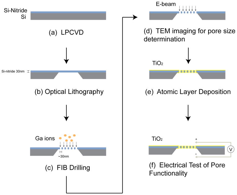
The fabrication process we employed for producing nanopore arrays is outlined in Figure 1. Silicon nitride (SiN) was deposited onto a silicon substrate using Low Pressure CVD (LPCVD) to create a low-stress nitride layer. A free-standing 30 nm thick silicon nitride membrane is fabricated using photolithography and subsequent KOH wet etching. An array of nanometer-sized pores was drilled through the silicon nitride membrane using FIB milling (Zeiss NVision 40 Dual-beam FIB-SEM system). The nanopores were drilled while injecting an H2O precursor for surface charge neutralization. The nanopore diameter was measured using a calibrated TEM (JEOL 2100 TEM).
Figure 1.
Schematic of the nanopore array fabrication process. Low Pressure CVD (LPCVD) process was employed to deposit a low-stress nitride layer above the bulk silicon substrate. A free-standing SiN membrane is fabricated using photolithography. Nanopore arrays were drilled through the SiN membrane using FIB milling. The pore size was measured using TEM. Reduction of the nanopore diameters to sub-10 nm range was achieved using ALD.
Reduction of the nanopore diameters to the desired sub-10 nm range was achieved using ALD of TiO2 (Savannah Cambridge Nanotech S200 ALD). Prior to ALD, the chips were exposed to a UV/ozone stripper to form reactive hydroxylated surfaces to create the essential surface chemistry. The silicon chip was stabilized to the targeted temperature, which in our case was varied from 175°C to 300°C, and to a chamber pressure of 450 mTorr. ALD deposition of TiO2 involves exposing the chip to a bi-sequential pulsing of H2O and titanium tetraisopropoxide Ti[OCH(CH3)2]4. Water is first pulsed for 20 milliseconds, followed by pulsing of titanium tetraisopropoxide (Ti[OCH(CH3)2]4]) (TTIP) for 300 ms. A wait time of 5 seconds between the water and the TTIP pulse is introduced to ensure that the area of interest is fully saturated with water. This facilitates adsorption of Ti atoms on the surface. Another pulsing of TTIP for 300 ms occurs prior to the next cycle to make certain that the surface reaction is completed. The number of ALD cycles is calculated based on the initial pore size and the deposition rate. The presence of TiO2 on the SiN membrane was confirmed by XPS measurement, and the final nanopore size and geometry were characterized using a TEM.
III. Results and Discussion
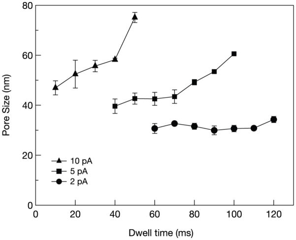
We characterized the pore size after FIB milling as a function of dwell time and ion beam current. Our results (shown in Figure 2) suggest that at 2 pA ion beam current, the pore diameter is fairly constant at ~30 nm for dwell times between 60 ms to 110 ms. It increases by ~5 nm when the dwell time is increased to 120 ms. When using ion beam currents of 5 pA or 10 pA, we observed a steep increase in the pore size as a function of dwell time. At even higher FIB currents, the ion flux resulted in an extremely rapid increase in the pore size for any practical dwell time, thus rendering this regime not useful for our application. The ion beam removes the near-surface atoms from the SiN membrane when its energy is greater than the surface binding energy of the SiN layer [17], [13]. Aside from sputtering, another process which affects the pore size is the lateral mass diffusion of atoms. The diffusion of adatoms causes the pore size to contract, and this can be observed during area scanning after drilling the pore. Scanning the membrane after a pore is formed can be employed to decrease the pore size. However, surface rippling occurs, presumably due to ion beam roughening/etching followed by relaxation from surface diffusion or viscous flow[18], and thus, is not applicable to the fine tuning of the pore size due to its low reproducibility and propensity to close the pore completely. To tune the pore size to the sub-10nm range, our approach is to add layers of TiO2 onto the SiN membrane ALD.
Figure 2.
Pore size as a function of FIB dwell time for a 30 nm-thick SiN membrane, fabricated at three different probe currents.
Atomic Layer Deposition
While ALD offers atomic-level conformality during deposition, crystalline growth at the nanopore entrance or along its sidewalls changes the contours of the pore. Titanium dioxide deposited at high temperature ALD (T ≥ 250°C) exhibits a crystalline structure. To determine the effect of ALD temperature on the pore shape, the nanopores were imaged before and after ALD, using bright-field high resolution TEM. At a deposition temperature of 300°C, the pore shape has a slight deviation from a purely conformal growth due to the crystal orientation of TiO2 (Figure 3). As the number of ALD layers increase, the crystalline structure grown on the membrane surface becomes more pronounced, altering the shape of the pore from a circular (in planar view) to a polygon-shaped pore after ALD. The crystalline structure introduces growth directionality from the nucleation site. At temperatures 210°C and 175°C, amorphous TiO2 growth was observed, and the pore shape after ALD is maintained during deposition. At a deposition temperature of 250°C, the TiO2 surface is amorphous for thicknesses < 15nm. The conformality and growth rate during ALD are influenced by saturated surface reactions and by diffusion-limited reactions inside the nanopore [19].
Figure 3.
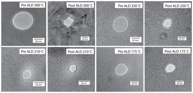
TEM micrographs of FIB-drilled nanopores pre- and post-ALD coating with TiO2 deposited at different temperatures as indicated.
Gordon et. al. derived an analytic expression for the time required to coat a pore tc, by using a simplified transport-reaction model, wherein a step function approximates the coverage inside the pore, and the propagation of the growth front is towards the bottom of the pore[20]. Their model showed that tc is a function of the aspect ratio AR of the pore, and is given by: , where S is the number of absorption site per unit area, p is the precursor pressure, m is the mass of the precursor molecule, kB is the Boltzmann constant and T is the temperature. The time required to saturate a flat surface with the precursor molecules is given by, . Using the analytic expression above, with AR = 1 (as the membrane thickness in our case is 30 nm and the initial pore diameter is ~30 nm), the nanopore can be fully coated if the time, tc is 7 times longer than that for a flat surface of the same material.
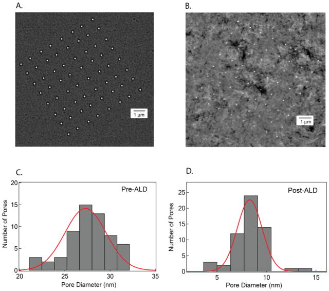
The uniformity of the nanopores in an array is characterized by measuring the pore diameter in an 8×8 array. A representative pore size distribution of an 8×8 array is shown in Figure 4, with 90% of the pores in the array being imaged using a TEM. The average pore diameter before ALD (dave) is 27.3 nm, with a standard deviation of 3.2 nm, while the average diameter post-ALD (at T = 210°C) is 8.3 nm, with a standard deviation of 1.8 nm. These measurements show that with ALD, we have a fine control on the pore dimensions, without sacrificing the number of open pores in an array.
Figure 4.
A. TEM image of an 8×8 array of nanopores, fabricated using a FIB current of 2 pA. B. TEM image of the same membrane post ALD deposition of TiO2. The pore size histograms are shown for pre- and post-ALD (C and D, respectively). Solid lines represent Gaussian fits to the distributions.
Optical Response of TiO2
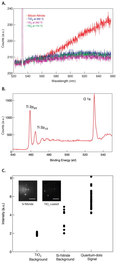
The TiO2 coating maintains the optical transparency of our free-standing membrane. Studies have shown that TiO2 on multilayer inverse opal has a relatively low luminescence [21, 22]. To investigate if the ALD-generated TiO2 is a suitable nanopore coating material for optical detection of single-molecules, we conducted optical spectroscopy studies on TiO2 deposited onto a bare silicon nitride membrane. The photoluminescence spectrum of TiO2 was obtained using a Raman Confocal Spectroscopy system (WiTEC Raman confocal microscope with UHTS 300 Spectrometer) with an excitation laser emitting at 532 nm. Figure 5A shows the photoluminescence spectra for TiO2-coated membranes processed at different ALD deposition temperatures, and for a bare SiN membrane. Our data suggests that TiO2 has low luminescence at the 580–660 nm region compared to SiN. We surmise that the low photoluminescence effect on TiO2 film is due to a low occurrence of radiative decay and radiative recombination from the Ti to O energy levels [23], as compared with SiN [24]. The bulk composition of the TiO2-coated membrane was identified using XPS (X-ray Photoelectron Spectroscopy), and the spectrum is shown in Figure 5B. A strong peak at the binding energy corresponding to the electron ejection from the Ti 2p orbital is observed in the TiO2-coated sample. The two peaks at the 460eV region show the electron ejection from the Ti 2p3/2 and Ti 2p½, and the oxygen peak is at 530eV. From this XPS spectrum, the stoichiometric film ratio of our ALD deposited TiO2 is 28.56% Ti and 71.44% O, or Ti:O2.5. We attribute the higher than expected level of oxygen to surface oxidation prior to analysis.
Figure 5.
A. Photoluminescence spectra of TiO2-coated membranes and a Silicon Nitride membrane, showing the low photoluminescence at the visible wavelength. B. XPS spectra of a TiO2-coated membrane. C. Optical background comparison between TiO2 and Silicon nitride membranes when excited by a 488 nm laser under TIRF illumination and with the emission band at 650–700 nm. The inset shows the enhancement in image contrast of the single quantum dots on a TiO2-coated membranes versus a Silicon Nitride membrane (scale bars equal 5 μm).
Another test was performed to confirm that TiO2-coated membrane can be integrated into our optical system. This involves imaging quantum dots, which were immobilized on the TiO2 membrane using a custom-built TIRF microscope [8]. The TiO2 membrane was treated with BSA-biotin to facilitate the immobilization of streptavidin-conjugated quantum dots (Invitrogen QdotR 655). The quantum dots were excited using a 488 nm laser (Coherent Sapphire 488) and its emission signal was imaged onto an EM-CCD detector (Andor DU-897), with an exposure time of 2 ms. Figure 5C shows a comparison of the optical background at the 650–700 nm wavelength from a TiO2-coated membrane and from bare silicon nitride. It also plots the optical signal from the quantum dot fluorescence. It can be seen from Figure 5C that the TiO2-coated membrane exhibits a three times improvement in the background, compared to bare Silicon Nitride membrane due to its low luminescence property.
DNA Capture in a Nanopore Array
To illustrate the functionality of the TiO2-coated nanopore arrays, we use an objective-based TIRF [8] with a 488 nm-laser to image 1 kbp ds-DNA, which was attached to a streptavidin-coated quantum dot. The quantum dot serves as an anchor to hold the DNA inside the nanopore when an electric field is applied. When an external electrical field (V = 200 mV) is applied across the membrane, the Qdot-DNA molecules are randomly drawn towards the nanopores (the concentration of Qdot-DNA molecules in the cis chamber is ~100 pM). In Figure 6, we show a representative series of images when the DNA-quantum dot molecules were trapped inside a 6×6 nanopore array. The Qdot-DNA molecules are captured in the pore, but they do not translocate through the pore, because the diameter of the quantum dot is larger than the pore diameter. Figure 6B shows a CCD image of an illuminated area in the membrane within the vicinity of the nanopore array and no electrical field is present. Since there is no applied voltage, the molecules are freely diffusing in the ionic solution. Upon application of a positive voltage, we observe clear fluorescence signals in 18 pores, indicating the lodging of Qdot-DNA conjugates in each pore. This implies that 50% of the pores in the 6×6 array were occupied by DNA strands, or the pores are completely open for the entire duration of the experiment. The location of the fluorescence spots, imaged by the EMCCD camera, corresponds to the location of the nanopores on the chip. Two adjacent nanopores in this array has a spacing of 1.5 μm. This corresponds well with the spacing between the fluorescence signals from the quantum dots. Moreover, switching off (or reversal) of the electric field resulted in the disappearance of the fluorescence signal, due to the escape of the Qdot-DNA from the nanopores (data not shown).
Figure 6.
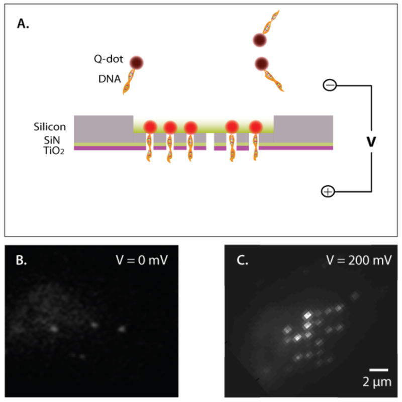
A. Schematic illustration of the TIRF based imaging of the nanopore array and Qdot-DNA conjugates. Bottom: Optical images of the membrane before (B) and after application of a positive voltage (C). The discrete fluorescent spots arise from the Qdots-DNA conjugates, exhibiting partial occupancy of a 6×6 nanopore array when a positive voltage is applied.
IV. Conclusions
In summary, we have demonstrated that uniformly-sized nanopore arrays can be fabricated using FIB drilling and subsequent ALD. A commercial FIB system can be optimized and easily automated to reproducibly create tens to hundreds of pores per chip, whose diameters can be decreased to sub-10 nm using ALD. By employing a simple, direct process for creating nanopores, we address the need for a fabrication method that is applicable to an optical DNA sequencing platform.
Optical detection of DNA molecules conjugated to Qdots was performed using 6×6 nanopore arrays. To enhance the detection capability, the nanopores were coated with TiO2 during ALD, which we have shown to produce less luminescence than silicon nitride in the 580 nm – 700 nm region. Furthermore, we have optimized the TiO2 ALD process, such that the nanopore contours remain conformal after layers of TiO2 were added to obtain the pore size significant for DNA studies. This type of nanopore array, integrated into an optical system, is a major step towards the realization of a low cost, high throughput DNA sequencing device.
Acknowledgments
We acknowledge financial support from National Human Genome Research Institute award R01 HG-005871. We acknowledge support from the Center for Nanoscale Systems in Harvard University where parts of the fabrication process were performed.
References
- 1.Branton D, et al. The potential and challenges of nanopore sequencing. Nature Biotechnology. 2008;26:1146–1153. doi: 10.1038/nbt.1495. [DOI] [PMC free article] [PubMed] [Google Scholar]
- 2.Clarke J, et al. Continuous base identification for single-molecule nanopore DNA sequencing. Nature Nanotechnology. 2009;4(4):265–270. doi: 10.1038/nnano.2009.12. [DOI] [PubMed] [Google Scholar]
- 3.Cherf G, et al. Automated forward and reverse ratcheting of DNA in a nanopore at 5-A precision. Nature Biotechnology. 2012;30(4):344–348. doi: 10.1038/nbt.2147. [DOI] [PMC free article] [PubMed] [Google Scholar]
- 4.Manrao E, et al. Reading DNA at single-nucleotide resolution with a mutant MspA nanopore and phi29 DNA polymerase. Nature Biotechnology. 2012;30(4):349–354. doi: 10.1038/nbt.2171. [DOI] [PMC free article] [PubMed] [Google Scholar]
- 5.Venkatesan BM, Bashir R. Nanopore sensors for nucleic acid analysis. Nature Nanotechnology. 2011;6:615–624. doi: 10.1038/nnano.2011.129. [DOI] [PubMed] [Google Scholar]
- 6.McNally B, et al. Optical recognition of converted DNA nucleotides for single molecule DNA Sequencing using Nanopore Arrays. Nano Letters. 2010;10(6):2237–2244. doi: 10.1021/nl1012147. [DOI] [PMC free article] [PubMed] [Google Scholar]
- 7.Singer A, et al. Nanopore-based technology: Single molecule characterization and DNA sequencing. Humana Press; Springer: 2011. DNA Sequencing by Nanopore Induced Photon Emission (SNIPE) [Google Scholar]
- 8.Soni G, et al. Synchronous optical and electrical detection of biomolecules traversing through solid-state nanopores. Review of Scientific Instrument. 2010;81:014301–014308. doi: 10.1063/1.3277116. [DOI] [PMC free article] [PubMed] [Google Scholar]
- 9.Kim MJ, et al. Rapid Fabrication of Uniform Nanopores and Nanopore Arrays. Advanced Materials. 2006;18(23):3149–3153. [Google Scholar]
- 10.Chen P, et al. Fast single-step fabrication of nanopores. Nanotechnology. 2009;20(015302):1–6. doi: 10.1088/0957-4484/20/1/015302. [DOI] [PubMed] [Google Scholar]
- 11.Wu MY, et al. TEM study of locally coated nanopore fabricated by ion-beam-induced deposition in a thin membrane. Micron. 2010;41(6):609–614. doi: 10.1016/j.micron.2010.03.009. [DOI] [PubMed] [Google Scholar]
- 12.Mussi V, et al. DNA-functionalized solid-state nanopore for biosensing. Nanotechnology. 2010;21:5. doi: 10.1088/0957-4484/21/14/145102. [DOI] [PubMed] [Google Scholar]
- 13.Li J, et al. Ion Beam Sculpting at Nanometer Length Scales. Nature. 2001;412:166. doi: 10.1038/35084037. [DOI] [PubMed] [Google Scholar]
- 14.Venkatesan BM, et al. Highly Sensitive Nanopore Sensors for DNA Analysis. Advanced Materials. 2008;21(27):2771–2776. doi: 10.1002/adma.200803786. [DOI] [PMC free article] [PubMed] [Google Scholar]
- 15.Nam SW, et al. Ionic Field Effect Transistors with Sub-10nm Multiple Nanopores. Nano Letters. 2009;9(5):2044–2048. doi: 10.1021/nl900309s. [DOI] [PubMed] [Google Scholar]
- 16.Chen P, et al. Atomic layer deposition to fine-tune the surface properties and diameters of fabricated nanopores. Nano Letters. 2004;4(7):1333–1337. doi: 10.1021/nl0494001. [DOI] [PMC free article] [PubMed] [Google Scholar]
- 17.Biersack JP, Eckstein W. Applied Physics Letters. 1984;(A34):73–94. [Google Scholar]
- 18.Erlebacher J, et al. Spontaneous Pattern Formation on Ion Bombarded Si(001) Physical Review Letters. 1999;82(11):2330–2333. [Google Scholar]
- 19.Elam JW, et al. Conformal Coating on Ultrahigh-Aspect Ratio Nanopores of Anodic Alumina by Atomic Layer Deposition. Chemistry of Materials. 2003;15:3507–3517. [Google Scholar]
- 20.Gordon RG, et al. A Kinetic Model by Step Coverage by Atomic Layer Deposition in Narrow Holes or Trenches. Chemical Vapor Deposition. 2003;9(2):73–78. [Google Scholar]
- 21.King J, Graugnard E, Summers CJ. Photoluminescence modification by high-order photonic bands in TiO2/ZnS:Mn multilayer inverse opals. Applied Physics Letters. 2006;88(081109):1–3. [Google Scholar]
- 22.Palik E. Handbook of Optical Constants of Solids. 1998 [Google Scholar]
- 23.Wang X, et al. Trap states and carrier dynamics of TiO2 studied by photoluminescence spectroscopy under weak excitation condition. Physical Chemistry Chemical Physics. 2010;12:7083–7090. doi: 10.1039/b925277k. [DOI] [PubMed] [Google Scholar]
- 24.Desphande S, et al. Optical properties of silicon nitride films deposited by hot filament chemical vapor deposition. Journal of Applied Physics. 1995;77(12):6535–6541. [Google Scholar]


