Abstract
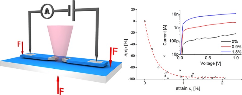
In this Letter we present the electrical and electro-optical characterization of single crystalline germanium nanowires (NWs) under tensile strain conditions. The measurements were performed on vapor–liquid–solid (VLS) grown germanium (Ge) NWs, monolithically integrated into a micromechanical 3-point strain module. Uniaxial stress is applied along the ⟨111⟩ growth direction of individual, 100 nm thick Ge NWs while at the same time performing electrical and optical characterization at room temperature. Compared to bulk germanium, an anomalously high and negative-signed piezoresistive coefficient has been found. Spectrally resolved photocurrent characterization on strained NWs gives experimental evidence on the strain-induced modifications of the band structure. Particularly we are revealing a rapid decrease in resistivity and a red-shift in photocurrent spectra under high strain conditions. For a tensile strain of 1.8%, resistivity decreased by a factor of 30, and the photocurrent spectra shifted by 88 meV. Individual stressed NWs are recognized as an ideal platform for the exploration of strain-related electronic and optical effects and may contribute significantly to the realization of novel optoelectronic devices, strain-enhanced field-effect transistors (FETs), or highly sensitive strain gauges.
Keywords: Germanium, nanowire, strain, piezoresistivity, bandgap modification
Due to the high mobility values, particularly for holes, and the compatibility with complementary metal–oxide–semiconductor (CMOS) processing, Ge has been introduced into standard Si technology since years.1 In addition, due to the small difference between direct and indirect bandgap energy, Ge appeared to be a promising material for next generation on-chip light sources and detectors2,3 and thus triggered a lot of activities for photonic applications.4−11 Thereby the main issue is to overcome the inefficient light emission of an indirect semiconductor. There have been several attempts to minimize the 136 meV gap between the direct Γ- and the indirect L-valley, including band structure modifications by quantum confinement, alloying, or strain engineering, also in combination with heavy doping. A direct band gap can be obtained by zone folding and quantum confinement by growth of alternating layers of Si/Ge. Zone-folding transitions do, however, typically show weak transition strength.12 Interalloying and strain effects are further challenges in those superlattices.13 Another approach, alloying Ge with Sn, indeed yields a direct band gap material,14 but growth appeared to be a crucial issue due to the low solubility of Sn in Ge.15 Under biaxial tensile strain conditions the conduction band lowers in energy whereby the Γ-valley lowers faster than the L-valley, and thus for strain values of about 2%16 Ge transforms to a direct bandgap semiconductor.17,18 With respect to biaxially strained layers, epitaxial growth requires host materials with a proper lattice constant, thermal expansion coefficient, and polarity. To the best of our knowledge, using sophisticated growth schemes, Huo et al. were the only ones exceeding the 2% strain hurdle for direct bandgap properties growing 2.33% tensile strained Ge layers on InGaAs buffer layers.11 Contrary to theoretical predictions they found a rather small change in the direct band gap energy, nevertheless shifting the transition out of the favorable telecom band around 1550 nm. Synthesis, however, remains the major challenge in Ge thin film growth, as thermal expansion and lattice mismatch cause a high density of interface and threading dislocations, as well as increased surface roughness.19 To circumvent the problem of growing such heavily strained layers and to keep the emission wavelength within the telecom band Liu et al. proposed a combination of moderate strain and n-type doping to enhance direct recombination in Ge.16 In-plane strain is utilized to lower the difference in energy between Γ- and L-valley. Additionally the doping raises the Fermi level closer to the Γ-valley and thus increases the carrier population. High doping, however, causes enhanced free carrier absorption.
The ability to fabricate single-crystal nanowires (NWs) that are widely free of structural defects can be employed to apply sufficiently high strain levels without the need of additional doping. In Ge-NWs, uniaxial tensile strain values of more than 10% have already been demonstrated without fatigue failure.20 Due to the low defect density along the NW, ultimate strength overcomes the theoretical limit for bulk Ge of 15 GPa. Simulation results, quantifying the amount of uniaxial strain for the indirect-to-direct transition in Ge-NWs, vary over a wide range from 1.05%21 up to 4.2%.9 This is, however, well below the demonstrated 10% fracture strength. The high strain values feasible in Ge-NWs together with the large Bohr exciton radius (24.3 nm) and carrier confinement in these quasi-one-dimensional structures make them an ideal platform for the exploration of strain-related one-dimensional light-matter interaction effects.6
Based on individual NWs monolithically integrated in a sophisticated micromechanical strain module, we explored a technique to characterize ultra-strained NWs by μ-Raman spectroscopy, conductance, and spectrally resolved photocurrent measurements. Figure 1a shows a sketch of the 3-point straining module with an individual Ge-NW bridging the Si pads of a silicon-on-insulator (SOI) device structure. As the two Si pads are electrically insulated with respect to the handle wafer this module enables I/V measurement of an individual Ge-NW under various strain conditions. The scanning electron microscopy (SEM) image in Figure 2a shows the detailed view of a ⟨111⟩-oriented Ge-NW bridging the two insulated Si pads. These pads were structured from the highly p-doped (110)-oriented device layer of an SOI wafer by photolithography and reactive ion etching. Gold colloids were placed on the ⟨111⟩-oriented sidewall facet by dielectrophoresis to act as catalyst for vapor–liquid–solid (VLS) based NW growth. Synthesis parameters were optimized to grow epitaxial, ⟨111⟩-oriented Ge-NWs perpendicular to the {111} surface of the freestanding Si pads. Further information on the synthesis process is available in the Supporting Information. The TEM images in Figure 2b and c demonstrate the epitaxial growth and the sharp interface at the Si/Ge heterojunction. The length of the NW is determined by the distance between prepatterned Si pads, which is typically 3.5 μm. Finally, the SOI chip is aligned and glued firmly onto a steel plate, and electrical contacts are formed by aluminum wire bonding to the corresponding pads as shown in Figure 1a.
Figure 1.
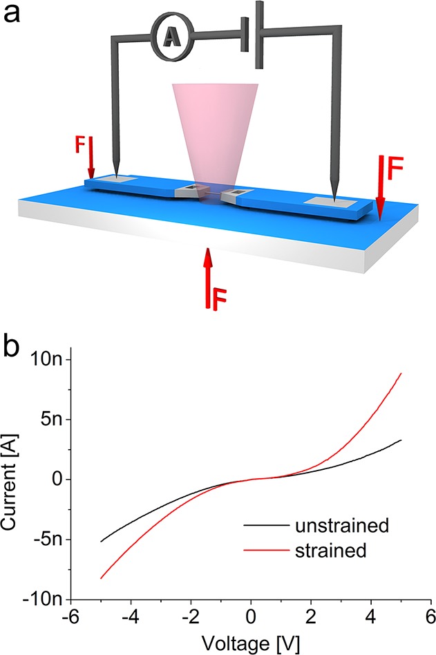
(a) Sketch of the 3-point straining module for electro-optical characterization of suspended single nanowires. (b) I/V characteristics of a Ge NW indicating space charge limited transport and increased conductivity under strain.
Figure 2.
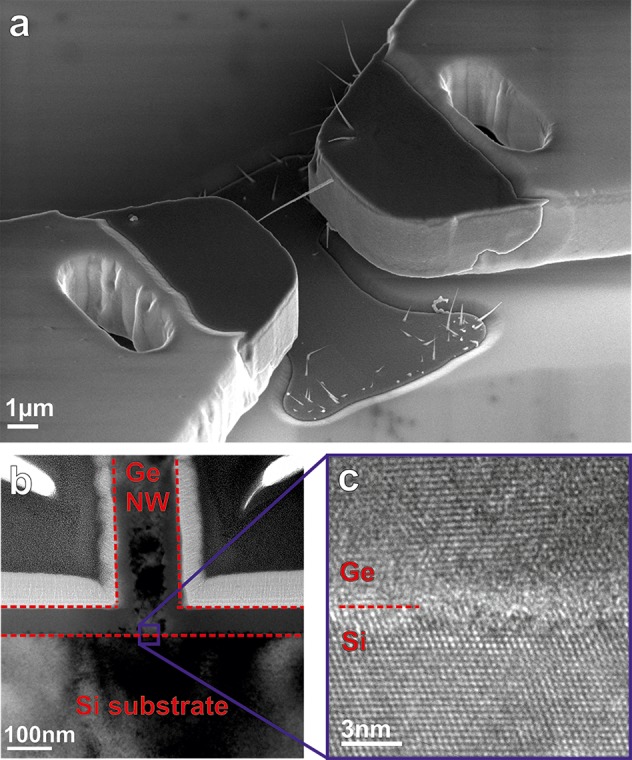
⟨111⟩-oriented Ge-NW bridge. (a) SEM image of the suspended Ge-NW aligned along the ⟨111⟩ direction, within a trench with vertical {111} facets on a ⟨110⟩-oriented SOI substrate. (b) Cross-sectional TEM image of a Ge NW with amorphous Ge shell on (111) Si substrate. To improve imaging quality, a layer of carbon and platinum was deposited on the sample. (c) HR-TEM image confirming heteroepitaxial growth of the Ge-NW on Si.
Thus, when the steel substrate is subject to 3-point bending, mainly uniaxial tensile stress is created along the NW. Stresses other than in the axial direction cannot be imposed because the NW is anchored only with its two ends at the SOI facets. Figure 1b shows typical I/V plots of a strained and unstrained Ge-NW. The S-shaped I/V characteristic indicates space charge limited transport22 with the current mainly governed by the mobility of charge carriers in the intrinsic NW.23 Increasing conductivity for increasing strain is observed. For the determination of stress we are employing confocal μ-Raman microscopy enabling in situ high spatial resolution measurements of individual strained NWs.24 Figure 3 shows the Raman spectrum of the reference bulk Ge sample and of an individual Ge-NW subject to increasing strain. Bulk Ge and unstrained NWs exhibit the first-order optical phonon peak at 300.5 cm–1.
Figure 3.
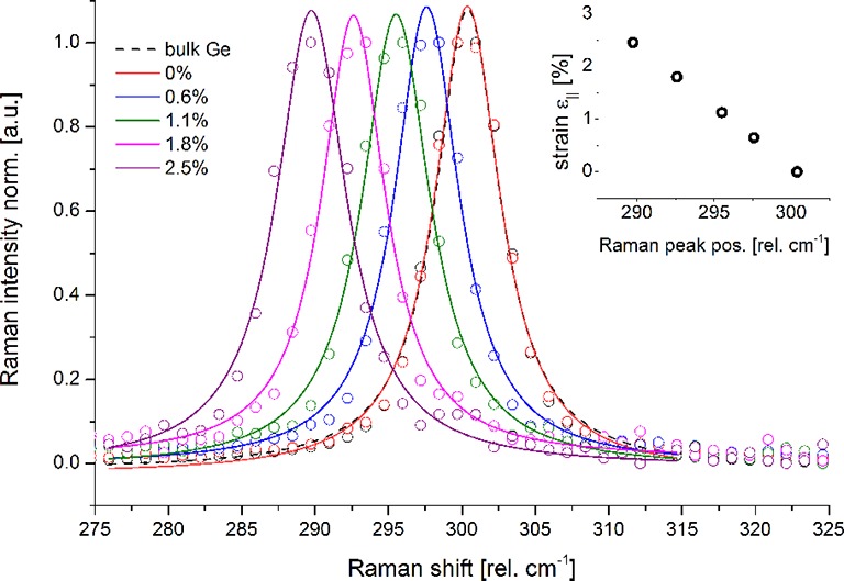
Normalized Raman spectra of one single suspended Ge NW subject to increasing strain. Under zero strain conditions the spectrum equals the one for bulk Ge. For increasing tensile strain, the spectrum shifts toward lower wavenumbers, down to 290 cm–1, corresponding to 2.5% tensile strain. The inset shows the Raman peak positions and strain values for each of the spectra.
An application of stress to the Ge-NW causes a shift linearly dependent on the strain as shown in the inset of Figure 3. The relation of the shift in the Raman spectra and uniaxial strain is given by:
With ΔΩ representing the shift in peak position, k a proportionality factor, and ε∥ the strain in ⟨111⟩ direction. We performed calibration measurements comparing Raman peak shifts with a physical length change of the NW. The length and elongation of the Ge-NW under stress was determined in situ by SEM imaging, measuring the distance between the two ends of the NW. The epitaxial growth of the Ge-NWs perpendicular to the Si pads (i.e., to the direction of the electron beam) enables a precise measurement of the NW elongation with approximately 10 nm precision without any “hidden” displacement along the electron beam direction. Our calibration measurements reveal k = 434 cm–1 and are in good agreement with bulk Ge values from Cerdeira et al. of k = 438 cm–1.25 The above equation is further used to quantify the strain level of the Ge-NWs immediately before the electo-optical characterization. Thus a peak shift of about 11 cm–1 as shown for the highest strain level in Figure 3 corresponds to a tensile strain of about 2.5%. For the electrical characterization the two electrodes of the measurement module in Figure 1a were connected to a semiconductor analyzer, and the current was measured during continuous voltage sweeps applied to the Ge-NW at different strain levels. Doing so, the local NW resistance is measured in a two point configuration with the disadvantage of the parasitic effect of the contact resistance. However, for the heavily doped electrode regions the contribution of the resistance between the electrodes and the NW was found to be negligible. Four-probe measurements of such grown Ge-NWs revealed an intrinsic resistivity of ρNW = 1–10 kΩ·cm. The conductivity-type of the Ge-NW was determined by a NW field-effect transistor (FET) with back gate geometry exhibiting a field effect response characteristic of a p-type semiconductor (see Supporting Information). This p-type behavior is a common observation for VLS-grown Ge-NWs without intentional doping.26 The inset in Figure 4 illustrates typical I/V characteristics of an unstrained Ge-NW and for strain levels of 0.9% and 1.8%. From the I/Vs the striking impact of strain on NW conductivity can be observed. While the shape of the characteristic is similar for all strain levels, the current increases over more than 1 order of magnitude for 1.8% strain. Modification of the lattice constant and crystalline structure by stress strongly affects the band structure, carrier concentration, and carrier transport properties.27 One manifestation of these altered properties of the crystal is piezoresistivity, that is, the dependency of resistivity ϱ on the stress σ within a material:
with π1 the longitudinal piezoresistive coefficient.
Figure 4.
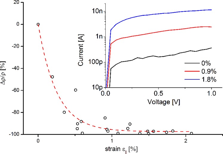
Relative change in resistivity as a function of strain. Values are extracted at bias voltages of 1 V. The data can be fitted exponentially with a piezoresistive coefficient of −249 × 10–11 Pa–1 extracted as the slope of the fit at zero strain. Inset: Typical I/(V s) under increasing strain conditions.
For p-type bulk Ge the piezoresistive coefficient in ⟨111⟩ direction was determined to be about π1 = 65 × 10–11 Pa–1 leading to an increase of the resistivity for tensile strained Ge.27 Contrary, for our heavily strained Ge-NWs we measured a remarkable decrease of the resistivity. Similar behavior was previously reported for highly strained ⟨111⟩ oriented Si-NWs.23 The work of He and Yang28 gave experimental evidence on a positive giant piezoresitance effect (PZR) in Si-NWs at lower strain levels of up to 0.04%. Their findings stimulated a lot of further theoretical and experimental research effort on piezoresistive effects in nanostructures.29−37 Although several studies have been published, there seems to be no consensus on the origins of giant PZR. Cao et al.29 proposed a strain-induced band switching between two surface states to be the main mechanism involved. Rowe30 explained giant PZR with a strain-induced increase in the width of the surface depletion region due to changes in surface charge. He and Yang28 claimed that carrier mobility is the main mechanism but also emphasized the important contribution of surface effects and carrier concentration on giant PZR. Quantum confinement as proposed by Pramanik et al.31 seems to be an unlikely explanation due to the size of the structures well above 50 nm. Milne et al.32 noted that giant PZR was only reported for depleted structures and therein resistance changes are dominated by transient electron and hole capture processes in surface traps. They showed that the trap-induced decay of current with time can be mistaken for an apparent giant PZR. Our data from time-dependent measurements, however, indicate only noisy fluctuations of current on a typical measurement time scale but no systematic deviation (see Supporting Information). In Figure 4 the relative change in resistivity is plotted as a function of strain and shows the monotonic decrease in resistivity with an exponential decay. Resistivity values are extracted at 1 V bias from different single Ge-NW devices. Dimensional changes in the NW are neglected due to their small contribution. The equation for the relative change in resistivity Δϱ/ϱ for a cylindrically shaped piezoresistive element is given by
with ν the Poisson's ratio and ε∥ the strain along the cylinder axis.
Figure 4 shows that at 0.65% strain resistivity is decreased by −90% and further decreases to −97% at the maximum value of 2.1% strain. A linear fit of the exponential decay in Figure 4 at the zero strain point yields a piezoresistive coefficient of π1 = −249 × 10–11 Pa–1 (assuming a Young's modulus of Ge along ⟨111⟩ of 155 GPa). As the discussion on the underlying mechanisms of anomalous piezoresistive effects in nanostructures is still going on, we are contributing first experimental data for Ge-NWs and emphasize on the importance of further studies to reveal the physics involved.
To probe the band modifications induced by strain more directly, photocurrent spectroscopy was used to determine the effects on bandgap energy. The inset in Figure 5 shows photocurrent spectra of a single suspended Ge-NW under increasing strain conditions. Thereby the photocurrent is given in terms of external quantum efficiency (EQE). EQE is defined as the ratio of photocurrent to the incident photon flux on the projected NW area.
In the spectrum we observe characteristic ripples, which are attributed to the specific layer structure in the SOI device (see Supporting Information). Under tensile strain, we observed a redshift in the photocurrent spectrum; that is, for increasing strain the onset of photocurrent is shifted toward higher wavelengths. The corresponding shift in energy for several devices is displayed in Figure 5 and appeared to be linearly dependent on strain
with the proportionality factor a∥ = −5.0 eV. Comparison to deformation potential theory for the direct bandgap in bulk germanium38 gives reasonable agreement, though our result is ∼23% lower than a∥dir = −6.48 eV calculated from theory for bulk material. Interpreting the shift in photocurrent spectra as a shift in direct bandgap energy, this means that the direct bandgap in the NW geometry is lowering slower with strain than assumed by theory and will be an important input parameter for future device designs as well as simulations.
Figure 5.
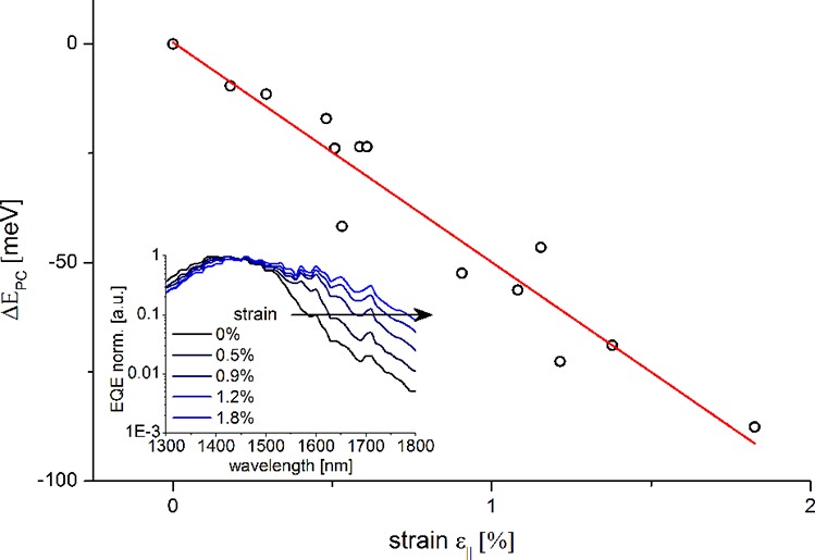
Shift in the Ge-NW photocurrent spectra as a function of uniaxial strain along the ⟨111⟩ growth direction. Values are extracted from quantum efficiency spectra of several devices. The data are linearly fitted with a slope of a∥ = −5.0 eV. Inset: Quantum efficiency spectra of a single suspended Ge-NW monolithically integrated in the straining device. Spectra are normalized to their maximum to highlight the change in shape. With increasing strain the onset of photocurrent shifts toward the red, indicating a lowering of the direct-bandgap energy.
Summarizing we have shown Raman, electrical, and optical characterization of strained Ge-NWs, revealing anomalous piezoresistive behavior, that is, a nonconstant negative piezoresistive coefficient with resistivity change being exponentially dependent on strain. Furthermore we deliver experimental data on the dependency of the shift in photocurrent spectra on uniaxial strain in the ⟨111⟩ direction. The extraordinary piezoresistive behavior of Ge-NWs could find applications in micorelectromechanical systems (MEMS) devices, strain-sensing, and high-performance CMOS devices. Our findings on the electro-optical tunability of strained Ge-NWs may contribute to a better understanding of strain induced effects in nanostructures and pave the way toward novel optoelectronic devices.
Acknowledgments
The authors acknowledge financial support by the Austrian Science Fund (FWF): projects SFB-IROn No. F2503-N17 and project No. P20937-N14. The cleanroom facilities are provided by the Center for Micro- and Nanostructures (ZMNS) Vienna. Technical support by USTEM TU Wien is gratefully acknowledged.
Supporting Information Available
Device fabrication and NW synthesis, NW FET synthesis and characterization, Raman setup, time-dependent current measurements, photocurrent spectroscopy setup, and additional information on the photocurrent spectra. This material is available free of charge via the Internet at http://pubs.acs.org.
The authors declare no competing financial interest.
Supplementary Material
References
- Song Y.; Zhou H.; Xu Q.; Luo J.; Yin H.; Yan J.; Zhong H. J. Electron. Mater. 2011, 40, 1584. [Google Scholar]
- Wang J.; Lee S. Sensors 2011, 11, 696–718. [DOI] [PMC free article] [PubMed] [Google Scholar]
- Basu P. K.; Das N. R.; Mukhopadhyay B.; Sen G.; Das M. K. Opt. Quant. Electron. 2010, 41, 567–581. [Google Scholar]
- Ahn Y. H.; Park J. Appl. Phys. Lett. 2007, 91, 162102. [Google Scholar]
- Cao L.; White J. S.; Park J.-S.; Schuller J. A.; Clemens B. M.; Brongersma M. L. Nat. Mater. 2009, 8, 643–647. [DOI] [PubMed] [Google Scholar]
- Kim C.-J.; Lee H.-S.; Cho Y.-J.; Kang K.; Jo M.-H. Nano Lett. 2010, 10, 2043–2048. [DOI] [PubMed] [Google Scholar]
- Lim P. H.; Park S.; Ishikawa Y.; Wada K. Opt. Express 2009, 17, 16358–16364. [DOI] [PubMed] [Google Scholar]
- Liu J.; Sun X.; Camacho-Aguilera R.; Kimerling L. C.; Michel J. Opt. Lett. 2010, 35, 679–681. [DOI] [PubMed] [Google Scholar]
- Zhang F.; Crespi V. H.; Zhang P. Phys. Rev. Lett. 2009, 102, 156401. [DOI] [PubMed] [Google Scholar]
- de Kersauson M.; El Kurdi M.; David S.; Checoury X.; Fishman G.; Sauvage S.; Jakomin R.; Beaudoin G.; Sagnes I.; Boucaud P. Opt. Express 2011, 19, 17925–17934. [DOI] [PubMed] [Google Scholar]
- Huo Y.; Lin H.; Chen R.; Makarova M.; Rong Y.; Li M.; Kamins T. I.; Vuckovic J.; Harris S. H. Appl. Phys. Lett. 2011, 98, 011111. [Google Scholar]
- Lazzouni M. E.; Sham L. J. Appl. Phys. Lett. 1993, 63, 3253. [Google Scholar]
- Ikeda M.; Terakura K.; Oguchi T. Phys. Rev. B. 1993, 48, 1571–1582. [DOI] [PubMed] [Google Scholar]
- Kouvetakis J.; Menendez J.; Chizmeshya A. Annu. Rev. Mater. Res. 2006, 36, 497. [Google Scholar]
- Su S. J.et al. Proc. 2011 8th IEEE Int. Conf. Group IV Photonics (GFP) 2011, 33–35. [Google Scholar]
- Liu J.; Sun X.; Pan D.; Wang X.; Kimerling L. C.; Koch T. L.; Michel J. Opt. Express 2007, 15, 11272–11277. [DOI] [PubMed] [Google Scholar]
- Soref R. A.; Friedmann L. Superlattices Microstruct. 1993, 14, 189. [Google Scholar]
- Fischetti M. V.; Laux S. E. J. Appl. Phys. 1996, 80, 2234–2252. [Google Scholar]
- Chen C.; Li C.; Huang S.; Zheng Y.; Lai H.; Chen S. Int. J. Photoenergy 2012, 2012, 768605. [Google Scholar]
- Ngo L. T.; Almécija D.; Sader J. E.; Daly B.; Petkov N.; Holmes J. D.; Erts D.; Boland J. J. Nano Lett. 2006, 6, 2964–2968. [DOI] [PubMed] [Google Scholar]
- Tahini H.; Chroneos A.; Grimes R. W.; Schwingenschlögl U.; Dimoulas A. J. Phys.: Condens. Matter. 2012, 24, 195802. [DOI] [PubMed] [Google Scholar]
- Grinberg A. A.; Luryi S.; Pinto M. R.; Schryer N. L. IEEE Trans. Electron Dev. 1989, 36, 1162. [Google Scholar]
- Lugstein A.; Steinmair M.; Steiger A.; Kosina H.; Bertagnolli E. Nano Lett. 2010, 10, 3204–3208. [DOI] [PubMed] [Google Scholar]
- Kumar C. S. S. R.Raman Spectroscopy for Nanomaterials Characterization; Springer: New York, 2012. [Google Scholar]
- Cerdeira F.; Buchenauer C. J.; Pollak F. H.; Cardona M. Phys. Rev. B 1972, 5, 580–593. [Google Scholar]
- Hanrath T.; Korgel B. A. J. Phys. Chem. B 2005, 109, 5518–5524. [DOI] [PubMed] [Google Scholar]
- Sun Y.; Thompson S. E.; Nishida T.. Strain Effect in Semiconductor; Springer: New York, 2010. [Google Scholar]
- He R.; Yang P. Nat. Nanotechnol. 2006, 1, 42. [DOI] [PubMed] [Google Scholar]
- Cao J. X.; Gong X. G.; Wu R. Q. Phys. Rev. B 2007, 75, 3–6. [Google Scholar]
- Rowe A. C. H. Nat. Nanotechnol. 2008, 3, 311. [DOI] [PubMed] [Google Scholar]
- Pramanik C.; Banerjee S.; Saha H.; Sarkar C. K. Nanotechnology 2006, 17, 3209. [Google Scholar]
- Milne J. S.; Rowe A. C. H.; Arscott S.; Renner Ch. Phys. Rev. Lett. 2010, 105, 226802. [DOI] [PubMed] [Google Scholar]
- Kozlovskiy S. I.; Sharan N. N. J. Comput. Electron. 2011, 10, 258. [Google Scholar]
- Nakamura K.; Dao D. V.; Isono Y.; Toriyama T.; Sugiyama S.. Nanowires; Prete P., Ed.; Intech: New York, 2010. [Google Scholar]
- Neuzil P.; Wong C. C.; Reboud J. Nano Lett. 2010, 10, 1248. [DOI] [PubMed] [Google Scholar]
- Yang Y.; Li X. Nanotechnology 2011, 22, 015501. [DOI] [PubMed] [Google Scholar]
- Kang T.-K. Appl. Phys. Lett. 2012, 100, 163501. [Google Scholar]
- Van de Walle C. G. Phys. Rev. B 1989, 39, 1871. [DOI] [PubMed] [Google Scholar]
Associated Data
This section collects any data citations, data availability statements, or supplementary materials included in this article.


