Abstract
Poly-dimethylsiloxane (PDMS) is an attractive material for packaging implantable biomedical microdevices owing to its biocompatibility, ease in application, and bio-friendly mechanical properties. Unfortunately, devices encapsulated by PDMS lack the longevity for use in chronic implant applications due to defect-related moisture penetration through the packaging layer. This paper describes an effort to improve the performance of PDMS as packaging material by constructing the encapsulant from multiple, thin layers of PDMS as a part of a polymeric multi-material package
I. Introduction
Implantable micro devices for monitoring or therapeutic functions are valuable medical instruments with expanding significance in next-generation healthcare systems. In the early 1960s, the size, weight and cost of the packaged systems ultimately limited the deployment of implantable devices to life-threatening cases only. With the recent advances in micro and nano technologies, wireless powering and thin film rechargeable batteries, implantable systems are being miniaturized and expanded to many clinical fields. Such fields include cochlear implants for the deaf and visual prosthesis for the blind systems that bring a better quality of life to the sensory disabled. Other examples of new application areas that incorporate implantable microsystems include pain suppression devices, drug infusion systems, as well as epileptics and neural disorder treatment systems.
The next generation implant systems will be small, compact, light, intelligent, sensitive, and less invasive than their conventional counterparts. As such, they will be invaluable for real-time, chronic and continuous monitoring in patients. Device miniaturization and function convergence for microsystems developed specifically for research on human physiology using near “normal” animals could rapidly advance clinical healthcare, as well as pharmaceutical development. These microsystems, either implanted or surface attached, could also be a key technological step toward realizing personalized healthcare of the future. The potential and impact of implantable microsystems are great and far-reaching. However, the size, weight, cost and long turnaround time, as well as issues when integrating sensors in traditional rigid-box hermetic packages demand a new paradigm for implantable micro device packaging. The package is now the main bottleneck impeding the progress and implementation of these new medical microsystems and new innovative solutions.
Based on our extensive years of research experience in developing implantable electronic systems [1-4], we have observed that dip-coated and brush-coated polymeric layers, namely hysol epoxy and medical grade silicone, when used as sub-mm thick encapsulation layers, generally fail in physiological conditions in only 1 to 6 days. Molded thick polymeric coatings (> mm in thickness) fair better but still fail in a few days to several weeks, and the performance is widely scattered. Examination of the encapsulants reveals that the failures are localized failures centered on defects and not a total breakdown of the material itself. From these observations, a hypothesis was formulated that a non-hermetic polymer-based package technology with a usable lifetime can be developed if the localized, defect-related failure mechanisms can be prevented. To achieve successful non-hermetic packaging using polymeric materials, three distinct criteria must be met. They are: 1) the polymeric materials must maintain a high electrical resistivity when saturated with saline solution; 2) the device to be packaged must be free of any ionic contamination on its surface; and 3) the local defect density must be greatly reduced.
The purpose of this study was to investigate the efficacy of using multiple layers of the same polymeric material to minimize the effect of localized defects in the polymer. The basis for this investigation is illustrated in Fig. 1 which shows a simple cross-sectional schematic of a substrate coated with a 3-layer film. The multilayer technique decreases the probability of a defect causing failure by utilizing multiple thin film layers to overlap defects in previously deposited layers. If a defect such as an air bubble is present in the first layer, a second layer will overlap and terminate that defect, thus decreasing the probability of the bubble causing a failure. A third layer further decreases the probability of a failure resulting from a large defect in the first and terminates most defects in the second layer. Since defects originating in the second layer do not penetrate the first layer, the overall probability of defect-related failure decreases substantially. The quantitative rationale for this concept is as follows. In an amorphous polymer body, the “universal” free volume fraction value is 2.5% [5] and therefore the total ratio of defects to body volume in a polymeric coating layer is at least 2.5%. For a multilayered encapsulant, if the randomly distributed defects (i.e., air bubbles) in each layer overlap to form through defects in the encapsulant then a localized failure will likely occur. Let γ be the probability to have such a defect in a thin film with thickness, d, and area, A. The size of this bubble will be smaller or equal to d, and the area of the bubble will be d2. Then the probability of having a defect in an area (nd)2 in the first layer to overlap with a similar defect in the second layer would be γ2 = (γ/A)(nd)2= γ {(nd)2 /A}. For a 3 layer film, the probability to have a bubble at the same location within area (nd)2 would be γ3 = γ2 {(nd)2 /A} = γ {(nd)2 /A}2. If A = 50 mm2, γ = 0.01, n=2, d = 0.05 mm, (nd)2 = 10−2 mm2, then γ3 =2×10⁻⁸ which is very small. Therefore the chance to have bubble-like through-defect failures will be greatly reduced for a device coated with several thin layers of the same material rather than one single layer with same total thickness. A more rigorous analysis [6, 7] yields the following equation:
| (1) |
Here Pm is γm, Q m-1 is Am-1, n is 2, and π R2 is the area of a circular defect, for a square defect the area is d2. Compared with our simple analysis above, the difference is on the nm term.
Fig. 1.
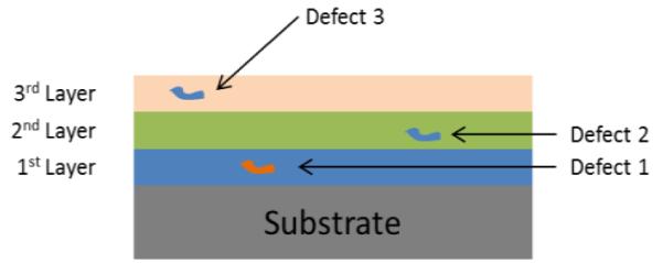
Schematic of how multiple layers can overlap defects on individual layers to decrease the probability of failure.
II. Phase 1
In the first phase of this investigation, we studied the lifetime of polymer-coated interdigitated electrodes (IDEs) fabricated on printed circuit boards (PCBs) exposed to saline at 40°C. Figure 2 shows a schematic representation of the two test specimen designs included in this investigation. The inter-electrode resistance was measured periodically upon exposure. The initial resistance values were greater than 109 Ω and failure was declared when the resistance dropped to 108 Ω. The coatings were applied using a brush or roller. Initial samples were encapsulated with a single layer of PDMS. These structures had a lifetime ranging from several hours to 6 days. Based on these results, all subsequent samples were coated with at least 3 distinct. Each layer was roller cast and a curing step was performed between each layer. The nominal thickness of each layer was estimated to be roughly 100 μm. For the multilayer studies, several polymeric films were tested, including Hysol epoxy and Medical grade PDMS (Dow Corning MDX-4 4210). The hysol epoxy and medical grade PDMS exhibited the longest lifetimes of all materials in 40°C saline, with maximum value ranging from 30 to 40 days for a single material coating. The failure spots were small and difficult to locate even under a microscope. We found that by applying a potential of 10V across the IDEs on a failed device, a small current would flow and after many hours the copper electrodes would become blue, indicating that Cu(OH)2 had deposited at the failure spot as a result of moisture-induced oxidation.. Through optical inspection, we found that failures were associated with: 1) small air bubbles in the polymer layers, 2) foreign particles (dusts and fibers), 3) sharp spikes due to solder connections, 4) vertical steps in the substrate and other structures with a very small radius of curvature, and 5) ionic contamination of the substrate surface. To address issues related to particulate and ionic contamination, a substrate cleaning process was incorporated in subsequent coating processes and the coatings were applied in a particulate controlled environment [8]. A second set of experiments using 15 PCBs were made, each coated with PDMS and tested in saline at 40°C. Three of the devices had an average coating thickness of 254 μm and exhibited a life time of ~ 35 days. Eight of the test structures were protected with a 175 μm-thick PDMS coating and had an average lifetime of 32 days. The maximum life time of the eight 175 μm-thick PDMS coated devices was 53 days, and 93 days for a 246 μm thick FP4450 epoxy coated device [9].
Fig. 2.
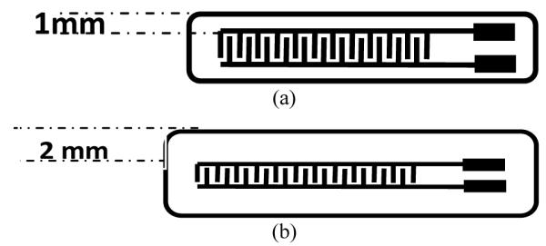
PCB Test Board structure (a) with a narrow edge, (b) with a wide edge.
The same processes were used to package several 2-channel micropower telemetry units. Each unit was packaged with two layers of different materials (FP4450 + PDMS) with total thickness of about 250 μm. Two of these units were evaluated in saline at 40°C. The #10 telemetry unit had a lifetime of 73 days. In this case, failure was defined when the current consumption of the device increased from its initial value of 0.610 μa to 0.657 μa, an 8% increase. Figure 4 shows the consumed current versus time for this device [8, 9]. After reaching the failure point, the device was retrieved from solution, cleaned and dried. Upon retesting, the device returned to its original operating status with respect to consumed current. Interestingly, this result shows that the lifetime of the packaged telemetry unit is smaller than but almost equal to the sum of the lifetimes of the two materials that constitute the multilayered package (FP4450 + PDMS).
Fig. 4.
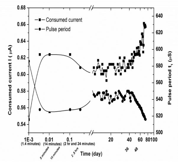
Consumed power versus time for the packaged telemetry device shown in Fig. 3.
III. PHASE 2
In order to improve the lifetime of PDMS packaging and to decrease the overall thickness of the encapsulant, a second phase of this investigation was recently. A principal objective of Phase 2 was to investigate the efficacy of multilayer approach for encapsulants that consist only of PDMS and have an overall thickness less than 100 μm [10]. Such encapsulants would be advantageous for mechanically flexible microsystems (such as neural interfaces) where mechanical compliance and low form factor are highly desired.
In this phase of the investigation, eight test coupons containing eight IDEs fabricated on PC boards were first subjected to a multi-step ultrasonic cleaning procedure. Samples were coated using Dow Corning MDX4-4210 Biomedical Grade Elastomer by roller casting immediately after the cleaning and/or surface treatment. Each IDE received 100 roller strokes at a rate of 1.5 strokes/s and a force equivalent of 250 to 300 g. Samples were cured under vacuum at 70°C. The roller casting process was repeated twice more with a curing step performed between each process. The third coating was cured for 16 hours. Film thicknesses ranged from 40 to 70 μm.
A data acquisition system was designed and constructed to continuously monitor the leakage current of the samples soaked in saline at both 40°C and 85°C. The system was designed to determine average surface insulation resistance as a function of time by monitoring the leakage current between the adjacent electrodes. Typically the IDE’s exhibited surface insulation resistance in the 10 GΩ range prior to emersion in the saline bath. Failure of the encapsulant was defined when the average surface insulation resistance dropped below 100 MΩ.
Samples were evaluated using conventional accelerated lifetime testing [11-12]. Leakage current was continuously monitored for 32 samples soaked in saline at 40°C and 32 samples soaked at 85°C. Fig. 5 shows the surface insulation resistance vs. time for a representative sample while Table 1 summarizes the results at 85°C. The maximum lifetime of samples subjected to testing at 85°C was 42 days.
Fig. 5.
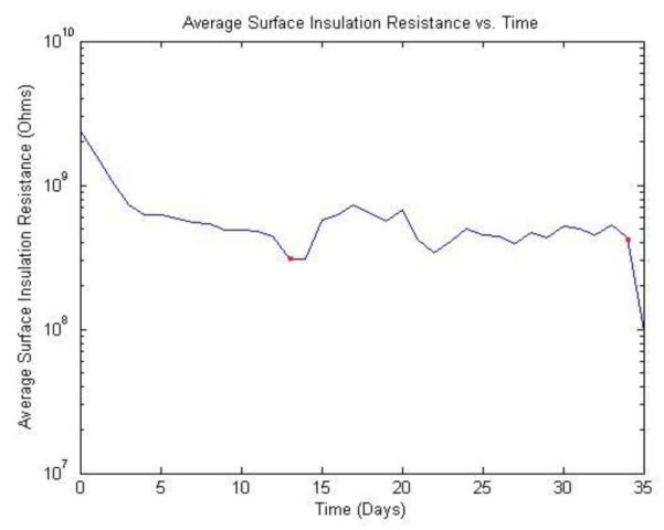
Average surface insulation resistance vs. time for a sample subjected to accelerated lifetime testing at 85°C in saline. This particular encapsulant failed after 35 days of testing.
TABLE 1.
RESULTS OF ACCELERATED LIFETIME STUDY AT 85°C.
| Days of field usage |
Number of failed plasma treated devices |
Number of failed untreated devices |
|---|---|---|
| 10 | 8 | 11 |
| 20 | 13 | 9 |
| 30 | 0 | 4 |
| 40 | 1 | 3 |
| 50 | 1 | 5 |
After failure, samples exposed to accelerated lifetime tests at 85°C were examined for evidence of coating failure. Fig. 6 is a photograph of a test coupon after electrical failure. The photograph shows that for this sample, electrical failure is associated with voids that formed between the PDMS coating and the PCB substrate. It is likely that these voids are a result of hydrogen gas formation caused by electrolysis of moisture that penetrated the coating.
Fig. 6.
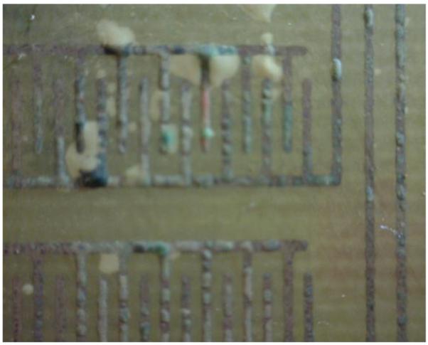
Optical photograph of an IDE after testing at 85°C showing a defect that led to device failure.
Fig. 7 shows surface insulation resistance versus time from one of the 32 samples subjected to the 40°C soak tests. No failures have been observed for any samples in this testing group after 228 days. To the best of our knowledge, this represents the longest successful accelerated lifetime test for PDMS-based packages, especially in sub 100 μm thickness range. Using an activation energy of 0.79eV calculated using an acceleration ratio of 38.8 [9], the estimated lifetime of the roller-cast PDMS encapsulant is 5.5 years at physiological temperature.
Fig. 7.
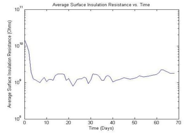
Average surface insulation resistance vs. time for a sample subjected to accelerated lifetime testing at 40°C in saline. This sample is still under test after 228 days.
IV. Conclusion
The multilayer technique has shown to be an excellent encapsulating technique for packaging implantable micro-electromechanical systems. Accelerated lifetime tests in saline at 85°C indicate that a PDMS-based trilayer has potential for use in long-term implant applications, an observation that is supported by tests at 40°C in saline. At the very least, the multilayer approach appears to be suitable for packaging microdevices for fundamental medical research. The simplicity and lower cost and time make the evaluation of non-hermetic packaging of implant systems a worthy subject for further study.
Fig. 3.
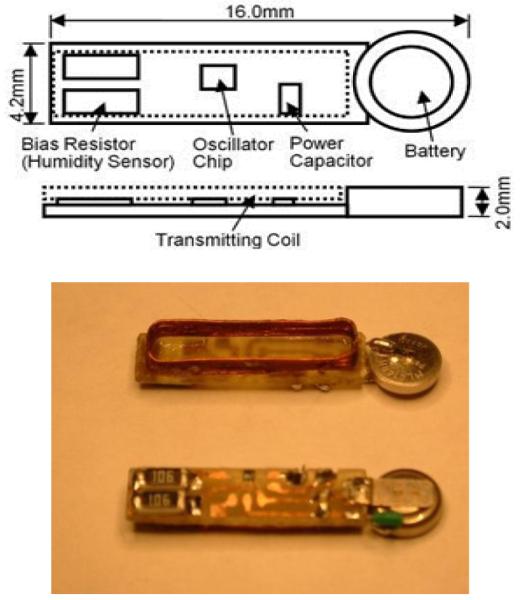
(top) Schematic diagram of the telemetry unit used to evaluate the PDMS-based package developed in Phase 1 [8], and (bottom) photograph of telemetry unit.
Acknowledgment
The authors acknowledge the research support of NIBIB, NIH and thank the management and staff of the Advanced Platform Technology Center of Excellence at the Louis Stokes VA Medical Center, Cleveland Ohio for financial and technical assistance.
Footnotes
Research supported by the Advanced Platform Technology Center, Louis Stokes VA Medical Center, Department of Veterans Affairs, Cleveland Ohio, USA, and NIBIB, of NIH.
Contributor Information
S. Lachhman, Department of Electrical Engineering and Computer Science, Case Western Reserve University, Cleveland Ohio USA 44106
C.A. Zorman, Department of Electrical Engineering and Computer Science, Case Western Reserve University, Cleveland Ohio USA.
W.H. Ko, Department of Electrical Engineering and Computer Science, Case Western Reserve University, Cleveland Ohio USA (phone: 216.368.6117; fax: 216.368.6888.
References
- [1].Ko WH, Spear T. Packaging Materials and Techniques for Implantable Instruments. IEEE Eng. Med. And Biol. Magazine. 1983 Mar;2:22–38. 1983. [Google Scholar]
- [2].Fung CD, Cheung PW, Ko WH, Fleming DG, editors. Micromachining and Micropackaging of Transducers, Elsevier, Armsterdam. 1985. [Google Scholar]
- [3].Ko WH, Neuman MR, Lin KY. Body Reaction of Implant Packaging Materials. In: Stuart L, editor. Biomaterials. Vol. 10. Plenum Press; New York: 1969. pp. 55–65. [Google Scholar]
- [4].Ko WH. Materials Chemistry and Physics. Vol. 42. Elsevier; 1995. Packaging of Microfabricated Devices and Systems; pp. 169–175. [Google Scholar]
- [5].Asano A, Takegoshi K. Free volume study of amorphous polymers detected by solid-state 13C NMR linewidth experiments. J. Chem. Phys. 2001;115:8665. [Google Scholar]
- [6].Bronshtein ÉÉ, Va BS. Probability method of assessing the quality of multilayer coatings. Chemical and Petroleum Engineering. 1989;25(1):42–45. [Google Scholar]
- [7].Golovin VA. Multilayer Protective Polymeric Coatings:Providing for Their Continuity. Protection of Metals. 2007;43(7):679–688. [Google Scholar]
- [8].Bu L, Cong P, Kuo H, Yeh X, Ko W. Micro-package of Short Term Wireless Implantable Microfabricated Systems. IEEE EMBS, EMBC; Ann. Int. Conf. Proc., Paper SaET7.4; 2009. pp. 6395–6399. (2009). [DOI] [PubMed] [Google Scholar]
- [9].Zhang R. M.S. Thesis. Case Western Reserve University; Cleveland, OH: 2011. The Study of MEMS Acoustic Sensor for Totally Implantable Hearing-Aid System and Micropackage Technology for Implantable Devices. [Google Scholar]
- [10].Lachhman SB. M.S. Thesis. Case Western Reserve University; Cleveland, OH: 2012. Evaluation and accelerated lifetime studies of Medical grade poly-dimethylsiloxane as an encapsulation material for totally implantable Wireless microelectromechanical systems. [Google Scholar]
- [11].Ulrich RK, Brown WD. Advanced Electronic Packaging: 2nd Edition. Wiley-IEEE Press; 2006. [Google Scholar]
- [12].Zhang R. M.S. Thesis. Case Western Reserve University; Cleveland, OH: Aug, 2011. [Google Scholar]


