

Abstract
Fluorescent nanodiamonds were produced by incorporation of silicon-vacancy (Si-V) defect centers in as-received diamonds of averaged size ∼255 nm using microwave plasma chemical vapor deposition. The potential for further enhancement of Si-V emission in nanodiamonds (NDs) is demonstrated through controlled nitrogen doping by adding varying amounts of N2 in a H2 + CH4 feedgas mixture. Nitrogen doping promoted strong narrow-band (FWHM ∼ 10 nm) emission from the Si-V defects in NDs, as confirmed by room temperature photoluminescence. At low levels, isolated substitutional nitrogen in {100} growth sectors is believed to act as a donor to increase the population of optically active (Si-V)− at the expense of optically inactive Si-V defects, thus increasing the observed luminescence from this center. At higher levels, clustered nitrogen leads to deterioration of diamond quality with twinning and increased surface roughness primarily on {111} faces, leading to a quenching of the Si-V luminescence. Enhancement of the Si-V defect through controlled nitrogen doping offers a viable alternative to nitrogen-vacancy defects in biolabeling/sensing applications involving sub-10 nm diamonds for which luminescent activity and stability are reportedly poor.
INTRODUCTION
Conventional fluorophores based on organic dyes or proteins have been extensively used in biological labeling. However, they have apparent limitations as a result of photobleaching (brightness fading) for time dependent studies of in vitro or in vivo processes. Their emission spectra often overlap with the emission (400–550 nm) of inherent endogenous components such as flavin and nicotinamide as well as with the diamond background emission.1 Semiconductor nanocrystals “quantum dots” (QD) have much higher photobleaching thresholds. However, surface modifications are often necessary to reduce toxicity and to increase water solubility2 which inevitably changes their photophysical properties.3, 4 In addition, QDs suffer from intermittency in their emission, called “blinking.” Nanodiamond (ND) particles offer an emergent technology with one of its main applications as a perfectly photostable luminescent emitter upon incorporation of color centers, such as the predominantly studied negatively charged nitrogen-vacancy (NV) defect.5, 6 The majority of studies on ND have revealed low cytotoxicity7 and low animal toxicity,8 and have demonstrated that the surface can be easily modified with a wide range of functional groups to provide a versatile platform for conjugation with small molecules, proteins, and nucleic acids.9 These properties have led to intense interest in ND not only as an imaging probe but also as a drug and gene delivery platform. The room temperature fluorescence spectrum of NV centers has broad phonon side band (∼100 nm) due to the strong electron phonon coupling that may hamper spectral distinction between the color center fluorescence and background signals.10 Additionally, due to the zero phonon line (ZPL) for NV− at 638 nm, excitation with visible laser light (typically 532 nm) is necessary and this leads to auto fluorescence of biological tissues.11 Density functional tight binding simulations predict the preferable positioning of nitrogen as being at the surface of NDs, where formation of NV defects is unlikely to occur.12 The ability to produce and detect NV centers in isolated sub −10 nm NDs is strongly debated, and skepticism remains as to their stability as a useful emitter in a discrete NDs smaller than 10 nm.13 Very recently, NV centers in discrete 5 nm ND were reported, although luminescence blinking was observed.5 Moreover, emission from both the charge states of NV (i.e., ∼575 nm and ∼638 nm for NV0 and NV−, respectively) is weak and often difficult to distinguish from the broad ND background fluorescence. Therefore, the silicon vacancy (Si-V) color center has emerged as an alternative emitter because of its numerous promising properties including: sharp zero phonon line (with full width at half maximum (FWHM) ranging from 0.7 to −10 nm) at 738 nm, short fluorescence lifetime of about 2 ns (compared to 13 ns for NV center), and spectral distinction from the characteristic broad band photoluminescence (PL) of ND (spread between 450 nm and 650 nm).14, 15, 16 Since the silicon atom enters the diamond lattice interstitially and sits in the center of a split vacancy, this center does not couple strongly with the diamond phonons (in contrast to NV center). The result is a relatively narrow fluorescence spectrum with a sharp ZPL, and a relatively weak phonon side band.15 Thus, the Si-V defect becomes a promising candidate for efficient single photon source, but it also has great potential as biolabel/drug delivery agent that has not yet been realized. Si-V has been investigated mainly in the form of thin chemical vapor deposited (CVD) films with less consideration in the form of isolated nanocrystals which are particularly relevant as biolabels or as a drug-delivery platform.17 Unfortunately, initial reports suggested relatively low brightness of the Si-V center in diamond as a result of a poor quantum efficiency due to a very high non-radiative decay term, limiting its quantum efficiency to only 5%.18 In this paper, we report that controlled nitrogen doping of diamond nanocrystals leads to an increased emission intensity of the Si-V defect center, with an associated evolution in diamond morphology and quality. The emission enhancement is described in terms of the expected influence of nitrogen on the energy of the defects in the diamond bandgap.
EXPERIMENTAL DETAILS
Microwave plasma chemical vapor deposition (MPCVD) was used with a range of nitrogen feedgas addition (0.04–0.115 vol. %) to incorporate Si-V color centers in NDs. Si-V defect centers were created in ND particles seeded onto ∼6 × 6 mm2 silicon (100) substrates. Synthetic high-temperature/high-pressure diamond milled to an average particle size of ∼255 nm (Engis Corp.) was used as raw material. The as-received NDs were dispersed in de-ionized water (concentration 0.05% w/v) and ultrasonicated 60 min to serve as a seeding solution for silicon substrates. Dynamic light scattering measurements (Zetasizer Nano ZS; Malvern Instruments, Ltd) of NDs dispersed in de-ionized water confirmed a left-skewed size distribution with peak at 283 nm having a band width 22 nm (i.e., 283 ± 44 nm) but the mean of this size distribution is at ∼255 nm. The silicon substrates were ultrasonically cleaned in acetone for 10 min before seeding. The suspension was then pipetted (∼10 μl) onto Si wafer and allowed to dry, followed by removal of loose particles by blowing dry nitrogen. The seeded substrates were exposed to a MPCVD process for 30 min using 14 sccm methane in a hydrogen rich feedgas mixture (0.7% CH4 with respect to the total flow of 2000 sccm), 800–820 °C substrate temperature, 45 Torr chamber pressure, and 900 W microwave power. Incorporation of Si-V defects occurs as a result of plasma chemical etching of the exposed Si substrate in the hydrogen-rich plasma. The etched silicon species are re-deposited with diamond to form the defect center. Nitrogen doping was achieved by adding nitrogen (N2) with a flow rate of 0.8–2.3 sccm (flow accuracy ±0.1%) to the fixed H2 + CH4 CVD feedgas mixture in order to keep the total flow constant at 2000 sccm). The nitrogen concentration is reported as a percentage of the total flow, ranging from 0.04% to 0.115%.
In this paper, we report the dramatic influence that nitrogen doping has on room temperature photoluminescence from the Si-V defect center and relate this to observed changes in particle morphology and crystal quality. In order to confirm the presence of Si-V and NV defects, room temperature PL spectroscopy (excitation wavelength of 532 nm) was performed on pre- and post-CVD NDs on the silicon substrates, respectively. Micro-Raman spectroscopy (532 nm excitation) Nd:YAG solid state laser source was used to determine the diamond crystal quality. Atomic force microscopy (DPN5000, Nanoink, Inc.) was used to estimate the size of the diamond crystals as well as the roughness of {111} and {100} faces of individual diamond crystals. Scanning electron microscopy (SEM) was used to observe the distribution of ND crystals on the silicon substrate.
RESULTS
The distribution of diamond nanocrystals on the silicon substrate for pre- and post-CVD (undoped, with 0.04% N2 in feedgas, and with 0.115% N2 in feedgas) is shown in the SEM images of Fig. 1. The majority of the surface is covered with clusters of ND crystals, although some isolated crystals could be found for further analysis. We observed that the ND crystals changed dramatically from being irregularly shaped (pre-CVD) to predominantly cubo-octahedral (post-CVD undoped and N2-doped). The ND crystals consist primarily of randomly oriented {111} and {100} faces. The crystal size increased from ∼600 nm for undoped to ∼1 μm for 0.115% N2-doped NDs. The increase in the size of the crystallites indicates increased growth rate due to the catalytic influence of nitrogen on the surface.19 AFM images of the undoped and N2-doped NDs are shown in Fig. 2 with four different isolated particles shown for each N2 doping level. The undoped diamond crystals have cubo-octahedral shape consisting of smooth well-defined {100} and {111} faces without much evidence of growth steps, secondary nucleation, or micro-twinning. As shown in previous studies, nitrogen is preferentially incorporated into {111} faces by a factor of three to four compared to {100} faces.20 At very low N2 concentrations (0.04%), both {100} and {111} faces begin to show surface roughening, and this roughening increases with higher N2 concentrations (0.115%). As shown in Fig. 3, ND crystals doped with increasing N2 have {111} faces with increased roughness compared to the {100} face, presumably due to multiple twinning.21, 22 For the highest nitrogen doping concentration of 0.115%, {111} faces exhibit substantial surface roughening and {100} faces begin to exhibit growth steps. The increasing nitrogen concentration leads to a loss of faceting and a reduction of diamond phase purity. This becomes evident from the intensity reduction and broadening of the diamond Raman spectroscopy peak (ca. 1332 cm−1), as shown in Fig. 4. All Raman spectra in Fig. 4 except for the pre-CVD (raw) spectrum exhibit a broad band between 1400 and 1600 cm−1 attributed to non-diamond carbon phase. With increasing nitrogen feedgas addition from 0% to 0.115% N2, the FWHM of the crystalline sp3-diamond Raman peak at 1332 cm−1 increases. Fig. 5 shows the variation of the 1332 cm−1 diamond Raman peak integrated intensity as well as its FWHM as a function of nitrogen concentration. The intensity reduction and broadening of the 1332 cm−1 peak as the N2 concentration increases up to 0.065% indicate deterioration of diamond quality. Beyond this, higher nitrogen concentrations did not result in a significant change in the 1332 cm−1 peak intensity. Room temperature PL spectra (excitation 532 nm) of pre- and post-CVD (undoped and N2-doped) NDs are shown in Fig. 6, for which the pre-CVD average ND size was ∼255 nm. The PL spectra show band emission ca. 738 nm, characteristic of the zero phonon line of the Si-V defect center for both undoped and N2-doped diamonds. For undoped diamonds, a rather weak but sharp (FWHM ∼ 7 nm) zero phonon line lies on the background fluorescence. The FWHM increased to ∼11–12 nm for 0.04%–0.115% N2-doped NDs. The integrated intensity of Si-V center as a function of N2 concentration is shown in Fig. 7. A maximum in Si-V emission is observed for a nitrogen feedgas concentration of 0.04%. A similar dependence of Si-V intensity with N2 concentration has been reported elsewhere, but with no clear evidence or explanation to support the trend.23 We also observed the same trend for Si-V emission as a function of N2 concentration as shown in Figs. 67 by exciting 4 × 4 mm2 areas of pre-CVD and post-CVD samples with 494 nm xenon excitation light using Horiba Flurolog-3 spectrofluorometer (see supplementary data31). This eliminates the possibility that the observed trend is somehow dependent on the number of NDs per unit area. It should be noted that the pre-CVD NDs exhibit a 638 nm zero phonon line associated with the NV− center indicating that the raw diamond inherently has nitrogen defects. However, there was no emission from Si-V in the raw pre-CVD NDs.
Figure 1.

SEM images of (a) pre-CVD, (b) undoped, (c) nitrogen doped with N2 = 0.04%, and (d) nitrogen doped with N2 = 0.115% ND particles. Surface roughening, primarily on {111} faces, increases with nitrogen doping. The presence of non-diamond carbon phase is a result of the deterioration of the crystallites, especially {111} faces by the nitrogen-induced micro-twinning on its surface,21, 30 eventually leading to a highly twinned nanocrystalline appearance. The 2 μm scale bar is the same for each image.
Figure 2.

AFM images of four isolated nanodiamond particles for each nitrogen feedgas concentration (0%, 0.04%, and 0.115%). Deterioration/roughening is enhanced on {111} faces with increasing N2 feedgas concentration. Each scale bar corresponds to 0.2 μm.
Figure 3.
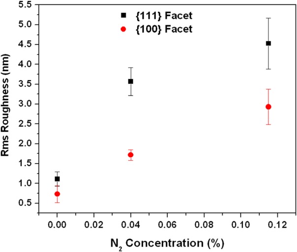
RMS roughness of the {111} and {100} facets with various nitrogen flows, averaged over 4 particles for each N2 concentration.
Figure 4.
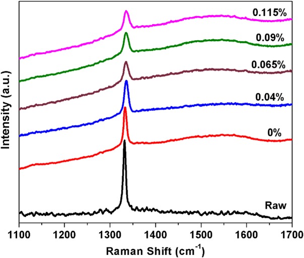
Normalized Raman spectra of ∼255 nm as-received (pre-CVD), undoped and nitrogen doped NDs.
Figure 5.
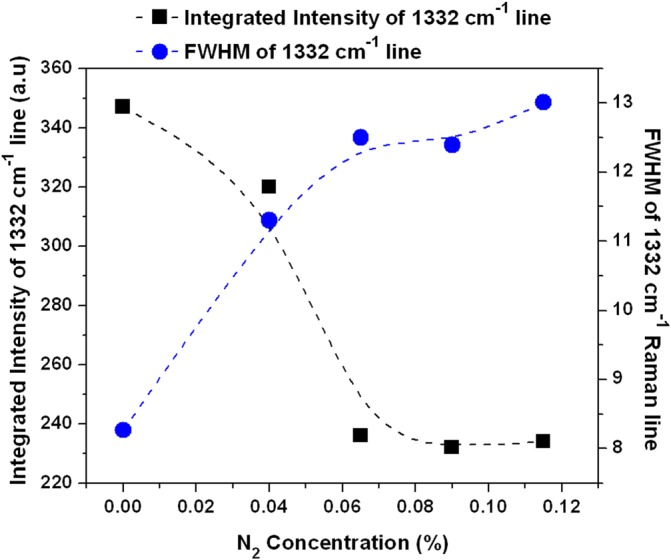
Integrated intensity and FWHM of 1332 cm−1 Raman line as a function of N2 concentration.
Figure 6.
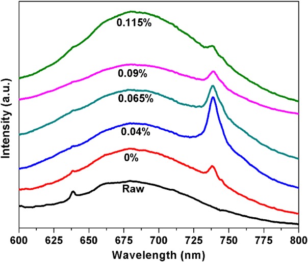
The room temperature photoluminescence (excitation 532 nm) of nanodiamonds with varying nitrogen flow 0%-0.115% in hydrogen feedgas, along with as-received (pre-CVD) nanodiamonds. An increased amount of nitrogen enhances the intensity from Si-V color centers up to a maximum nitrogen flow of 0.04%. The average size of as-received ND is 255 nm.
Figure 7.

Variation of room temperature integrated photoluminescence intensity of Si-V zero phonon line at ∼738 nm with nitrogen concentration in NDs. Error bars represent the standard deviation from 3 experiments. The average size of as-received ND is 255 nm.
DISCUSSION
As mentioned earlier, there are several promising aspects of Si-V color centers ranging from their use as a single-photon source to a luminescent biolabel. However, initial reports of low brightness of the Si-V centers in diamond revealed a poor quantum yield.18 The local atomic environment around a Si-V center is expected to influence photon emission characteristics, especially if it results in substantial non-radiative transitions. Si-V centers have non-radiative charge states such as (Si-V)0/(Si-V:H)0/(Si-V2) as shown in Fig. 8, and in the case of natural semiconducting diamond with negligible nitrogen content, the luminescence of Si-V centers was not detectable.24 However, by manipulating the occupancy of the charge states with a high concentration of isolated nitrogen, photoluminescence of Si-V centers ∼738 nm may be relatively more intense.
Figure 8.

Schematic showing the position of optically active and inactive charge states for Si-V center in the diamond band gap.
We suggest a model such that nitrogen incorporation in diamond, especially within {100} growth sectors, is related to the observed enhanced emission from Si-V defects. The population of optically active Si-V centers is low in undoped diamonds, resulting in the observed weak luminescence. In undoped and very low level N2-doped ND, both {100} and {111} faces in the cubo-octahedral crystals are evident with low roughness and improved quality compared to the case of diamond grown with higher N2 concentrations (>0.065%). Nitrogen is preferentially incorporated into {111} growth sectors. For very low N2 concentration (up to 0.04% in this study), it is expected that isolated substitutional nitrogen atoms in the {100} face act as donors in diamond and raise the Fermi-level to a position near the conduction band, charging the Si-V defects negatively.25 Although our results do not provide direct experimental evidence for the substitutional nature of nitrogen incorporation on {100} faces, substitutionally incorporated nitrogen in {100} faces has been reported using electron paramagnetic resonance for homoepitaxial diamond films grown by MPCVD.26 It has also been shown to occur in highly oriented {100} textured polycrystalline CVD diamond films as well as in randomly oriented crystallites.27 The resulting charged (Si-V)− centers are optically active and contribute to the luminescence. Therefore, the population of optically active (Si-V)− centers increases at the expense of optically inactive Si-V centers. With higher position of the Fermi-level, the fraction of Si-V centers in the optically inactive charge state becomes smaller and the effect of correlated emission is reduced. As a result, the emission of Si-V centers increases.
An optically inactive charge state can provide a channel for non-radiative transitions. The Si-V center has a ground state energy at Ec − 2.05 eV, which results in an excited state close to the conduction band, making photothermal ionization possible. If the Si-V center loses an electron, it becomes positively charged and is incapable of photon emission. The positively charged state has energy Ev + 2.5 eV and can be regarded as the “shelving level” in a three-level model. The schematic representation of the position of non-radiative (Si-V)0/(Si-V:H)0/(Si-V2) and optically active (Si-V)− charge states for Si-V center in the diamond band gap is given in Fig. 8. At low levels, nitrogen will reside in {111} growth sectors and C-N bond will become longer than the C-C bond, leading to a distortion on the {111} face.28 Therefore, the {111} face deteriorates with a corresponding increase in roughness while growth proceeds along the {100} face resulting in growth steps on its surface. For large N2 concentrations (>0.04%), nitrogen will begin to accumulate within {100} growth sectors in cluster form rather than as isolated substitutional form. This excessive nitrogen is known to deteriorate the phase purity of diamond leading to increased sp2-bonded carbon. Clustered nitrogen in {100} face may also produce changes in bonding and structure of diamond to form other defects such as N2 clusters along with Si-V defects. The decrease of Si-V intensity with increasing nitrogen (beyond 0.04%) can be attributed to the quenching of the Si-V luminescence signal as a result of this N2 clustering as well as to the presence of non-diamond carbon phases.29 The broadening of 1332 cm−1 Raman peak as shown in Fig. 5 also indicates that diamonds have very high density of defects and non-diamond carbon with increasing N2 concentration.
The potential for enhanced Si-V emission in sub-10 nm size diamond crystals exists, and studies suggest that it may be more favorable to occur than for N-V incorporation in similar size crystals. For example, density functional tight-binding simulations have predicted high thermodynamic stability of Si-V centers in the ND core, which supports experimental observations of this center for the case of continuous nanocrystalline diamond films comprised of 2-5 nm grain size grown using MPCVD.15 We have also recently observed this for weakly agglomerated sub-10 nm diamond nanocrystals on silicon substrates after MPCVD diamond growth.17 Further experimental and theoretical studies are needed to establish if nitrogen doping will provide a route to enhance Si-V luminescence in discrete sub-10 nm NDs.
CONCLUSIONS
The role of controlled nitrogen doping was studied to enhance the room temperature photoluminescence emission from Si-V centers in ND crystals (∼255 nm as-received average size) on silicon substrate using MPCVD. We found that Si-V defects are efficiently incorporated into diamond crystals due to hydrogen-etching of the silicon substrate during CVD treatment. Photoluminescence spectra of post-CVD samples show a strong and narrow (FWHM of ∼10 nm) Si-V zero phonon line (ca. 738 nm) lying on a relatively weak background fluorescence. We observed a strong dependence of Si-V emission in diamond with N2 feedgas concentration. It is believed that small amounts of isolated substitutional nitrogen in {100} growth sectors acts as a donor to increase Fermi level near to conduction band and charges Si-V defects negatively. This is expected to result in the population of optically active (Si-V)− centers to increase at the expense of optically inactive Si-V defects. For higher N2 concentrations, quenching of Si-V luminescence signal is observed and may be due to the clustering of nitrogen in {100} growth sectors and associated deterioration of diamond phase purity. The significance of this work is based on the potential to efficiently incorporate and enhance Si-V luminescence in discrete diamond crystals leading to bright fluorescence through controlled doping of nitrogen, which has implications for many biological applications.
ACKNOWLEDGMENTS
The project described was supported by Award No. P30EB011319 from the National Institute of Biomedical Imaging and Bioengineering (NIBIB) as well as from (Research Core Grant), 1R01AR056665-1 1A1 (Bioengineering Research Partnership). The authors wish to thank Dr. Vinoy Thomas for his assistance with scanning electron microscopy measurements.
References
- Fu C. C., Lee H. Y., Chen K., Lim T. S., Wu H. Y., Lin P. K., Wei P. K., Tsao P. H., Chang H. C., and Fann W., Proc. Natl. Acad. Sci. U.S.A. 104, 727–732 (2007). 10.1073/pnas.0605409104 [DOI] [PMC free article] [PubMed] [Google Scholar]
- Hardman R., Environ. Health Perspect. 114, 165–172 (2006). 10.1289/ehp.8284 [DOI] [PMC free article] [PubMed] [Google Scholar]
- Michalet X., Pinaud F. F., Bentolila L. A., Tsay J. M., Doose S., Li J. J., Sundaresan G., Wu A. M., Gambhir S. S., and Weiss S., Science 307, 538–544 (2005). 10.1126/science.1104274 [DOI] [PMC free article] [PubMed] [Google Scholar]
- Kirchner C., Liedl T., Kudera S., Pellegrino T., Javier A. M., Gaub H. E., Stolzle S., Fertig N., and Parak W. J., Nano Lett. 5, 331–338 (2005). 10.1021/nl047996m [DOI] [PubMed] [Google Scholar]
- Bradac C., Gaebel T., Naidoo N., Sellars M. J., Twamley J., Brown L. J., Barnard A. S., Plakhotnik T., Zvyagin A. V., and Rabeau J. R., Nat. Nanotechnol. 5, 345–349 (2010). 10.1038/nnano.2010.56 [DOI] [PubMed] [Google Scholar]
- Bradac C., Gaebel T., Naidoo N., Rabeau J. R., and Barnard A. S., Nano Lett. 9, 3555–3564 (2009). 10.1021/nl9017379 [DOI] [PubMed] [Google Scholar]
- Faklaris O., Joshi V., Irinopoulou T., Tauc P., Sennour M., Girard H., Gesset C., Arnault J. C., Thorel A., Boudou J. P., Curmi P. A., and Treussart F., ACS Nano 3, 3955–3962 (2009). 10.1021/nn901014j [DOI] [PubMed] [Google Scholar]
- Yuan Y., Chen Y. W., Lui J. H., Wang H. F., and Liu Y. F., Diamond Relat. Mater. 18, 95–100 (2009). 10.1016/j.diamond.2008.10.031 [DOI] [Google Scholar]
- Lam R. and Ho D., Expert Opin. Drug Delivery 6, 883–895 (2009). 10.1517/17425240903156382 [DOI] [PubMed] [Google Scholar]
- Rabeau J. R., Stacey A., Rabeau A., Prawer S., Jelezko F., Mirza I., and Wrachtrup J., Nano Lett. 7, 3433–3437 (2007). 10.1021/nl0719271 [DOI] [PubMed] [Google Scholar]
- Neu E., Arend C., Gross E., Guldner F., Hepp C., Steinmetz D., Zscherpel E., Ghodbane S., Sternschulte H., Steinmuller-Nethl D., Liang Y., Krueger A., and Becher C., Appl. Phys. Lett. 98, 243107 (2011). 10.1063/1.3599608 [DOI] [Google Scholar]
- Barnard A. S., Vlasov I. I., and Ralchenko V. G., J. Mater. Chem. 19, 360–365 (2009). 10.1039/b813515k [DOI] [Google Scholar]
- Vlasov I. I., Shenderova O., Turner S., Lebedev O. I., Basov A. A., Sildos I., Rahn M., Shiryaev A. A., and Van Tendeloo G., Small 6, 687–694 (2010). 10.1002/smll.200901587 [DOI] [PubMed] [Google Scholar]
- Basov A. A., Rahn M., Pars M., Vlasov I. I., Sildos I., Bolshakov A. P., Golubev V. G., and Ralchenko V. G., Phys. Status Solidi A 206, 2009–2011 (2009). 10.1002/pssa.200982220 [DOI] [Google Scholar]
- Vlasov I. I., Barnard A. S., Ralchenko V. G., Lebedev O. I., Kanzyuba M. V., Saveliev A. V., Konov V. I., and Goovaerts E., Adv. Mater. 21, 808 (2009). 10.1002/adma.200802160 [DOI] [Google Scholar]
- Wang C. L., Kurtsiefer C., Weinfurter H., and Burchard B., J. Phys. B 39, 37–41 (2006). 10.1088/0953-4075/39/1/005 [DOI] [Google Scholar]
- Catledge S. A. and Sonal S., Adv. Sci. Lett. 4, 512–515 (2011). 10.1166/asl.2011.1264 [DOI] [PMC free article] [PubMed] [Google Scholar]
- Turukhin A. V., Liu C. H., Gorokhovsky A. A., Alfano R. R., and Phillips W., Phys. Rev. B 54, 16448–16451 (1996). 10.1103/PhysRevB.54.16448 [DOI] [PubMed] [Google Scholar]
- Dunst S., Sternschulte H., and Schreck M., Appl. Phys. Lett. 94, 224101 (2009). 10.1063/1.3143631 [DOI] [Google Scholar]
- Samlenski R., Haug C., Brenn R., Wild C., Locher R., and Koidl P., Appl. Phys. Lett. 67, 2798–2800 (1995). 10.1063/1.114788 [DOI] [Google Scholar]
- Cao G. Z., Schermer J. J., vanEnckevort W. J. P., Elst W., and Giling L. J., J. Appl. Phys. 79, 1357–1364 (1996). 10.1063/1.361033 [DOI] [Google Scholar]
- Schermer J. J., Hogenkamp J. E. M., Otter G. C. J., Janssen G., Vanenckevort W. J. P., and Giling L. J., Diamond Relat. Mater. 2, 1149–1155 (1993). 10.1016/0925-9635(93)90160-4 [DOI] [Google Scholar]
- Musale D. V., Sainkar S. R., and Kshirsagar S. T., Diamond Relat. Mater. 11, 75–86 (2002). 10.1016/S0925-9635(01)00521-0 [DOI] [Google Scholar]
- Collins A. T., Kamo M., and Sato Y., J. Mater. Res. 5, 2507–2514 (1990). 10.1557/JMR.1990.2507 [DOI] [Google Scholar]
- Yam B. and Moustakas T. D., Nature 342, 786–787 (1989). 10.1038/342786a0 [DOI] [Google Scholar]
- Yan C. S. and Vohra Y. K., Diamond Relat. Mater. 8, 2022–2031 (1999). 10.1016/S0925-9635(99)00148-X [DOI] [Google Scholar]
- Graeff C. F. O., Rohrer E., Nebel C. E., Stutzmann M., Guttler H., and Zachai R., Appl. Phys. Lett. 69, 3215–3217 (1996). 10.1063/1.117965 [DOI] [PubMed] [Google Scholar]
- Jin S. and Moustakas T. D., Appl. Phys. Lett. 65, 403–405 (1994). 10.1063/1.112315 [DOI] [Google Scholar]
- Grudinkin S. A., Feoktistov N. A., Medvedev A. V., Bogdanov K. V., Baranov A. V., Vul A. Y., and Golubev V. G., J. Phys. D: Appl. Phys. 45, 062001 (2012). 10.1088/0022-3727/45/6/062001 [DOI] [Google Scholar]
- Bohr S., Haubner R., and Lux B., Appl. Phys. Lett. 68, 1075–1077 (1996). 10.1063/1.115717 [DOI] [Google Scholar]
- See supplementary material at http://dx.doi.org/10.1063/1.4783958 for a plot showing the nitrogen-dependant SiV luminescence for large (4 × 4 mm2) irradiation areas.