Abstract
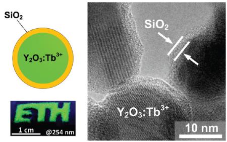
Silica-coated and uncoated, Tb-doped (1–5 at % Tb) Y2O3 green nanophosphors were made, for the first time, in a single step by flame aerosol technology with controlled crystal phase (cubic and monoclinic) and morphology. The nanophosphors were characterized by X-ray diffraction, N2 adsorption, high resolution electron microscopy, and photoluminescence spectroscopy. The monoclinic crystal structure of Y2O3:Tb3+ nanophosphors favors the electric dipole 5D4 → 7F5 transition driving their green phosphorescence. The phosphorescence of the SiO2-coated monoclinic Y2O3:Tb3+ nanophosphors is lower than the uncoated ones. Upon annealing these nanophosphors, they were transformed from monoclinic to cubic and their phosphorescence was reduced. This further indicates the superior performance of the monoclinic crystal phase for the electric dipole transitions of Tb3+ ions.
I. INTRODUCTION
Luminescent light-emitting nanoparticles have potential applications in high-definition displays,1 lasers,2 and bioimaging.3 Among these particles, rare-earth phosphors doped with lanthanide ions have advantageous optical properties for their superior photostability.4 Yttria (Y2O3) is one of the most studied ceramics as a host matrix, especially when doped with europium (Eu3+), resulting in a bright red emission.5 Furthermore, the emission color depends on the chosen dopant element.6 For example, when Y2O3 is doped with terbium (Tb3+), a bright green emission occurs.5,7 In fact, the color of nanosized Y2O3 nanocrystals can be finely tuned from bright green to red by codoping them with Tb3+ and Eu3+ during their flame synthesis without altering their crystal and particle sizes by such doping.8
Such nanocrystals are particularly attractive for bioimaging, as they do not degrade during analysis (photobleaching) compared to organic dyes and are relatively nontoxic compared to semiconducting (e.g., CdSe, PbS) nanoparticles (quantum dots).3,9 For such bioapplications, the nanoparticle surface often needs to be modified to increase its biocompatibility. Recently, it was shown that a dense nanothin silica layer10,11 drastically minimized the toxicity of plasmonic nanosilver, as it prevented the release of toxic ions and the direct contact of nanosilver with human cells.12 In fact, such a layer can facilitate surface biofunctionalization for specific molecule binding10 and the dispersion of nanophosphors.11
The crystal structure and particle size of the host matrix (e.g., Y2O3) can influence the luminescent properties of nanophosphors.13 For example, the luminescence of monoclinic Y2O3 doped with Eu3+ is lower than that of cubic Y2O3, so the luminescence of the latter has been studied extensively.13-16 Monoclinic Y2O3 can be made efficiently also, especially at high temperatures and fast cooling rates.13,17 In cubic Y2O3, there are two sites where rare earth ions can substitute Y3+: one with C2 symmetry and without any inversion center (75% of the sites) and one with S6 symmetry with an inversion center.18,19 In monoclinic Y2O3, all sites have Cs symmetry without any inversion center.19 It has been shown theoretically as early as in 1967 that for green luminescence Tb3+ ions should be embedded in lattice sites without inversion symmetry, such as the monoclinic Y2O3.20 Nevertheless, as the red emission of monoclinic Y2O3:Eu3+ is less intense than that of its cubic phase,13 a few have investigated the luminescence of monoclinic Y2O3:Eu3+ nanoparticles13,17,21,22 and even fewer have involved other lanthanides such as Tb3+.19,22,23
Here, silica-coated and uncoated Y2O3:Tb3+ nanophosphors are made by flame aerosol technology with controlled size and crystal phase (cubic and monoclinic). Flame synthesis is attractive, as it typically yields high-purity crystalline nanoparticles.13 The Tb-content ranges from 1 to 5 at %. The nanophosphors are characterized by X-ray diffraction, N2 adsorption, and high-resolution electron microscopy and their optical properties by photoluminescence spectroscopy. The effect of Y2O3 crystallinity and silica coating on the luminescence of Y2O3:Tb3+ nanophosphors is investigated. The monoclinic Y2O3 nanophosphors are annealed up to 1100 °C for 10 h to monitor the influence of the resulting phase transition from monoclinic to cubic on their phosphorescence.
II. EXPERIMENTAL SECTION
SiO2-coated monoclinic Y2O3:Tb3+ nanophosphors were made in an enclosed flame-spray reactor.24 In brief, yttrium nitrate (Aldrich, 99.9%) was dissolved in a 1:1 by volume mixture of 2-ethylhexanoic acid (EHA, Riedel-de Haen, 99%) and ethanol (Alcosuisse) to form the precursor solution. Its molarity was kept constant at 0.5 M for Y metal. The Tb doping was achieved by adding 1–5 at % Tb nitrate (Aldrich, 99.9%) to the above solution. The Tb atomic fraction (at %) was defined with respect to the total metal ion concentration. The precursor solution was fed to the spray nozzle (5 mL/min) and dispersed by 5 L/min oxygen (PanGas, purity >99.9%) and sheathed by 40 L/min oxygen. The freshly formed core Y2O3:Tb3+ particles were coated in-flight by swirl injection of hexamethyldisiloxane (HMDSO, Sigma Aldrich, purity ≥99%) vapor with 15 L/min nitrogen (PanGas, purity >99.9%) at room temperature through a metallic ring with 16 equidistant openings. The ring was placed on top of a 20 cm long quartz glass tube (inner diameter 4.5 cm) based at the spray nozzle followed by another 30 cm long such tube.24 The HMDSO vapor was supplied by bubbling 0.5 L/min N2 at 9 °C through approximately 350 mL of liquid HMDSO in a 500 mL glass flask.24 The SiO2 fraction in the product particles was kept at 16.6 wt %, assuming HMDSO fed at saturation conditions.24 The as-prepared nanophosphor particles were collected on a glass microfiber filter (Whatman GF6, 257 mm diameter). Uncoated monoclinic Y2O3:Tb3+ particles were made under identical conditions as the above, in the absence, however, of HMDSO vapor. Uncoated cubic Y2O3:Tb3+ nanophosphors were made8 by feeding 11.6 mL/min of the precursor solution to the spray nozzle and dispersed to a fine spray by 3 L/min oxygen without any enclosure.
X-ray diffraction (XRD) patterns were recorded by a Bruker AXS D8 Advance diffractometer (40 kV, 40 mA, Cu Kα radiation) at 2θ = 20–70° with a step size of 0.03°. The obtained spectra were fitted using the TOPAS 3 software (Bruker) and the Rietveld fundamental parameter refinement.13 High resolution transmission electron microscopy (HR-TEM) was performed with a CM30ST microscope (FEI; LaB6 cathode, operated at 300 kV, point resolution ~2 Å). Product particles were dispersed in ethanol and deposited onto a perforated carbon foil supported on a copper grid. Their photoluminescence was characterized at room temperature using a fluorescence spectrophotometer (Varian Cary Eclipse) containing a Xe flash lamp with tunable emission wavelength. Samples of 30 ± 2 mg were filled in a cylindrical substrate holder of 10 mm diameter and pressed toward a quartz glass front window. Emission spectra were recorded at 450–650 nm and excitation spectra at 200–400 nm with a step size of 0.5 nm. The decay time of the luminescence emission was determined by time-resolved measurements of the luminescence intensity with a resolution of 0.11 ms. Software supplied by Varian fitted exponential decay curves into the measured data points. Annealing of the samples was performed at 750, 850, 900, and 1100 °C for 10 h in an oven (Carbolite, CWF 1300) in air at ambient pressure.
III. RESULTS AND DISCUSSION
Morphology and Crystallinity of Y2O3:Tb3+ Nanoparticles
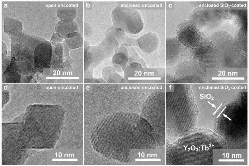
Figure 1 shows HR-TEM images at two magnifications of uncoated Y2O3:Tb3+ (2 at % Tb) nanoparticles made by open (a, d) and enclosed (b, e) spray flames, in which the crystal planes of the Y2O3 matrix can be seen.8 For the uncoated Y2O3 from the open flame (a, d), there are both spherical and rhomdohedrally shaped particles,13 while, for the Y2O3 made by the enclosed flame (b, e), there are mostly spherical. For the SiO2-coated nanoparticles made by the enclosed flame (c, f), a smooth amorphous SiO2 layer of about 2 nm encapsulates the crystal core, as with SiO2-coated TiO2,24 Fe2O3,25 and Ag11 nanoparticles.
Figure 1.
High-resolution transmission electron microscopy images from the open uncoated (a, d), enclosed uncoated (b, e), and enclosed SiO2-coated (c, d) Y2O3:Tb3+ (2 at %).
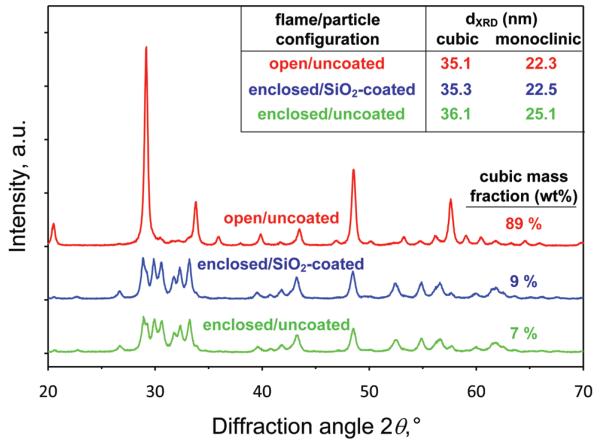
Figure 2 shows the XRD spectra of the Y2O3:Tb3+ (2 at %) nanoparticles of Figure 1. The ones made in open flames are mostly cubic (89%), in agreement with the literature8,26 at these conditions (11.6 mL/min precursor solution feed rate, 3 L/min dispersion gas flow rate). The Y2O3 nanoparticles made by the enclosed flame, however, have only a minimal cubic fraction (<10%) and exhibit the characteristic pattern of the monoclinic phase.27 Additionally, the presence of the SiO2 coating does not significantly influence nanoparticle crystallinity,25 as the XRD patterns of uncoated and SiO2-coated nanoparticles are almost identical. The average crystal sizes (Figure 2, inset) of nanoparticles made by open (from now on, cubic Y2O3) and enclosed flame (from now on, monoclinic Y2O3) are similar for all three conditions, which facilitates their further luminescent evaluation, as shown later on.
Figure 2.
X-ray diffraction patterns of open uncoated, enclosed uncoated, and enclosed SiO2-coated Y2O3:Tb3+ (2 at %). The open FSP made Y2O3:Tb3+ nanoparticles exhibit the characteristic cubic crystal structure, while both enclosed FSP made nanoparticles exhibit the monoclinic Y2O3 crystal structure. The average crystal sizes of the cubic and monoclinic phases and the corresponding mass fraction of the cubic phase are also shown.
Phosphorescence of Cubic and Monoclinic Y2O3:Tb3+ Nanoparticles
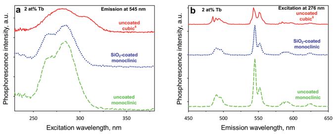
Figure 3a shows the excitation spectra of uncoated cubic8 (solid line), uncoated monoclinic (broken line), and SiO2-coated monoclinic (dotted line) Y2O3:Tb3+ (2 at % Tb) nanoparticles monitoring their emission at 545 nm. The cubic Y2O3:Tb3+ nanoparticles have a dominant band centered around 280 nm and a secondary band centered around 310 nm.5,9,28 The monoclinic Y2O3:Tb3+ have the dominant band centered also around 280 nm but the secondary excitation band around 265 nm. These bands are assigned for the Tb3+ transitions within the phosphor particles.28 This is the first indication that the crystal phase of the Y2O3 host matrix influences the luminescent properties.
Figure 3.
(a) The excitation spectra of the 2 at % Tb-doped Y2O3 uncoated cubic (solid line), uncoated monoclinic (broken line), and SiO2-coated monoclinic (blue line) nanoparticles monitored at 545 nm. The two bands around 280 and 310 nm are attributed to Tb3+ transitions. (b) Emission spectra of the same samples under 276 nm excitation. The appearing peaks correspond to Tb3+ ion transitions, with the most dominant being the one at 545 nm attributed to the 5D4 → 7F5 transition.
This can be verified in the emission spectra (Figure 3b) of these nanoparticles when excited at 276 nm.9 The strongest emission band from the electric dipole transitions of Tb3+ is typically located around 550 nm (5D4 → 7F5)9,29 (a major peak at ~545 nm and a secondary peak at ~555 nm) corresponding to green color, and one around 490 nm (5D4 → 7F6) corresponding to blue.9,20,29 The strongest emission of monoclinic Y2O3:Tb3+ is shifted to 547 nm (broken and dotted lines, Figure 3b). This shift could be attributed to symmetry changes at the cationic sites where the Tb3+ can substitute in the two different Y2O3 crystal phases.5 Additionally, the intensity of the secondary peak at ~555 nm has decreased significantly when compared to the dominant one at 547 nm. Such spectrum characteristics have been obtained also by monoclinic Y2O3:Tb3+ phosphors.23 The intensity of the band at ~490 nm has decreased also when compared to that at 547 nm. When the three emission spectra of Figure 3b are compared, the intensity around 545 nm of the monoclinic Y2O3 (broken line) is quite higher than that of the cubic (solid line).
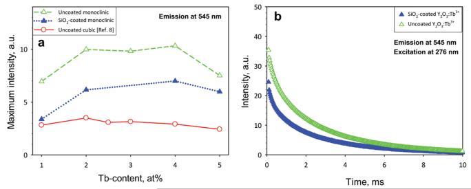
Figure 4a shows the maximum phosphorescence intensities of these nanophosphors as a function of Tb content. The highest intensity is obtained for a Tb content of 2–4 at % regardless of Y2O3 crystal phase or SiO2 coating, resulting from the increasing number of luminescent centers.30 Above 4 at % Tb content, energy transfer between adjacent luminescent centers to inactive sites occurs, leading to phosphorescence quenching.31 The uncoated monoclinic (open triangles) Y2O3:Tb3+ has higher phosphorescence for all Tb contents than both SiO2-coated monoclinic (filled triangles) and uncoated cubic8 (open circles) Y2O3 nanophosphors. The uncoated monoclinic nanophosphors have stronger phosphorescence than the SiO2-coated ones, most probably by the UV-light absorption and scattering32 of amorphous SiO2 that reduces the excitation irradiation intensity. The SiO2-coated monoclinic Y2O3:Tb3+ nanoparticles still outperform the uncoated cubic ones. This enables such biocompatible and easily dispersible nanoparticles to be employed in bioapplications without any adverse toxic effects, common with other light emitting nanoparticles that contain heavy metals (quantum dots).
Figure 4.
(a) The maximum phosphorescence intensity monitored at 545 nm under excitation of 276 nm for the uncoated cubic (solid line, open circles) from ref 8, uncoated monoclinic (broken line, open triangles), and SiO2-coated monoclinic (dotted line, filled triangles) nanoparticles as a function of Tb content. (b) Photoluminescence emission intensity decay curves of as-prepared, uncoated (open triangles), and SiO2-coated (filled triangles) Y2O3:Tb3+ (2 at % Tb) nanophosphors.
Figure 4b shows the decay profiles of the uncoated and SiO2-coated monoclinic Y2O3:Tb3+ (2 at % Tb) nanophosphors. Both profiles are similar, exhibiting the characteristic single exponential decay and indicating that the presence of the thin SiO2 shell does not significantly influence the luminescence of the core Y2O3:Tb3+ particles. The exponential decay time constants of luminescence for both as-prepared uncoated and SiO2-coated monoclinic Y2O3:Tb3+ (1–5 at %) nanophosphors had similar values and decreased from 2.72 to 1.66 ms for increasing Tb content and were slightly larger than those of cubic Y2O3:Tb3+ (from 2.67 to 1.09 ms)8 and in agreement with flame-made Y2O3:Eu3+ nanophosphors of similar sizes.13
For both uncoated nanophosphors (monoclinic and cubic), however, the maximum intensity achieved by the monoclinic (broken line, open triangles) Y2O3 was about thrice higher than that of cubic (solid line, open circles). This suggests that monoclinic Y2O3 favors the green emission from the Tb3+ ions. This is in contrast to the red emission from the Eu3+ activated Y2O3 (5D0 → 7F2)13 for which cubic Y2O3 is favorable. This emphasizes the effect of dopant composition on the luminescence of nanophosphors. The above result here is also in contrast to Y2O3:Tb3+ nanoparticles ~20–40 nm in diameter made by microemulsion22 and showing higher phosphorescence intensity for cubic than monoclinic Y2O3. This lower phosphorescence for monoclinic Y2O3 was attributed to the presence of volatile impurities that were formed during its wet synthesis.22 These impurities disappeared for higher annealing temperature and transformation of the monoclinic phase to the cubic.22 Thus, the low degree of crystallinity and the presence of impurities in wet-made nanophosphors hindered phosphorescence by monoclinic Y2O3:Tb3+. However, flame processes typically yield high-purity products33 with desired crystallinity13 that facilitate their luminescence.
Annealing of Uncoated and SiO2-Coated Monoclinic Y2O3:Tb3+ Nanoparticles
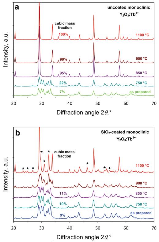
To further evaluate the effect of crystal structure on the luminescence of Y2O3:Tb3+ nanophosphors, an annealing study of the monoclinic Y2O3 nanoparticles was performed. Figure 5a shows the XRD patterns of uncoated monoclinic Y2O3:Tb3+ (2 at % Tb) annealed at 750, 850, 900, and 1100 °C for 10 h. The as-prepared monoclinic Y2O3 transforms completely to cubic above 850 °C consistent with the literature.22,27,34 With increasing temperature, the cubic phase is obtained while the estimated cubic crystal size increases from ~36 to ~90 nm, in line with the literature.27
Figure 5.
XRD patterns of the uncoated monoclinic (a) and SiO2-coated monoclinic (b) Y2O3:Tb3+ (2 at % Tb) for different annealing temperatures (750, 850, 900, and 1100 °C) for 10 h. For the uncoated nanoparticles, the transition from the monoclinic phase to cubic occurs for temperatures >850 °C, while the SiO2 coating prevents this transition significantly until 900 °C. The stars indicate peaks that correspond to yttrium-silicates.
The SiO2-coated Y2O3:Tb3+ nanoparticles (Figure 5b) retain their mostly monoclinic phase until 850 °C as well as their crystal size (dXRD = 22.5–25 nm), in contrast with the uncoated ones (Figure 5a). This indicates that the SiO2 shell inhibits the core crystal growth during annealing, as seen with silica-coated nanosilver.11 At 900 °C and above, a significant change in the XRD spectrum is observed. Apart from the formation of cubic Y2O3, also a few more peaks emerge (2θ = 23.3, 24.8, 26.7, 29.7, 30.8, 32.5, 46.2, 52.2, and 54.0°) that correspond neither to monoclinic nor cubic Y2O3 (Figure 5b, stars). These peaks most probably correspond to yttrium-silicates35 that were formed by the interaction of the SiO2 shell with the core crystal Y2O3 at this high temperature. This inhibits also the accurate estimation of the cubic and monoclinic crystal sizes and their mass fractions from the XRD spectra for temperatures above 850 °C.
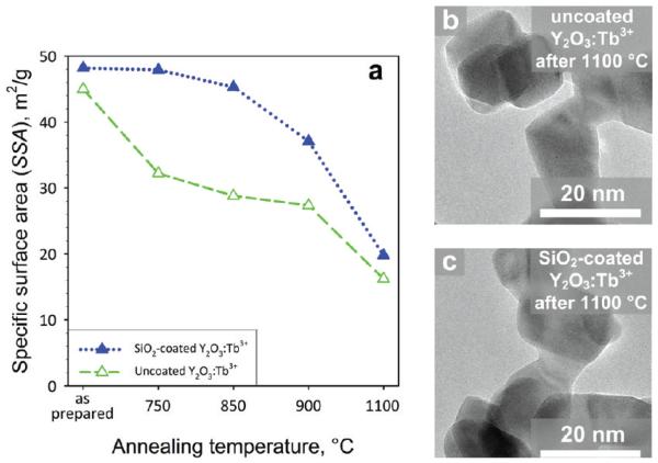
Figure 6a shows the specific surface area (SSA) as a function of annealing temperature for uncoated (open triangles) and SiO2-coated monoclinic Y2O3:Tb3+ (filled triangles) for 2 at % Tb-content, respectively. For the uncoated, the SSA monotonically decreases with annealing temperature with the formation of sinter necks27 (Figure 6b) and coalescence of particles, in agreement with the increase of crystal size (Figure 5a). The SSA for the SiO2-coated sample remains fairly constant up to 850 °C, so there is no significant increase in grain size. This indicates that the SiO2 coating inhibits the core crystal growth and has encapsulated fully the Y2O3 core particles. Furthermore, the SSA of the as-prepared, uncoated, and SiO2-coated nanoparticles is practically the same, indicating that there are no separate SiO2 nanoparticles formed that would lead to larger SSA values.24 For temperatures above 850 °C, however, the SSA decreases significantly and formation of sinter necks occurs (Figure 6c). No amorphous phase is detected by TEM, verifying the formation of the larger cubic Y2O3 crystal phase and the yttrium-silicates, in agreement with XRD (Figure 5b).
Figure 6.
(a) The specific surface area (SSA) as a function of the annealing temperature for the uncoated (open triangles) and SiO2-coated monoclinic (filled triangles) Y2O3:Tb3+ nanophosphors. TEM images of the uncoated (b) and SiO2-coated (c) Y2O3:Tb3+ after 1100 °C annealing.
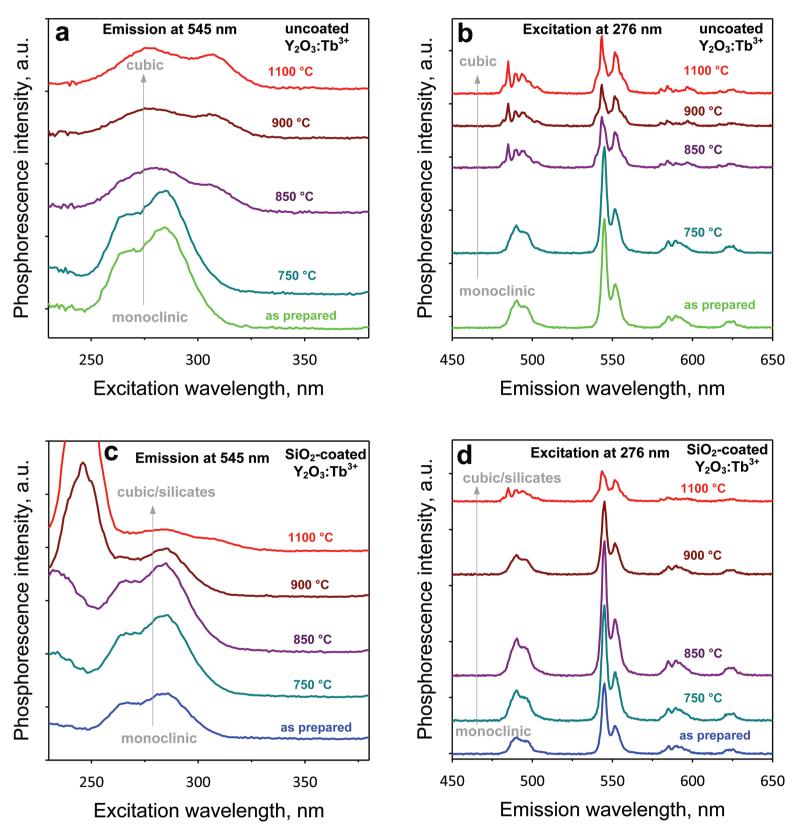
Figure 7a,b shows the excitation and emission spectra, respectively, of the annealed uncoated monoclinic Y2O3:Tb3+ (2 at % Tb) nanophosphors. For increasing annealing temperature, the monoclinic crystals transform to larger cubic ones (Figures 5a and 6a). Therefore, both excitation and emission spectra shift from monoclinic to cubic Y2O3. Figure 7b also shows that the emission phosphorescence intensity decreases with increasing annealing temperature and phase transformation, further indicating that the monoclinic Y2O3 crystal phase favors the green phosphorescence of Tb3+. Such a decrease in the phosphorescence for higher annealing temperatures has also been observed for other systems (SiO2:Tb3+) and has been attributed to the reduction of effective Tb3+ luminescent centers because of the formation of optically inactive Tb clusters.36
Figure 7.
The excitation monitored at 545 nm (a, c) and emission under 276 nm excitation (b, d) spectra of the 2 at % Tb-doped Y2O3 uncoated monoclinic (a, b) and SiO2-coated monoclinic (c, d) nanoparticles for the different annealing temperatures (750, 850, 900, and 1100 °C). The phosphorescence intensity decreases for the transition from monoclinic to cubic crystal structure.
Perhaps there is a better distribution of Tb3+ in the monoclinic Y2O3 host matrix because of its smaller size than cubic, facilitating the Tb3+ radiative transitions.36 Furthermore, the probability of the 5D4 → 7F5 electric-dipole transition of Tb3+ (responsible for the green color emission) contains contributions from linear and third order terms of the crystal lattice.20 Some of the crystal point groups in the cubic Y2O3 have no linear term, and therefore, a larger transition probability may be realized by embedding Tb3+ in lattice sites with crystals having linear terms,20 such as the monoclinic Y2O3 (with corresponding crystal point group Cs ).19
The excitation spectra of the SiO2-coated monoclinic Y2O3:Tb3+ (2 at % Tb) for increasing annealing temperature (Figure 7c) exhibit characteristic bands related to the monoclinic phase until 850 °C. This indicates that the SiO2 coating prevents the Y2O3 phase transformation, in agreement with XRD (Figure 5b). However, for annealing above 850 °C, an excitation band arises at quite low wavelength (<250 nm), which becomes the dominant one at 900 and 1100 °C. This band is most probably attributed to the interaction of the SiO2 coating with the core Y2O3:Tb3+ and the formation of yttrium-silicates. This band could be related to the excitation of the 7D energy level in the Tb3+ ion.36 Nonetheless, at 1100 °C, where there is cubic Y2O3:Tb3+ (Figure 5b), the excitation bands (centered at ~280 and ~310 nm) related to the cubic phase are also present.
This transformation from monoclinic to cubic can also be observed in the emission spectra of the SiO2-coated nanophosphors (Figure 7d), in which the reduction of the dominant peak occurs for the highest annealing temperature. Furthermore, the highest intensity at ~545 nm is obtained at 850 °C. At this temperature, the monoclinic phase (Figure 5b) and core size (dXRD = ~25 nm) are retained. Most likely annealing at this temperature has improved the core Y2O3:Tb3+ crystallinity and eliminated any Y2O3 crystal defects,22 increasing the phosphorescence intensity.27,37 This further indicates that monoclinic Y2O3 favors the Tb3+ phosphorescence.
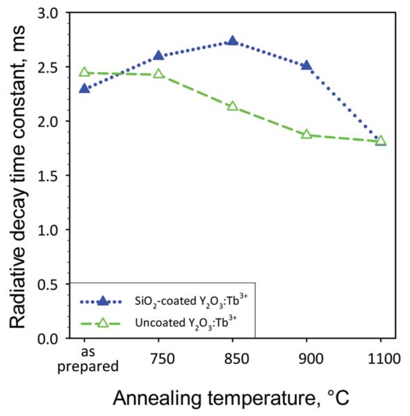
Figure 8 shows the radiative exponential decay time constants of the uncoated (open triangles) and SiO2-coated (filled triangles) Y2O3:Tb3+ (2 at % Tb) as a function of annealing temperature. The radiative decay time constants of both as-prepared nanophosphors are comparable, indicating a little effect on the luminescent properties by the SiO2 shell of the core Y2O3:Tb3+ nanophosphors. For increasing annealing temperature, the radiative decay time constant of the uncoated nanophosphors decreases monotonically as their size increases,27 in agreement with Figure 6. In contrast, the radiative decay time of the SiO2-coated nanophosphors slightly increases and remains at about the same level until 900 °C. At 1100 °C, however, the radiative decay time constant reaches similar values for both nanophosphors.
Figure 8.
The exponential decay time constants of luminescence for the uncoated (open triangles) and SiO2-coated (filled triangles) Y2O3:Tb3+ (2 at % Tb) as a function of the annealing temperature.
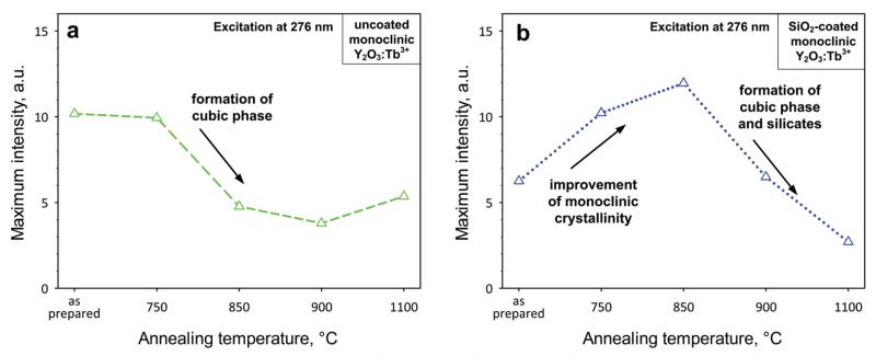
Figure 9 shows the maximum phosphorescence intensity of uncoated (a) and SiO2-coated (b) monoclinic Y2O3:Tb3+ (2 at % Tb) nanophosphors when excited at 276 nm at different annealing temperatures. For uncoated monoclinic nanophosphors (Figure 9a), the graph can be divided into two areas: one ≤750 °C in which there is no significant change and one >750 °C in which core crystal growth and phase transformation from monoclinic to cubic occurs and, thus, the maximum phosphorescence decreases. For the SiO2-coated nanophosphors (Figure 9b), the phosphorescence increases up to 850 °C because there is an improvement of the monoclinic phase and possibly elimination of any crystal defects while the SiO2 coating prevents crystal growth and phase transformation. Above 850 °C, a dramatic reduction in phosphorescence occurs that is attributed to formation of cubic Y2O3 and yttrium-silicates.
Figure 9.
The maximum phosphorescence intensity of the uncoated (a) and SiO2-coated (b) monoclinic Y2O3:Tb3+ (2 at % Tb) nanophosphors when excited at 276 nm for the different annealing temperatures.
IV. CONCLUSIONS
Terbium-doped Y2O3 nanophosphors (1–5 at % Tb) were made by flame spray synthesis and were dry-coated in situ by thin silica films. The optimum Tb content was 2–4 at % for both cubic and monoclinic Y2O3 nanophosphors. For the first time, to the best of our knowledge, it is shown that the phosphorescence intensity is higher for monoclinic Y2O3 rather than cubic. By annealing monoclinic nanophosphors, their phosphorescence was reduced as they were transformed to cubic. The SiO2 coating prevented the monoclinic core particle growth and phase transformation until 850 °C, while their crystallinity was improved by annealing that increased their phosphorescence. Therefore, monoclinic Y2O3 favors the green phosphorescence of Tb3+ ions, in contrast to the phosphorescence of the well-studied Eu3+ ions where there is higher phosphorescence for the cubic crystal structure. This understanding may facilitate synthesis of bright green nanophosphors with a biocompatible coating suitable for display and bioimaging applications.
ACKNOWLEDGMENTS
We thank Dr. Frank Krumeich (Electron Microscopy Center, ETH Zurich) for the electron microscopy analysis. Financial support by the Swiss National Science Foundation (No. 200020-126694) and European Research Council is kindly acknowledged.
Footnotes
The authors declare no competing financial interest.
REFERENCES
- (1).Justel T, Nikol H, Ronda C. Angew. Chem., Int. Ed. 1998;37:3085. doi: 10.1002/(SICI)1521-3773(19981204)37:22<3084::AID-ANIE3084>3.0.CO;2-W. [DOI] [PubMed] [Google Scholar]
- (2).Igarashi T, Ihara M, Kusunoki T, Ohno K, Isobe T, Senna M. Appl. Phys. Lett. 2000;76:1549. [Google Scholar]
- (3).Zhang F, Wong SS. ACS Nano. 2010;4:99. doi: 10.1021/nn901057y. [DOI] [PubMed] [Google Scholar]
- (4).Feldmann C, Justel T, Ronda CR, Schmidt P. J. Adv. Funct. Mater. 2003;13:511. [Google Scholar]
- (5).Ropp RC. J. Electrochem. Soc. 1964;111:311. [Google Scholar]
- (6).Bunzli JCG, Piguet C. Chem. Soc. Rev. 2005;34:1048. doi: 10.1039/b406082m. [DOI] [PubMed] [Google Scholar]
- (7).Anh TK, Ngoc T, Nga PT, Bich VT, Long P, Strek W. J. Lumin. 1988;39:215. [Google Scholar]
- (8).Sotiriou GA, Schneider M, Pratsinis SE. J. Phys. Chem. C. 2011;115:1084. doi: 10.1021/jp106137u. [DOI] [PMC free article] [PubMed] [Google Scholar]
- (9).Das GK, Tan TTY. J. Phys. Chem. C. 2008;112:11211. [Google Scholar]
- (10).Sotiriou GA, Hirt AM, Lozach PY, Teleki A, Krumeich F, Pratsinis SE. Chem. Mater. 2011;23:1985. doi: 10.1021/cm200399t. [DOI] [PMC free article] [PubMed] [Google Scholar]
- (11).Sotiriou GA, Sannomiya T, Teleki A, Krumeich F, Vörös J, Pratsinis SE. Adv. Funct. Mater. 2010;20:4250. doi: 10.1002/adfm.201000985. [DOI] [PMC free article] [PubMed] [Google Scholar]
- (12).Sotiriou GA, Pratsinis SE. Environ. Sci. Technol. 2010;44:5649. doi: 10.1021/es101072s. [DOI] [PubMed] [Google Scholar]
- (13).Camenzind A, Strobel R, Pratsinis SE. Chem. Phys. Lett. 2005;415:193. [Google Scholar]
- (14).Konrad A, Fries T, Gahn A, Kummer F, Herr U, Tidecks R, Samwer K. J. Appl. Phys. 1999;86:3129. [Google Scholar]
- (15).Konrad A, Herr U, Tidecks R, Kummer F, Samwer K. J. Appl. Phys. 2001;90:3516. [Google Scholar]
- (16).Ray S, Pramanik P, Singha A, Roy A. J. Appl. Phys. 2005;97:094312. [Google Scholar]
- (17).Qin X, Ju YG, Bernhard S, Yao N. J. Mater. Res. 2005;20:2960. [Google Scholar]
- (18).Dhanaraj J, Jagannathan R, Kutty TRN, Lu CH. J. Phys. Chem. B. 2001;105:11098. [Google Scholar]
- (19).Gozzi D, Latini A, Salviati G, Armani N. J. Appl. Phys. 2006;99:123524. [Google Scholar]
- (20).Hoshina T. Jpn. J. Appl. Phys. 1967;6:1203. [Google Scholar]
- (21).Wang L, Pan YX, Ding Y, Yang WG, Mao WL, Sinogeikin SV, Meng Y, Shen GY, Mao HK. Appl. Phys. Lett. 2009;94:061921. [Google Scholar]
- (22).Graeve OA, Corral JO. Opt. Mater. 2006;29:24. [Google Scholar]
- (23).Ishiwada N, Ueda T, Yokomori T. Luminescence. 2011;26:381. doi: 10.1002/bio.1237. [DOI] [PubMed] [Google Scholar]
- (24).Teleki A, Heine MC, Krumeich F, Akhtar MK, Pratsinis SE. Langmuir. 2008;24:12553. doi: 10.1021/la801630z. [DOI] [PubMed] [Google Scholar]
- (25).Teleki A, Suter M, Kidambi PR, Ergeneman O, Krumeich F, Nelson BJ, Pratsinis SE. Chem. Mater. 2009;21:2094. [Google Scholar]
- (26).Kubrin R, Tricoli A, Camenzind A, Pratsinis SE, Bauhofer W. Nanotechnology. 2010;21:225603. doi: 10.1088/0957-4484/21/22/225603. [DOI] [PubMed] [Google Scholar]
- (27).Camenzind A, Strobel R, Krumeich F, Pratsinis SE. Adv. Powder Technol. 2007;18:5. [Google Scholar]
- (28).Meng QY, Chen BJ, Xu W, Yang YM, Zhao XX, Di WH, Lu SZ, Wang XJ, Sun JS, Cheng LH, Yu T, Peng Y. J. Appl. Phys. 2007;102:093505. [Google Scholar]
- (29).Ray S, Patra A, Pramanik P. Opt. Mater. 2007;30:608. [Google Scholar]
- (30).Blasse G. Mater. Chem. Phys. 1987;16:201. [Google Scholar]
- (31).Blasse G, Grabmaier BC. Luminescent Materials. Springer; Berlin: 1994. [Google Scholar]
- (32).Fu Y-X, Sun Y-H. J. Alloys Compd. 2009;471:190. [Google Scholar]
- (33).Pratsinis SE. AIChE J. 2010;56:3028. [Google Scholar]
- (34).Zhang P, Navrotsky A, Guo B, Kennedy I, Clark AN, Lesher C, Liu QY. J. Phys. Chem. C. 2008;112:932. [Google Scholar]
- (35).Rakov N, Amaral DF, Guimaraes RB, Maciel GS. J. Appl. Phys. 2010;108:073501. [Google Scholar]
- (36).Sun JM, Skorupa W, Dekorsy T, Helm M, Rebohle L, Gebel T. J. Appl. Phys. 2005;97:123513. [Google Scholar]
- (37).Pradhan AK, Zhang K, Mohanty S, Dadson J, Hunter D, Loutts GB, Roy UN, Cui Y, Burger A, Wilkerson AL. J. Appl. Phys. 2005;97:023513. [Google Scholar]


