Abstract
The lack of a bandgap makes bulk graphene unsuitable for room temperature transistors with a sufficient on/off current ratio. Lateral constriction of charge carriers in graphene nanostructures or vertical inversion symmetry breaking in bilayer graphene are two potential strategies to mitigate this challenge, but each alone is insufficient to consistently achieve a large enough on/off ratio (e.g. > 1000) for typical logic applications. Herein we report the combination of lateral carrier constriction and vertical inversion symmetry breaking in bilayer graphene nanoribbons (GNRs) to tune their transport gaps and improve the on/off ratio. Our studies demonstrate that the on/off current ratio of bilayer GNRs can be systematically increased upon applying a vertical electric field, to achieve a largest on/off current ratio over 3000 at room temperature.
Graphene has attracted considerable interest as a new electronic material for both fundamental investigations and potential applications due to its unique electronic properties including the highest room temperature carrier mobility and carrier saturation velocity of all known materials1,2,3,4,5. However, the bulk graphene sheet is a semimetal with a zero bandgap and cannot be used for room temperature transistors with sufficient on/off ratio, which remains a main challenge to apply graphene for digital electronic or photonic applications6,7. A number of approaches have been proposed for inducing a bandgap in mono- or bilayer graphene. A first strategy is to create graphene nanostructures with lateral constriction and confinement of charge carriers8,9,10,11,12,13,14,15,16,17,18,19. In particular, graphene nanoribbons (GNRs) of sub-10 nm width are predicted to be semiconducting due to lateral confinement of the electron wave function in the transverse direction and edge disorder induced Anderson localization. Both theoretical and experimental studies have demonstrated that Anderson localization along with lateral confinement can be achieved in GNRs8,9,10,11,12,13,14,15,16,17,18, nanomeshes19, or quantum dots20 to open up a transport gap inversely proportional to the conducting channel width. An on/off ratio up to 100 is typically achieved at room temperature in these graphene nanostructures with occasionally larger values achieved in ultra-small devices17,19,20. An alternative strategy is to break the inversion symmetry in bilayer graphene21,22,23,24,25. By applying external electric field normal to the bilayer graphene plane, band gap can be opened in the Bernal-stacking (AB-stacking) bilayer graphene. In particular, bilayer graphene field effect transistors (FETs) with on/off ratio up to 100 have been achieved at the room temperature24.
The combination of both methods together has the potential to open up a larger bandgap in bilayer GNRs. The theoretical studies have suggested that a vertical field could be used to further modulate the band gap in a bilayer or tri-layer GNRs26,27,28,29, but there is yet a lack of experimental investigation on this topic to date. Herein, we report the first experimental demonstration that a combination of lateral carrier constriction and vertical inversion symmetry breaking in bilayer GNRs can be used to achieve graphene devices with further improved on/off ratios. We show that the on/off current ratio of bilayer GNRs can be increased greatly to reach up to 3000 at room temperature by applying a vertical electric field. This on/off current ratio of our bilayer GNR FET is 30 fold higher than the highest value (~100) reported previously for bilayer graphene devices24.
Results
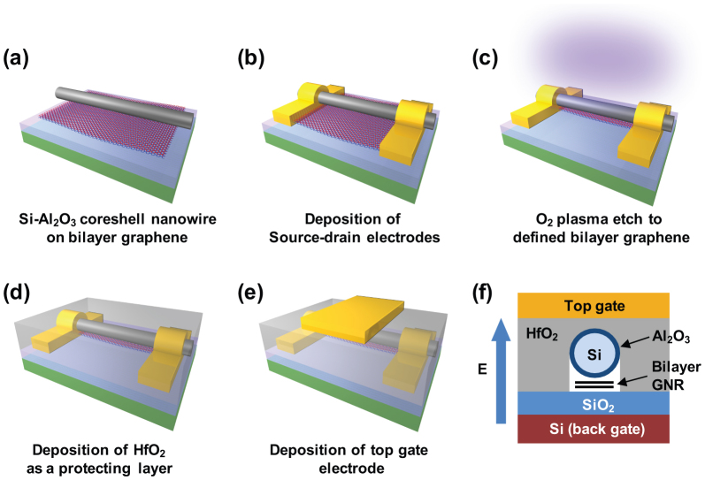
Bilayer GNRs were produced by employing thin nanowires as a physical protection mask in oxygen plasma etching process. Figure 1 illustrates the fabrication steps to obtain dual gated bilayer GNR FETs. Bilayer graphene on the silicon substrate was prepared as a starting material through exfoliation from natural graphite and physical dry transfer process, although the approach described here can be readily extended to graphene sheets or films obtained through chemical approaches29,30,31,32. The layers of graphene were classified based on their optical contrast and Raman spectroscopic studies (Fig. S1)33,34. The Si/Al2O3 core/shell nanowires were then aligned on top of bilayer graphene through a physical dry transfer process (Fig. 1a)35,36, followed by the definition of source and drain electrodes (Ti/Au: 30 nm/60 nm) using e-beam lithography and e-beam evaporation (Fig. 1b). The Si/Al2O3 core/shell nanowires were produced by deposition of 2 nm Al2O3 on the Si nanowire surface using an atomic layer deposition (ALD) process. TEM studies show a uniformly coated Al2O3 layer on Si nanowire surface (Fig. S2a, b). The Si/Al2O3 nanowire mask is not removed from the device, and the resistance of the nanowire itself is typically larger than 1 tera-ohm and would not affect the charge transport of the final devices (Fig. S2c, d). Oxygen plasma was used to remove the exposed graphene, leaving only the graphene protected underneath the Si/Al2O3 nanowire to form a GNR connected to two big blocks of graphene protected under the source and drain electrodes (Fig. 1c)17. A 60 nm HfO2 protecting layer was then deposited on the top of device using e-beam evaporation to prevent electrical breakdown of the oxygen plasma damaged SiO2 back gate dielectric under high field (Fig. 1d). It was found that SiO2 back gate dielectric (after exposure to oxygen plasma) can be easily broken down by the relatively high vertical electric field (e.g. at VBG ~50 V). The typical breakdown voltage was increased to VBG ~120V with the deposition of the HfO2 protecting layer. Lastly, top gate electrode of (Ti/Au: 30 nm/60 nm) was fabricated using conventional e-beam lithography (Fig. 1e). Figure 1f shows cross sectional view of dual-gated bilayer GNR FET. In this device, heavily n-doped silicon wafer was used as a back gate and 300 nm of SiO2 on the silicon wafer was used as back gate dielectric. Bilayer GNR is located underneath of Si-Al2O3 core-shell nanowire, and channel width of bilayer GNR is defined by nanowire diameter. Top gate dielectric consists of Si/Al2O3 core/shell nanowire and e-beam evaporation deposited HfO2. Top gate electrode is located on the top dielectric. Vertical electric field is applied between top and back gates to break the symmetry of bilayer GNR. Optical images of each fabrication steps are shown in Figure S3.
Figure 1. Schematic illustration of the fabrication procedures to obtain dual-gated bilayer graphene nanoribbon FET.
(a), Si/Al2O3 core/shell nanowires are transferred onto a bilayer graphene sheet. (b), Source and drain electrodes are formed on aligned bilayer graphene and Si/Al2O3 core/shell nanowires. (c), Uncovered bilayer graphene is etched by oxygen plasma, and bilayer graphene nanoribbons are produced underneath Si nanowires. (d), A thin film of 60 nm HfO2 is deposited by e-beam evaporation to prevent electrical breakdown of plasma damaged SiO2. (e), Top gate electrode is deposited as a final process. (f), Schematic of the cross-sectional view of the device.
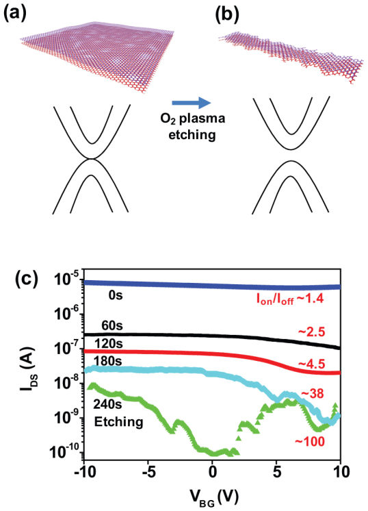
Channel narrowing was used as a first step to open up a transport gap in bilayer graphene (Fig. 2). Large area bilayer graphene is a semimetal with zero bandgap (Fig. 2a). A transport gap can be opened by etching large area graphene into one dimensional graphene nanoribbons due to the lateral confinement of the electron wave function in the transverse direction and edge disorder induced Anderson localization (Fig. 2b)8,9,10,11,12,13,14,15,16,17,18,19. Our previous studies have shown that the initial etching is predominantly a vertical etch and can result in GNRs with width comparable to the nanowire diameter17. In our bilayer graphene FET, channel width was reduced from ~2.5 μm to ~40 nm of nanowire diameter after 60 s plasma etching. At the same time, on-current was significantly reduced from ~85 μA to ~250 nA and off-current was decreased from 60 μA to 100 nA, with the corresponding on/off current ratio improved from 1.4 to ~2.5 (Fig. 2c). The width of the GNRs can be further scaled down with additional etching steps that undercut the graphene underneath the nanowire through lateral etching17. The transfer characteristics of bilayer graphene nanoribbon show that the on/off current ratio of bilayer GNR FET was gradually improved from ~2.5 to ~100 with increasing etching time from 60 s to 240 s in steps of 60 s (Fig. 2c). It should be noted that the I–V characteristics of our bilayer GNR FET is rather rough, which might be attributed to the edge disorder in narrow GNRs created by plasma etching process37. In general, electrical noise increases with narrowing channel width and increasing etching time (Fig. 2c).
Figure 2. The opening of transport gap in bilayer graphene by narrowing channel width.

(a–b), Schematic images of (a), bilayer graphene sheet and (b), bilayer graphene nanoribbon with corresponding band diagrams. (c), Transfer characteristics of a bilayer GNR FET at the various oxygen plasma etching time (VDS = 0.1 V). The etching time was varied from 0 s to 240 s from top to bottom in steps of 60 s.
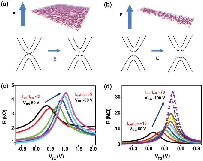
To further increase the transport bandgap and improve the on/off current ratio, vertical electric field was applied across the bilayer GNR to break the inversion symmetry (Fig. 3). Figure 3a schematically illustrates the change of the band gap of bilayer graphene upon application of vertical electric field. Bilayer graphene has a gapless band structure that valence and conduction bands have a point contact at the K point. If an electric field is applied perpendicular to the bilayer graphene, conduction band and valence band curves upwards and downwards near the K point, respectively, and a finite bandgap is created (Fig. 3a)38. It has been theoretically predicted that conduction and valence band of bilayer GNR can be tuned in a similar way to those of bilayer graphene sheet under a vertical electric field (Fig. 3b)26,27. In this way, a significantly larger bandgap can be achieved in bilayer GNRs than the bulk bilayer graphene sheet under the same vertical electric field. Figure 3c shows the switching characteristics of a bulk bilayer graphene FET with 2.7 μm wide by 4.5 μm long channel. Each curves was obtained by sweeping the top gate bias (VTG) from −0.7 to 2.1 V with a fixed drain-source bias (VDS) of 100 mV and variable back gate bias (VBG) from 60 to −90 V at steps of 30 V. The off-resistance increases in both directions of back gate voltage, which is consistent with previous reports on bilayer graphene devices24. The on/off ratio was improved from 2 to 5 by changing VBG from 60 V to −90 V. Figure 3d shows the switching characteristics of a bilayer GNR FET with a ~20 nm channel width, ~1.5 μm length, at a constant VDS of 100 mV and variable VBG from 60 to −100 V at steps of 20 V. The on/off current ratio was initially ~10 which is higher than graphene sheet in Figure 3c because of lateral confinement and edge disorder induced Anderson localization, and improved to ~70 by changing VBG from 60 to −100 V by the breaking inversion symmetry. This result is well matched with theoretical prediction of bandgap structures evolution as illustrated in Figure 3b.
Figure 3. The further opening of transport gap in bilayer graphene nanoribbon by breaking the inversion symmetry.
(a–b), Schematic images of (a), bilayer graphene sheet and (b), bilayer graphene nanoribbon with a vertical electrical displacement field and corresponding energy band structure before and after applying the displacement field. (c), Switching behavior of a bilayer graphene sheet FET at VDS = 0.1 V and VBG varied from 60 to −90 V in steps of 30 V. (d), Switching behavior of a bilayer graphene nanoribbon FETs at VDS = 0.1 V and VBG varied from 60 to −100 V in steps of 20 V.
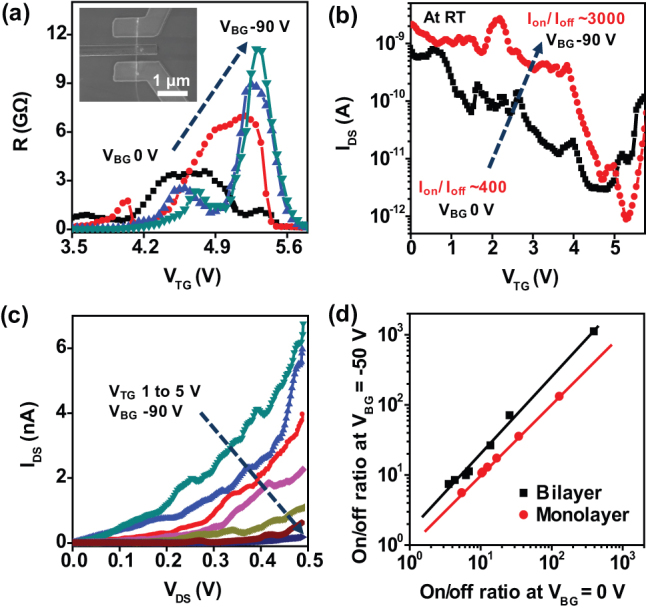
The final on/off current ratio of the bilayer GNR FET upon application of the vertical electric field is highly dependent on the initial on/off ratio without vertical electric field. We have studied gap opening in bilayer GNR with an initially high on/off current ratio of ~400 (Fig. 4). Figure 4a shows the switching behaviour of the bilayer GNR FET measured at room temperature. VTG was scanned from 0 V to 6 V while the VBG was varied from 0 to −90 V at steps of 30 V. This bilayer GNR FET showed an expected increase in off-resistance with increasing back gate voltage. Importantly, the transfer characteristics show the on/off current ratio was significantly improved from ~400 to > 3000 at room temperature (Fig. 4b). This represents the highest room-temperature on/off current ratio reported for bilayer graphene and is 30 fold higher than the highest value (~100) reported previously24. Figure 4c shows the output characteristics of the same device at variable VTG and a fixed VBG of −90V. The transport gap of the bilayer GNR FET can be estimated to be ~400 meV at the VBG = −90 V based on the relation Ion/Ioff ≈ exp(−qφbarrier/kBT) and Eg = 2qφbarrier, assuming the schottky barrier height is about half of the electrical bandgap (Fig. S4)18,24,39. Here, φbarrier is the schottky barrier height, kB is the Boltzmann constant, T is the temperature, and Eg is the bandgap.
Figure 4. High on/off ratio bilayer graphene nanoribbon FET.

(a–b), The room temperature (a), switching behavior and (b), transfer characteristics of the narrow bilayer graphene nanoribbon FET at the various back gate voltages (VDS = 10 mV). VBG was modulated from 0 to −90 V in steps of 30 V. Inset in (a) shows SEM image of the bilayer graphene nanoribbon FET used in this measurement. (c), IDS-VDS output characteristics of the narrow bilayer graphene nanoribbon FET with VTG varied from 1 to 5 V in steps of 0.5 V (VBG = −90 V). (d), Relations between the on/off current ratio of monolayer and bilayer GNR FETs before and after application of the vertical electric field. The vertical and horizontal axes indicate that the on/off current ratio before and after the application of the vertical electric field.
We have investigated a large number of monolayer and bilayer GNR devices. The on/off current ratio of bilayer GNRs (black square) and monolayer GNRs (red circle) FETs at the VBG = −50 V are plotted against the on/off current ratio at the VBG = 0 V (Fig. 4d). The plot clearly shows that the on/off current ratio of monolayer GNR FETs is not changed by application of vertical electric field (Fig. 4d, S5). On the other hand, all of the bilayer GNR FETs showed an obvious increase in on/off current ratios upon the application of a vertical electric field. The final on/off current ratio of bilayer GNR FETs are highly dependent on its initial on/off ratio.
Discussion
We have demonstrated that a larger transport gap can be induced in bilayer GNRs by combining two strategies of lateral constriction of charge carriers and vertical inversion symmetry breaking. A highest room temperature on/off current ratio over 3000 can be achieved upon applying a vertical electric field across a bilayer GNR with an initial on/off ratio of 400. This on/off ratio greatly exceeds the typical values obtained in graphene nanostructures or bilayer graphene devices, and is already large enough for logical applications. We should also note that although a highest on/off ratio exceeding 3000 is achieved, most of devices showed low on/off ratio around 100 or smaller. Importantly, our studies demonstrate that the on/off current ratio of the bilayer GNRs can be consistently improved upon the application of a vertical electric field, and the final on/off ratio of the bilayer GNRs with the vertical field is highly dependent on the initial on/off ratio without the vertical field. The on/off ratio of the bilayer GNR devices can be further enhanced through several strategies. First, the current devices do not have an effective alignment between the source-gate-drain electrodes, with the gate only modulate ~50% of the channel. A better alignment of source, drain, and gate electrodes can not only improve gate modulation of bilayer GNR device but also enhance the inversion-symmetry breaking in bilayer graphene. Secondly, the on-current of the graphene transistors can also be enhanced by reducing the graphene-metal contact resistance. The off-current can be further suppressed by improving the overall gate dielectric constant. Finally, the on/off ratio strongly depends on the ribbon width. Compared to wider GNR devices with similar channel lengths, sub-10 nm GNRs can exhibit greatly increased on/off ratio. Therefore, the on/off ratio can be further increased by using smaller mask nanowires to create smaller bilayer GNRs. Our study demonstrates that the lateral confinement and vertical inversion symmetry breaking can work synergistically in bilayer GNRs to open up an effective pathway to graphene devices with sufficient on/off ratio for logic applications, and can impact significantly in areas including digital electronics, nanophotonics, and terahertz technology.
Methods
Fabrication and characterization of the Bilayer GNR devices
The silicon nanowires used here were grown by the Au nanocluster mediated vapour-liquid-solid growth approach, with the diamerters typically in the range of 30–60 nm and lengths of around 10 μm. Al2O3 outer shell was coated through atomic layer deposition (ALD) on the Si nanowire surface. Si/Al2O3 core/shell nanowires were transferred by simply attaching nanowire grown wafer to target wafer. Nanowires were transferred onto target wafer surface by van der Waals force between the nanowires and the graphene surface. The fabrication method of bilayer GNR FETs is described in the main text. The d.c. electrical transport studies were conducted with a probe station at room temperature (25°C) under ambient conditions with a computer-controlled analogue-to-digital converter. SEM imaging was performed on a JEOL 6700F unit operated at 5 kV.
Author Contributions
X.D. and W.J.Y. conceived and designed the experiments. W.J.Y. performed the experiments. X.D. and W.J.Y. analysed the data and co-wrote the paper.
Supplementary Material
Supporting information
Acknowledgments
We acknowledge the Nanoelectronics Research Facility (NRF) at UCLA for technical support. X.D. acknowledges financial support by NSF CAREER award 0956171. W.J.Y. acknowledges partial support by the National Research Foundation of Korea Grant funded by the Korean Government (Ministry of Education, Science and Technology) [NRF-2011-351-c00034].
References
- Novoselov K. S. et al. Electric field effect in atomically thin carbon films. Science 306, 666–669 (2004). [DOI] [PubMed] [Google Scholar]
- Novoselov K. S. et al. Two-dimensional gas of massless Dirac fermions in graphene. Nature 438, 197–200 (2005). [DOI] [PubMed] [Google Scholar]
- Dean C. R. et al. Boron nitride substrates for high-quality graphene electronics. Nat. Nanotechnol 5, 722–726 (2010). [DOI] [PubMed] [Google Scholar]
- Wu Y. Q. et al. High-frequency, scaled graphene transistors on diamond-like carbon. Nature 472, 74–78 (2011). [DOI] [PubMed] [Google Scholar]
- Liao L. et al. High-speed graphene transistors with a self-aligned nanowire gate. Nature 467, 305–308 (2010). [DOI] [PMC free article] [PubMed] [Google Scholar]
- Wang F. et al. Gate-variable optical transitions in graphene. Science 320, 206–209 (2008). [DOI] [PubMed] [Google Scholar]
- Xia F., Mueller T., Lin Y.-M., Valdes-Garcia A. & Avouris Ph. Ultrafast graphene photodetector. Nat. Nanotechnol. 4, 839–843 (2009). [DOI] [PubMed] [Google Scholar]
- Han M. Y., Brant J. C. & Kim P. Electron transport in disordered graphene nanoribbons. Phys. Rev. Lett. 104, 056801 (2010). [DOI] [PubMed] [Google Scholar]
- Gunlycke D., Areshkin D. A. & White C. T. Semiconducting graphene nanostrips with edge disorder. Appl. Phys. Lett. 90, 142104 (2007). [Google Scholar]
- Lherbier A. et al. Transport length scales in disordered graphene-based materials: strong localization regimes and dimensionality effects. Phys. Rev. Lett. 100, 036803 (2008). [DOI] [PubMed] [Google Scholar]
- Evaldsson M. et al. Edge-disorder-induced Anderson localization and conduction gap in graphene nanoribbons. Phys. Rev. B 78, 161407(R) (2008). [Google Scholar]
- Querlioz D. et al. Suppression of the orientation effects on bandgap in graphene nanoribbons in the presence of edge disorder. Appl. Phys. Lett. 92, 042108 (2008). [Google Scholar]
- Mucciolo E. R., Castro Neto A. H. & Lewenkopf C. H. Conductance quantization and transport gaps in disordered graphene nanoribbons. Phys. Rev. B 79, 075407 (2009). [Google Scholar]
- Martin I. & Blanter Y. M. Transport in disordered graphene nanoribbons. Phys. Rev. B 79, 235132 (2009). [Google Scholar]
- Han M. Y., Ozyilmaz B., Zhang Y. & Kim P. Energy band-gap engineering of graphene nanoribbons. Phys. Rev. Lett. 98, 206805 (2007). [DOI] [PubMed] [Google Scholar]
- Li X., Wang X., Zhang L., Lee S. & Dai H. Chemically derived, ultrasmooth graphene nanoribbon semiconductors. Science 319, 1229–1232 (2008). [DOI] [PubMed] [Google Scholar]
- Bai J., Duan X. & Huang Y. Rational fabrication of graphene nanoribbons using a nanowire etch mask. Nano Lett. 9, 2083–2087 (2009). [DOI] [PubMed] [Google Scholar]
- Wang X. & Dai H. Etching and narrowing of graphene from the edges. Nat. Chem. 2, 661–665 (2010). [DOI] [PubMed] [Google Scholar]
- Bai J., Zhong X., Jiang S., Huang Y. & Duan X. Graphene nanomesh. Nat. Nanotechnol. 5, 190–194 (2010). [DOI] [PMC free article] [PubMed] [Google Scholar]
- Ponomarenko L. A. et al. Chaotic dirac billiard in graphene quantum dots. Science 320, 356 (2008). [DOI] [PubMed] [Google Scholar]
- Zhang Y. et al. Direct observation of a widely tunable bandgap in bilayer graphene. Nature 459, 820–823 (2009). [DOI] [PubMed] [Google Scholar]
- Castro E. V. et al. Biased bilayer graphene: semiconductor with a gap tunable by the electric field effect. Phys. Rev. Lett. 99, 216802 (2007). [DOI] [PubMed] [Google Scholar]
- Ohta T., Bostwick A., Seyller Th., Horn K. & Rotenberg E. Controlling the electronic structure of bilayer graphene. Science 313, 951–954 (2006). [DOI] [PubMed] [Google Scholar]
- Xia F., Farmer D. B., Lin Y. & Avouris Ph. Graphene field-effect transistors with high on/off current ratio and large transport bandgap at room temperature. Nano Lett. 10, 715–718 (2010). [DOI] [PubMed] [Google Scholar]
- Yu W. J., Liao L., Chae S. H., Lee Y. H. & Duan X. Toward tunable bandgap and tunable dirac point in bilayer graphene with molecular doping. Nano Lett. 11, 4759–4763 (2011). [DOI] [PMC free article] [PubMed] [Google Scholar]
- Sahu B., Min H., MacDonald A. H. & Banerjee S. K. Energy gaps, magnetism, and electric-field effects in bilayer graphene nanoribbons. Phys. Rev. B 78, 045404 (2008). [Google Scholar]
- Lima M. P., Fazzio A. & Silva A. J. R. Edge effects in bilayer graphene nanoribbons: Ab initio total-energy density functional theory calculations. Phys. Rev. B 79, 153401 (2009). [Google Scholar]
- Kumar B. & Guo J. Multilayer graphene nanoribbon under vertical electric field. J. Appl. Phys. 110, 044309 (2011). [Google Scholar]
- Park S. & Ruoff R. S. Chemical methods for the production of graphenes. Nat. Nanotechnol. 4, 217–224 (2009). [DOI] [PubMed] [Google Scholar]
- Tung V. C., Allen M. J., Yang Y. & Kaner R. B. High-throughput solution processing of large-scale graphene. Nat. Nanotechol. 4, 25–29 (2009). [DOI] [PubMed] [Google Scholar]
- Li X. et al. Large-area synthesis of high quality and uniform graphene films on copper foils. Science 324, 1312–1314 (2009). [DOI] [PubMed] [Google Scholar]
- Reina A. et al. Large area, few-layer graphene films on arbitrary substrates by chemical vapour deposition. Nano Lett. 9, 30–35 (2009). [DOI] [PubMed] [Google Scholar]
- Blake P. et al. Making graphene visible. Appl. Phys. Lett. 91, 063124 (2007). [Google Scholar]
- Ferrari A. C. et al. Raman spectrum of graphene and graphene layers. Phy. Rev. Lett. 97, 187401 (2006). [DOI] [PubMed] [Google Scholar]
- Liao L. et al. High-kappa oxide nanoribbons as gate dielectrics for high mobility top-gated graphene transistors. Proc. Natl. Acad. Sci. USA 107, 6711–6715 (2010). [DOI] [PMC free article] [PubMed] [Google Scholar]
- Liao L. et al. Top-gated graphene nanoribbon transistors with ultrathin high-k dielectrics. Nano Lett. 10, 1917–1921 (2010). [DOI] [PMC free article] [PubMed] [Google Scholar]
- Yang R., Shi Z., Zhang L., Shi D. & Zhang G. Observation of raman G-peak split for graphene nanoribbons with hydrogen-terminated zigzag edges. Nano Lett. 11, 4083–4088 (2011). [DOI] [PubMed] [Google Scholar]
- Schwierz F. Graphene transistors. Nat. Nanotechnol. 5, 487–496 (2010). [DOI] [PubMed] [Google Scholar]
- Bai J. et al. Very large magnetoresistance in graphene nanoribbons. Nat. Nanotechnol. 5, 655–659 (2010). [DOI] [PMC free article] [PubMed] [Google Scholar]
Associated Data
This section collects any data citations, data availability statements, or supplementary materials included in this article.
Supplementary Materials
Supporting information


