Rational control over the morphology and the functional properties of inorganic nanostructures has been a long-standing goal in the development of bottom-up device fabrication processes. We report that the geometry of hydrothermally grown zinc oxide nanowires (ZnO NWs)1–4 can be tuned from platelets to needles, covering more than three orders of magnitude in aspect ratio (~0.1–100). We introduce a classical thermodynamics-based model to explain the underlying growth inhibition mechanism via the competitive and face-selective electrostatic adsorption of non-zinc complex ions at alkaline conditions. The performance of these NWs rivals that of vapor-phase-grown nanostructures5–6, and their low-temperature synthesis (<60°C) is favorable to the integration and in-situ fabrication of complex and polymer-supported devices7–9. We illustrate this capability by fabricating an all-inorganic light-emitting diode in a polymeric microfluidic manifold. Our findings indicate that electrostatic interactions in aqueous crystal growth may be systematically manipulated to synthesize nanostructures and devices with enhanced structural control.
As a low temperature aqueous process, hydrothermal synthesis1–3,10–12 or crystallization from supersaturated aqueous solutions3,10 holds great promise for nanostructure synthesis on a variety of substrates, and to date has been reported in the construction of several energy harvesting- and electronic devices13–14. The functions of these devices are critically linked to nanostructure morphology and hence require parameter tuning for optimal performance. Therefore, a predictive model-based hydrothermal synthesis that enables the rational control over nanostructure morphology would greatly catalyze bottom-up nanoscience. To this end, many growth parameters have been previously explored to manipulate the morphology of hydrothermally synthesized ZnO nanowires3,10, including the addition of auxiliary agents such as organic ligands and metal ion impurities2,4,12,14–15. Previous findings that pH-dependent electrostatic interactions between zinc reactants and the crystal can influence the preferred growth direction2,11,16–17 suggest that such interactions may provide a potential modality of control over ZnO nanowire morphology. Expanding upon these explorations, a rational approach to systematically alter nanowire morphology bi-directionally (i.e. increase or decrease aspect ratio) via electrostatics was developed here.
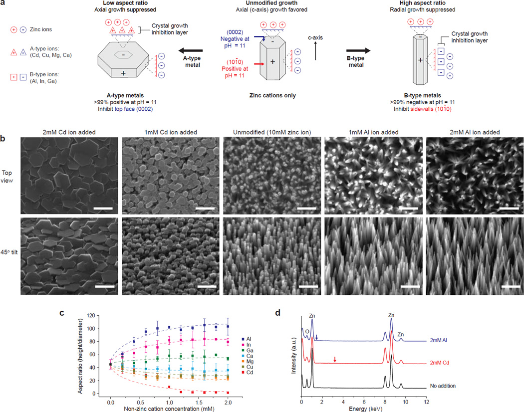
The primary principle underlying the rational control during hydrothermal synthesis is face-selective electrostatic interaction. By introducing ancillary non-zinc sulfates into this reaction, we are able to systematically control the local reaction environment during the growth phase. The non-zinc ions form charged but largely unreactive complexes that can localize to the oppositely charged crystal surfaces, thereby competitively limiting the access of the reactive zinc intermediates and inhibiting growth in a crystal face-specific manner (Fig. 1). This mechanism is supported by classical thermodynamic modeling provided here, and validated by the ability to predict the effect of introducing various non-zinc ions on the aspect ratio of ZnO NWs. The further understanding of electrostatics in controlled aqueous growth may enhance the syntheses of other inorganic structures, such as biomineralized and biomimetically crystallized nanostructures18–19, or in-situ grown layer-by-layer assemblies20.
Figure 1. Rational control over zinc oxide nanowire morphology via face-selective electrostatic crystal growth inhibition.
(a) Mechanism of control by non-zinc metal sulfates in the bath solution. A-type cations (positive at pH 11; Cd, Cu, Mg, and Ca) suppress axial growth at the negative (0002) face by limiting zinc complex-ion access, thus promoting platelet formation. Similar interaction between B-type ions (negative at pH 11; Al, In, Ga) and the positive (101̅1) sidewalls lead to high-aspect ratio nanowires. (b) SEM of ZnO nanowires grown in the presence of Cd or Al. Scale bar = 500nm. (c) The aspect ratio was tunable with >1000-fold range (mean ± one standard deviation). Dotted trend lines are to guide the eye. d) Energy dispersive x-ray spectra of nanowires grown in the presence of 2mM Al or Cd lack readily observable Al (blue arrow, 1.49 keV) or Cd (red arrow, 3.13 keV) peaks.
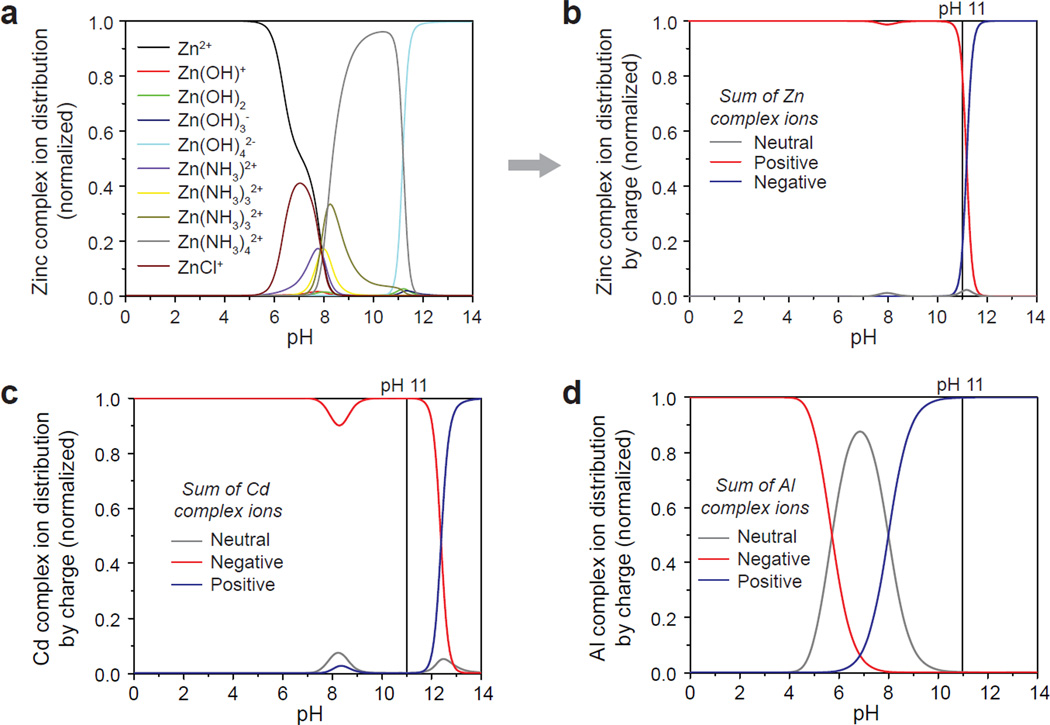
Single-crystalline nanowires were grown on substrates with zinc oxide seed layers in aqueous solutions of 10mM zinc sulfate with 0.3M ammonium chloride to improve zinc ion solubility (pH = 11, 60°C). These reagents and alkaline reaction condition were chosen because speciation plots of the relative concentrations of intermediate metal hydroxide- and amine-complexes could be calculated from known constants (see Supplementary Fig. S1–S3 for parametric optimization for specific conditions). These plots are shown in Figures 2a and 2b for individual zinc complex ions and the intermediates binned by charge, respectively (see Supplementary Fig. S2 for constants and supersaturation plots). At pH = 11, positive and negative complex ions are both present, and thus, each species may interact with the crystal in a face-selective manner2,11,16–17, since the negative (0002) top surface plane and positive (101̅0) sidewalls were found to be differentially charged (as measured by atomic force microscopy (Supplementary Fig. S6) and x-ray photoelectron spectroscopy (Supplementary Fig. S7)).
Figure 2. Thermodynamic modeling of electrostatic interactions during hydrothermal synthesis.
Relative concentrations of complex ion products formed from hydrolysis and aminolysis of metal sulfates were calculated from known reaction constants to derive pH-dependent speciation plots. (a,b) Zinc complex ion distribution in a solution of 10 mM ZnSO4 and 0.3 M NH4Cl, normalized to the sum of the total ions, for (a) individual species and (b) binned by charge. (c,d) Speciation plots for (c) Cd and (d) Al complex ions binned by charge (also with 0.3M NH4Cl), as exemplar A- and B-type ions (see Figure 1). Cd or Al complex ions are >99% positively or negatively charged at pH = 11, respectively. The model predicts face-selective crystal growth inhibition via the electrostatic adsorption of positive Cd complex ions at the negative (0002) plane, or of negative Al complex ions at the positive (101̅1) plane.
Whereas adjusting pH alone in a zinc-only system had modest impact on aspect ratio (<1.5-fold range; Supplementary Fig. S5), adding charged non-zinc complex ions induces dramatic changes in aspect ratio (Fig. 1a and 1b), by a face-selective crystal growth inhibition mechanism that could be leveraged to systematically control aspect ratio over >1000-fold range. For example, introducing a small amount of cadmium sulfate into the reaction mixture (<20% equivalent vs. zinc) led to low-aspect ratio platelets (0.1 height/diameter ratio), suggesting that the positively charged cadmium complexes (>99% positive at pH = 11, Fig. 2c) were electrostatically attracted to the negatively charged top (0002) face, thus inhibiting growth along the preferred c-axis by limiting the access of Zn complexes. Conversely, introducing aluminum sulfate into the reaction had the opposite effect, leading to high aspect ratio structures (>100 height/diameter ratio) by the suppression of sidewall growth from the negatively charged Al complexes (Fig. 2d).
Ancillary metal sulfates that formed predominately positively charged complex-ions at pH = 11 were categorized as A-type (Cd, Cu, Mg, Ca), while ions that formed predominately negatively charged complexes were categorized as B-type (Al, In, Ga). The correlations between the aspect ratio and the relative charge distribution of complex ions, in which A-type and B-type ions promote low and high aspect ratio growth, respectively, were consistent for all sulfates tested (Fig. 1c and Supplementary Fig. S8), thus further supporting the model of face-selective electrostatic crystal growth inhibition (the presence of both metal ions was accounted for in all co-speciation plots, but typically led to < 1% change in distributions). It is important to note that the tapered needle- or obelisk-like ends of high aspect ratio nanowires (resulting from the addition of B-type metals) were formed by multiple steps of hexagonal layers of growth with decreasing surface area21, consistent with expected layer-by-layer growth mechanisms21–22 (Supplementary Fig. S9). The taper does not represent the (101̅1) facets that are otherwise 60° to the (0002) plane23. It should also be noted that factors beyond electrostatics may play a role, particularly at neutral pH, highly elevated temperature, and/or extremely long reaction times (see Supplementary Information and Fig. S13). However, under the conditions reported here, the mechanism of bi-directional control over nanowire aspect ratio was dominated by electrostatics.
Given the low temperature, it was anticipated that non-zinc ions would have low incorporation rates into the growing ZnO crystal, and instead, their presence would primarily lead to crystal growth inhibition. Importantly, ZnO NWs hydrothermally grown in the presence of non-zinc ions (2mM, 20% equivalent vs. zinc) did not appear to be significantly altered in their primary structure or optical properties, as measured by x-ray diffraction (Supplementary Fig. S10) and photoluminescence measurements (PL; λ = 378nm band-edge emission) (Supplementary Fig. S11). The energy-dispersive x-ray spectroscopy (EDS) plots for ZnO nanowires grown in the presence of cadmium or aluminum lack a readily observable 3.13keV Cd peak or 1.49 keV Al peak (red and blue arrows in Fig. 1d, respectively). These findings above were consistent for all other ions tested. The limited incorporation or altering of intrinsic material properties during the low temperature aqueous synthesis differs from the more significant ion exchange or doping that occurs at high temperature aqueous reactions driven in pressurized autoclaves2,24, high temperature in organic solvents25 or co-introduction of gases in vapor-liquid solid (VLS) synthesis6.
Because of the large formation enthalpy required for non-zinc ions to incorporate into the ZnO crystal, the estimated maximum solubility or doping achievable under the conditions here is ~10−5 (see Supplementary Information). Given this low solubility, the electrostatically adsorbed ancillary complexes mainly blocked the available crystal surface sites to inhibit Zn-complex binding. However, limited incorporation is expected based on the estimated solubility and modest increase/decrease in defect emission (Supplementary Fig. S11), and the doping is more readily observed at much higher temperature and pressure2,24 (e.g., increased estimated maximum solubility by ~102 at 300°C and >108 Pa). Thus, the ability to utilize inorganic ions largely as surface-binding ligand-like complexes highlights the importance of maintaining low synthesis temperatures for morphology control.
The material compatibility and potential low-cost nature (including resource consumption) of the low-temperature aqueous synthesis were underlying motivations for developing systematic control mechanisms toward the enhancement of geometry-coupled properties and manufacturing of polymer-supported devices. Accordingly, we demonstrate greatly improved field-emission from ZnO NWs formed in the presence of aluminum ions, then create polymer-supported flexible AC electroluminescent devices with improved luminance efficiency, and construct a multi-layer optoelectronic device completely in-situ within a polymeric microreactor.
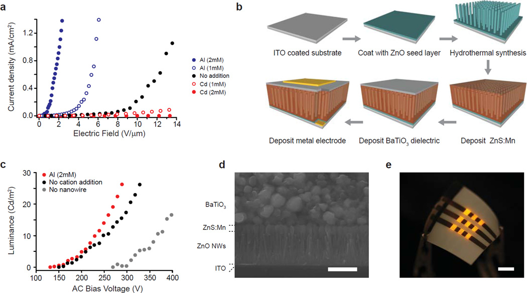
Since the field emission of a nanoneedle scales as ~d/r (where d is nanowire length and r is the apex radius) by Fowler-Nordheim equations26, we exploit the above synthesized nanostructures as a field-emission source. Field-emission of ZnO NWs was greatly enhanced by the addition of aluminum sulfate into the growth solution (Fig. 3a), with turn-on field values (to reach 10 µA/cm2) improved by a factor > 8-fold over nanowire emitters grown under unmodified conditions (0.45 V/µm with 2 mM Al vs. 3.70 V/µm without). Conversely, field-emission was inhibited by the addition of cadmium. The calculated field enhancement factor β = 2.83 × 10⁴ for nanowires grown in the presence of 2mM aluminum sulfate (aspect ratio = 103) vs. β = 2.08 × 10³ without modifiers, was a near 14-fold improvement (Supplementary Fig. S14). These values for turn-on and enhancement rival those reported for VLS-synthesized carbon nanotube emitters (turn-on ~ 0.8 V/ µm, β = 1000 – 35000)27, despite the very low temperature synthesis (<60°C) that is favorable to device integration and in-situ fabrication of polymer-supported nanodevices.
Figure 3. Morphology-coupled field-emission of ZnO nanowires for nanowire-embedded AC electroluminescent devices (NW-ACEL).
(a) Field emission of nanowires grown in the presence of Al (blue), no additional non-zinc ions (black), or Cd (red). Nanoneedles formed in the presence of 2 mM aluminum sulfate had similar emissivity to single wall carbon nanotubes, despite the low temperature synthesis (<60°C). (b) Process flow for a NW-ACEL device, where ZnO NWs enhance field emission to the phosphor from the dielectric. (c) The luminance and efficiency (table S2) of the ACEL device are improved by incorporating the NW-field enhancement layer (black), particularly by high-aspect ratio nanoneedles (red). (d) Cross-sectional scanning electron micrographs of the device. Scale bar = 500 nm (left), 2 um (right). (e) NW-ACEL device fabricated on flexible polyethylene terephthalate (PET). The device was operated at 260 Vrms at 5kHz. Scale Bar = 5 mm.
The combination of low-temperature processing in an aqueous environment and enhanced field emission is ideal for the fabrication of polymer-based, nanowire-embedded AC electroluminescent devices (NW-ACEL) (Fig. 3b–e). In a typical ACEL device, accelerated electrons from the emitter excite dopant atoms in a phosphor, leading to photon emission upon atom relaxation to the ground state. ACEL devices typically have poor efficiency, and thus to improve performance, a NW-ACEL device – with nanoneedles embedded into a ZnS:Mn phosphor layer to enhance field emission from the dielectric ZnO seed layer – was fabricated on flexible, metal-coated polyethylene terepthalate (PET). The yellow/orange electroluminescence (EL) spectrum matched the PL spectrum of the phosphor (Supplementary Fig. S15), indicating that the nanoneedles acted as a field-enhancement layer, as opposed to directly emitting by electron-hole recombination within the semiconductor. The voltage dependent luminance curves (Fig. 3c) show that the enhancement layer lowers the turn-on voltage typically 1.5 – 2X per luminance unit, and improves maximum luminance efficiency by an order of magnitude (Supplementary Table S2).
Furthermore, polymer-compatible low-temperature in-situ syntheses beget possibilities beyond integration onto plastics, such as synthesis in elastomeric microfluidic environments7,28. When nanowires were synthesized in a continuous flow polydimethylsiloxane microreactor, the addition of cadmium and aluminum ions had the same effect on morphology change as in the batch synthesis process (Supplementary Figs. S16 and S17). Synthesis rates were five-fold higher in the microfluidic device vs. in bulk solution because of the constant replenishing of reagents and clearance of homogenous nucleants that consume reactants in solution. Aspect ratios of the structures were effectively unchanged by growth in the microfluidic environment, which supports the notion of improved mass transport being dominant. The nanowire vertical growth rate in the microfluidic device was typically 1.5 – 2 µm/hour vs. 0.3 – 0.4 µm/hour in the optimized batch reactor.
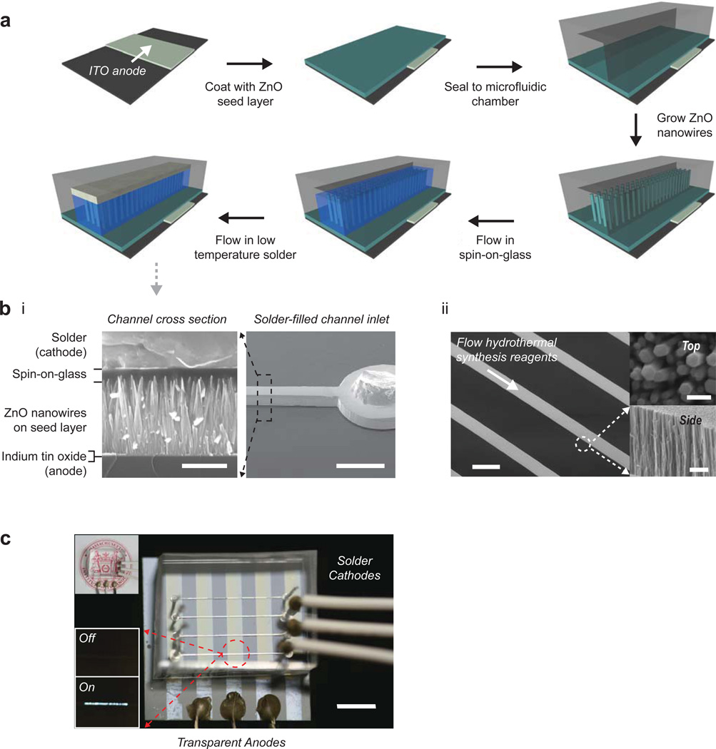
Beyond improved mass transport, hydrothermal synthesis in a microfluidic enables parallel screening of synthesis parameters with minimal reagent consumption (Supplementary Fig. S17). The self-aligned in-situ synthesis and integration into a functional device eliminates the transfer printing or etching steps typically involved in flexible electronics. Microfluidics-based, surface-adherent synthesis offers a route toward simultaneous spatial patterning of functional materials9,29–30. As an example, we demonstrate an all-inorganic in-situ fabricated multi-layer light-emitting diode, by sequentially flowing in solution-processable reagents (Fig. 4). Here, the microfluidic manifold acts not only as a micro-reactor that improves the control over synthesis parameters and vastly diminishes reagent consumption, but also the bottom-up fabrication house of a multi-layer opto-electronic device, and finally, functions as the packaged end-device itself.
Figure 4. In-situ fabrication of an all-inorganic multi-layer opto-electronic device in a microfluidic manifold.
(a) Process flow for the in-situ fabrication of a metal- insulator-semiconductor light-emitting diode (M-I-S LED). The polymeric manifold serves as a micro-reactor, bottom-up fabrication house, and packaged end-device itself. (b) SEM characterization of the device. (i) Cross-section of the complete device. Scale Bar = 500 nm (left), 500 um (right). (ii) Nanowires grown in the microfluidic environment exhibit conformal sidewalls and five-fold increased growth rate (over batch synthesis). Scale Bar = 200 um (left), 500 um (top right), 2 um (bottom right). (c) Transparent M-I-S LED imaged at a partial angle to enhance feature contrast. Top inset depicts transparency of the device at a perpendicular view point. Bottom inset shows emission in the on- and off-states at a forward bias of 10V. Scale Bar = 5 mm.
The metal-insulator-semiconductor light emitting diode (M-I-S LED) was in-situ fabricated by sequentially synthesizing nanowires in a microfluidic manifold on top of indium tin oxide-coated glass or PET, and then by subsequently flowing in an insulating spin-on-glass through the channel, followed by a low melting solder that fills the remainder of the channel8 (Fig. 4a and 4b). The device had an apparent 4V turn-on voltage and a 10−8 A reverse current (or 5 × 10⁻⁶ A/cm2 current density, Supplementary Fig. S18), both indicative of diode function. The fully fabricated and packaged device is optically transparent, as shown in the top inset of Figure 4c, and light emission from an individually addressed pixel in the ON and OFF states are shown in the lower insets (Fig. 4c). The ability to completely in-situ fabricate a multi-layer all-inorganic device with minimal reagent consumption highlights the importance of low-temperature hydrothermal synthesis and improved mechanisms for systematic control.
The chemical system presented here provides a framework for understanding of pH-dependent surface interactions in complex reaction mixtures, upon which one can build further understanding. Our model-based experiments established electrostatics as a dominant control mechanism in low-temperature alkaline hydrothermal synthesis, and further informed the efficient creation of ZnO NW-based devices with enhanced properties and critical features for manufacturing nanostructure-based devices with respect to cost, material integration compatibility, and resource consumption. The synthesis is amenable to processing in microfluidic reactors, begetting multi-layer in-situ synthesis paradigms for spatially complex functional devices. Thus, the development of an electrostatic mechanism to systematically manipulate nanowire aspect ratio may further nanomaterials synthesis chemistry toward the goal of rational control over nanostructure morphology.
METHODS SUMMARY
Single-crystalline nanowires were grown on substrates with zinc oxide seed layers (deposited by sputtering or spin-coating of sol-gels), in aqueous solutions of 10mM zinc sulfate and 0.3M ammonium chloride at pH = 11, 50–60°C. Non-zinc metal sulfates were added to solution prior to growth. All reagents were used as received from Sigma-Aldrich unless noted otherwise; dH2O was 18.2MΩ Millipore water. Alternating current electroluminescent devices were fabricated by first RF sputtering 30 nm-thick seed layers on top of patterned electrodes (by wet-etching of indium tin oxide-coated substrates with aqueous FeCl3/HCl, or thermal evaporation of thin-gold films), synthesizing nanowires to 1.2 um-thickness (in the presence of 2mM aluminum sulfate), RF sputtering of ZnS:Mn phosphor (Kurt J. Lesker), spin-coating of 13 um-thick barium titanate paste as dielectric (Dupont LuxPrint 8153), and deposition of a conductive electrode. Microfluidic devices were fabricated by standard processes, using polydimethylsiloxane (PDMS, Sylgard 184) cast off of molds composed of SU-8 photoresist (Microchem) on silicon wafers, patterned by standard lithographic techniques. The temperature within the microfluidic manifold was controlled with a Peltier stage. The metal-insulator-semiconductor light emitting diode (M-I-S LED) was in-situ fabricated by sequentially synthesizing nanowires in a microfluidic manifold on top of indium tin oxide-coated glass or PET (50°C for 30 minutes at flow rate = 0.6mL/hour), flowing in a spin-on-glass through the channel to a film thickness of 240 nm (200°C for 10 seconds at flow rate = 1mL/hour), followed by a low melting solder that fills the remainder of the channel (In52/Sn48 from AIM Specialty Inc.) at 200°C with low vacuum applied at the fluid outlet8. Thermodynamic calculations were performed in MATLAB. Spectroscopy and metrology were performed with the following: scanning electron microscopy (SEM) (FEI XL30), atomic force microscopy (Digital Instruments Dimension 3000), transmission electron microscopy (JEOL 2010 with energy dispersive x-ray spectroscopy unit (EDS)), x-ray diffractometry (Panalytical X’pert pro), photoluminescence (Hitachi F7000), x-ray photoelectron spectroscopy (PHI 5701 LSci), electroluminescence spectroscopy (Ocean Optics HR2000), photoluminescent spectroscopy (Nanolog fluorescence spectrometer, Horiba Jovin Yvon), luminance measurements (Konica Minolta CS-200), and solid-state device testing (custom built micromanipulator with Keithley 237 high voltage analyzer). During SEM analysis, the diameter was measured at the halfway length along the c-axis of the nanowire.
Supplementary Material
ACKNOWLEDGEMENTS
This research was funded by the Center for Bits and Atoms (NSF CCR0122419) and the MIT Media Lab. We thank Scott Manalis, Vladimir Bulovic, and Angela Belcher for generous use of equipment. The authors acknowledge the partial support of the Korea Foundation for Advanced Studies (awarded to JBJ) and Samsung (research internship to JBJ); the Harvard Society of Fellows (awarded to MP); and the Wallace H. Coulter Early Career Award, NARSAD Young Investigator Award, NSF, and NIH Director's New Innovator Award (awarded to ESB).
Footnotes
AUTHOR CONTRIBUTIONS
JBJ and BYC designed all experiments. JBJ conducted all experiments. BYC assisted with device fabrication, microfluidics, and spectroscopy. MP assisted with microfluidics. All authors contributed to data analysis and writing of the manuscript.
The authors declare no competing financial interests.
REFERENCES
- 1.Vayssieres L. Growth of arrayed nanorods and nanowires of ZnO from aqueous solutions. Adv. Mater. 2003;15:464–466. [Google Scholar]
- 2.Demianets LN, Kostomarov DV, Kuz'mina IP, Pushko SV. Mechanism of growth of ZnO single crystals from hydrothermal alkali solutions. Crystallogra. Rep. 2002;47:S86–S98. [Google Scholar]
- 3.Govender K, Boyle DS, Kenway PB, O'Brien P. Understanding the factors that govern the deposition and morphology of thin films of ZnO from aqueous solution. J. Mater. Chem. 2004;14:2575–2591. [Google Scholar]
- 4.Tian ZRR, et al. Complex and oriented ZnO nanostructures. Nature Mater. 2003;2:821–826. doi: 10.1038/nmat1014. [DOI] [PubMed] [Google Scholar]
- 5.Wagner RS, Ellis WC. Vapor-Liquid-Solid Mechanism of Single Crystal Growth. Appl. Phys. Lett. 1964;4:89–90. [Google Scholar]
- 6.Morales AM, Lieber CM. A laser ablation method for the synthesis of crystalline semiconductor nanowires. Science. 1998;279:208–211. doi: 10.1126/science.279.5348.208. [DOI] [PubMed] [Google Scholar]
- 7.Song YJ, Hormes J, Kumar C. Microfluidic synthesis of nanomaterials. Small. 2008;4:698–711. doi: 10.1002/smll.200701029. [DOI] [PubMed] [Google Scholar]
- 8.Siegel AC, Bruzewicz DA, Weibel DB, Whitesides GM. Microsolidics: Fabrication of Three-Dimensional Metallic Microstructures in Poly(dimethylsiloxane) Adv. Mater. 2007;19:727–733. [Google Scholar]
- 9.Lee SH, et al. Control of the ZnO nanowires nucleation site using microfluic channels. J. Phys. Chem. B. 2006;110:3856–3859. doi: 10.1021/jp056915n. [DOI] [PubMed] [Google Scholar]
- 10.Lincot D. Solution growth of functional zinc oxide films and nanostructures. MRS Bull. 2010;35:778–789. [Google Scholar]
- 11.Richardson JJ, Lange FF. Controlling Low Temperature Aqueous Synthesis of ZnO. 1. Thermodynamic Analysis. Cryst. Growth Des. 2009;9:2570–2575. [Google Scholar]
- 12.Greene LE, Yuhas BD, Law M, Zitoun D, Yang PD. Solution-grown zinc oxide nanowires. Inorg. Chem. 2006;45:7535–7543. doi: 10.1021/ic0601900. [DOI] [PubMed] [Google Scholar]
- 13.Ju S, et al. Fabrication of fully transparent nanowire transistors for transparent and flexible electronics. Nature Nanotech. 2007;2:378–384. doi: 10.1038/nnano.2007.151. [DOI] [PubMed] [Google Scholar]
- 14.Law M, Greene LE, Johnson JC, Saykally R, Yang PD. Nanowire dye-sensitized solar cells. Nature Mater. 2005;4:455–459. doi: 10.1038/nmat1387. [DOI] [PubMed] [Google Scholar]
- 15.Zhang R, Kerr LL. A simple method for systematically controlling ZnO crystal size and growth orientation. J. Solid State Chem. 2007;180:988–994. [Google Scholar]
- 16.Demianets LN, Kostomarov DV. Mechanism of zinc oxide single crystal growth under hydrothermal conditions. Ann. Chim. Sci. Mat. 2001;26:193–198. [Google Scholar]
- 17.Belghiti HE, Pauporté T, Lincot D. Mechanistic study of ZnO nanorod array electrodeposition. Phys. Status Solidi A. 2008;205:2360–2364. [Google Scholar]
- 18.Kisailus D, Schwenzer B, Gomm J, Weaver JC, Morse DE. Kinetically Controlled Catalytic Formation of Zinc Oxide Thin Films at Low Temperature. J. Am. Chem. Soc. 2006;128:10276–10280. doi: 10.1021/ja062434l. [DOI] [PubMed] [Google Scholar]
- 19.Cha JN, et al. Silicatein filaments and subunits from a marine sponge direct the polymerization of silica and silicones in vitro. Proc. Natl. Acad. Sci. U.S.A. 1999;96:361–365. doi: 10.1073/pnas.96.2.361. [DOI] [PMC free article] [PubMed] [Google Scholar]
- 20.Hammond PT. Recent explorations in electrostatic multilayer thin film assembly. Curr. Opin. Colloid Interface Sci. 1999;4:430–442. [Google Scholar]
- 21.Laudise RA, Kolb ED, Caporaso AJ. Hydrothermal Growth of Large Sound Crystals of Zinc Oxide. J. Am. Ceram. Soc. 1964;47:9–12. [Google Scholar]
- 22.Morin SA, Bierman MJ, Tong J, Jin S. Mechanism and Kinetics of Spontaneous Nanotube Growth Driven by Screw Dislocations. Science. 2010;328:476–480. doi: 10.1126/science.1182977. [DOI] [PubMed] [Google Scholar]
- 23.Li WJ, Shi EW, Zhong WZ, Yin ZW. Growth mechanism and growth habit of oxide crystals. J. Cryst. Growth. 1999;203:186–196. [Google Scholar]
- 24.Dem'yanets LN, Kostomarov DV, Kuz'mina IP. Chemistry and Kinetics of ZnO Growth from Alkaline Hydrothermal Solutions. Inorg. Mater. 2002;38:124–131. [Google Scholar]
- 25.Son DH, Hughes SM, Yin YD, Alivisatos AP. Cation exchange reactions-in ionic nanocrystals. Science. 2004;306:1009–1012. doi: 10.1126/science.1103755. [DOI] [PubMed] [Google Scholar]
- 26.Fowler RH, Nordheim L. Electron Emission in Intense Electric Fields. Proc. R. Soc. London, A. 1928;119:173–181. [Google Scholar]
- 27.Jo SH, et al. Field emission of carbon nanotubes grown on carbon cloth. J. Vac. Sci. Technolol. B. 2005;23:2363–2368. [Google Scholar]
- 28.Chan EM, Mathies RA, Alivisatos AP. Size-controlled growth of CdSe nanocrystals in microfluidic reactors. Nano Lett. 2003;3:199–201. [Google Scholar]
- 29.Yiying W, et al. Inorganic Semiconductor Nanowires: Rational Growth, Assembly, and Novel Properties. Chem. Eur. J. 2002;8:1260–1268. doi: 10.1002/1521-3765(20020315)8:6<1260::aid-chem1260>3.0.co;2-q. [DOI] [PubMed] [Google Scholar]
- 30.Wang J, et al. Electrochemical fabrication of conducting polymer nanowires in an integrated microfluidic system. Chem. Commun. 2006:3075–3077. doi: 10.1039/b604426c. [DOI] [PubMed] [Google Scholar]
Associated Data
This section collects any data citations, data availability statements, or supplementary materials included in this article.


