

Abstract
Lattice mismatch in a bimetallic core-shell nanoparticle will cause strain in the epitaxial shell layer, and if it reaches the critical layer thickness misfit dislocations will appear in order to release the increasing strain. These defects are relevant since they will directly impact the atomic and electronic structures thereby changing the physical and chemical properties of the nanoparticles. Here we report the direct observation and evolution through aberration-corrected scanning transmission electron microscopy of dislocations in AuPd core-shell nanoparticles. Our results show that first Shockley partial dislocations (SPD) combined with stacking faults (SF) appear at the last Pd layer; then, as the shell grows the SPDs and SFs appear at the interface and combine with misfit dislocations, which finally diffuse to the free surfaces due to the alloying of Au into the Pd shell. The critical layer thickness was found to be at least 50% greater than in thin films, confirming that shells growth on nanoparticles can sustain more strain due to the tridimensional nature of the nanoparticles.
1. Introduction
Strain engineering has been used to tailor the energy band-edge properties for enhanced charge carrier transport [1, 2] and photoemission properties [3] in semiconductor heterostructures materials. In catalysis, bimetallic core-shell nanoparticles have raised a lot of interest in different fields due to their enhanced properties compared to their monometallic counterparts [4-6]. The electronic structure of the surface atoms can be tuned by changing of core and shell metals thereby tuning their chemical and physical properties. Core-shell nanoparticles present an ideal system to control the strain of the shell metal by changing the core metal and morphology and the shell thickness. The electronic structure of the surface atom can be tuned by the presence of core and shell metals thereby tuning its chemical and physical properties [7, 8]. Both, epitaxial and non-epitaxial shells have been synthesized for different applications [9-13]; however, epitaxial growth has not been thoroughly investigated in core-shell nanoparticles. Several works have studied the effect of elastic strain in the catalytic activity of metal films [14-17] and core-shell nanoparticles [4, 6, 18-22] as well as a substrate for surface-enhanced Raman scattering [23]. Therefore, it is necessary to study in detail the interface of these heterostructures to understand the growth of the shell and the appearance of defects that will alter the properties of such materials.
Strasser et al. demonstrated the increased reactivity of Pt in dealloyed Pt-Cu nanoparticles for fuel cell applications, which was the difference in lattice between the Pt-Cu core and the Pt shell [4]. Their results showed an optimal compressive strain for the oxygen-reduction reaction, which if tuned properly, would make a very efficient catalyst. Filhol et.al. has shown that the catalytic activity can be enhanced by the presence of 4 monolayers of Pd on NiO(110) because of the local strain present in the top Pd layer [24]. This effect was also observed for Pd layers grown on Au seeds in different reactions [25-28].
Despite the fact that epitaxial Au-Pd growth in films is well understood [29-32], the tridimensionality of the nanoparticles changes the strain distribution in the shell, which will change the behavior of the Pd shell changing the strain-release mechanisms compared to thin films.
In this paper, we report a detailed analysis of the epitaxial growth of Pd on Au truncated-octahedral seeds, mainly composed by large {111} surfaces and small {100} surfaces. Lattice mismatch between Au and Pd is about 4.7%, which will lead to the nucleation of dislocations in order for the Pd layers to continue growing. We varied the Pd shell thickness by changing the Pd precursor volume, resulting in shells from 3 layers thick up to 10 nm thick and observed the evolution of the interface by Cs-corrected scanning transmission electron microscopy (STEM). Our results revealed that the strain release mechanism changes from the formation of Shockley partial dislocations (SPD) and stacking faults (SF) to the introduction of misfit dislocations, which will later disappear by diffusion of Au atoms into the Pd shell. These dislocations accommodate strain in the Pd layer changing the physical and chemical properties of the surface of the nanoparticles, hence, it is important to understand the defects that appear at the nanoscale in order to further control the properties of the nanoparticles.
2. Experimental section
All the reagents used: gold (III) chloride trihydrate (HAuCl4.3H2O), potassium tetrachloropalladate (K2PdCl4), sodium borohydride (NaBH4), L-ascorbic acid (AA, 99 %), hexadecyltrimethylammonium bromide (CTAB) were purchased from Sigma-Aldrich and used as received. Deionized water was used throughout the entire experiment.
2.1 Synthesis of Au nanoparticles
The gold nanoparticles were synthesized by modified seed-mediated growth method with heterogeneous nucleation in two steps [33]. In the first step, 75 mM of CTAB (0.2733 gm) was prepared in 10 ml of water in a conical flask and stirred until it was transparent. Afterwards, HAuCl4 (0.25 mM) was added into this solution and vigorously stirred. An ice-cold NaBH4 (10 mM) was rapidly added to the vigorously stirred solution. The injection of NaBH4 (0.6 mL) produced a brown solution. This solution was slowly stirred and undisturbed for 3 hours at 35 °C. The remaining NaBH4 was completely decomposed during the excess reaction time. The Au seeds were produced with sizes ranging from 3 to 5 nm.
In the second step, the Au seeds were grown to 11 nm. In order to grow Au nanoparticles, 2 mL of the above solution were diluted with 50 mL of water. In a separate flask, HAuCl4 (10 mM, 0.1 mL), CTAB (0.2 M, 2 mL) and AA (0.1 M, 1.5 mL) were prepared and diluted in 25 ml of water. Into this 27 mL solution, 2 mL of the seed hydrosol solution was added. The mixture was shaken and slowly stirred. This solution was continuously heated at 35 °C for 8 hours. The solution turned pale purple indicating the formation of 11 nm sized Au nanoparticles.
2.2 Preparation of Au-Pd core-shell nanostructures
The core-shell Au-Pd nanostructures were obtained by adding different volumes of K2PdCl4 (10 mM) to a certain volume of Au nanoparticles (5 mL) and reducing by a weak reducing agent (AA) at 35 °C. Different volumes (10 μL, 20 μL, 40 μL, 75 μL, and 1 mL) of K2PdCl4 (10 mM) were added to the solution containing Au seed (5 mL) at 35 °C. The reaction mixture was reduced using AA (0.1 M, 0.5 mL) and stirred for 6 hours. The color of the solution changed from purple to brown indicating the formation of Au-Pd core-shell nanoparticles. Solution was washed and drop-casted onto a holey carbon Cu grid.
2.3 Electron microscopy characterization
The samples were prepared by placing 3-4 drops of colloidal nanoparticles in water on a carbon film coated Cu grid (3 mm, 300 mesh) and dried under room temperature. The transmission electron microscopy (TEM) images, selected area electron diffraction (SAED) and dark field (DF) images were obtained in a JEOL 2010-F operated at 200 kV. The STEM images were recorded in a probe Cs-corrected JEOL JEM-ARM 200F operated at 200 kV. High angle annular dark field STEM (HAADF) images were obtained with a convergence angle of 26 mrad and the collection semi-angles from 50 to 180 mrad. The probe size used was about 0.09 nm with a probe current of 22 pA. In addition, bright field (BF) STEM images were recorded by using a collection semi-angle of 11 mrad. Energy dispersive x-ray spectroscopy (EDS) spectra were obtained using a probe size of 0.13 nm with the probe current 86 pA.
3. Results and discussion
Our syntheses yielded in average 80% of nanocubes and 20% triangular shapes; however, here we will focus on the evolution of the AuPd interface in the concave nanocubes; then were further characterized by Cs-corrected STEM characterization at several volumes of Pd to observe the progressive growth of the shell and observe strain release mechanisms.
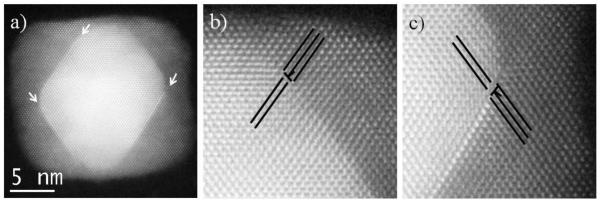
Figure 1a shows a AuPd core-shell nanoparticle (10 μL fo Pd precursor) along a [011] zone axis where it is barely possible to observe the Pd layers grown on the {001} surfaces; however, in Fig. 1b it is easily observed that Pd grows preferentially on Au(111) surfaces. At this stage we can observe that each Au(111) surface has a Pd shell of 3 to 6 layers, but more importantly, all of them present SFs in the Pd layer. The burgers vector of SPDs (a/6<112>) lies in {111} planes; therefore, the formation of SPDs is a good mechanism to release the strain due to the lattice mismatch. However, this is observed at the top {111} Pd layers and not at the interface as seen in other works [29]. Moreover, the creation of a SF in the fcc sequence in the Pd shell does not add a significant amount of extra energy, thereby, the compensation of strain release is larger than the increment of energy to the overall system [30]. Interestingly, SPDs appeared in both, the thickest and the thinner, 6 and 3 Pd layers shells, which has also been observed also for Pd monolayers on Au truncated octahedral nanoparticles [29]. This shows that the formation of SPDs combined with SFs at the surface (not at the interface) for a few Pd layers on Au(111) is the predominant strain-release mechanism to stabilize the nanoparticles. However, we observe a change after the Pd shell is grown a few layers more.
Figure 1.

HAADF STEM images of a core-shell nanoparticles (10 μL of Pd) in a [100] (a) and a [110] zone axes. In a) only 1 or 2 Pd layers on the {100} surfaces can be observed, whereas in b) fully grown Pd(111) surfaces are easily observed. Also magnified images of the for surfaces in b) are shown (S1-4).
Figure 2 shows HAADF images with atomic resolution where it is possible to observe a half grown core-shell nanocube (20 μL of Pd precursor) in a [110] zone axis. This particular nanoparticle is very interesting since it shows four (111) facets with different Pd thicknesses. The inset in Figure 2a shows a magnified image of the lower left corner of the nanocube revealing a Pd thickness of 6 layers, with a SF at the surface. This is consistent with our previous observation. However, the other 3 corners present 15 (top left), 15 (top right) and 13 (bottom right) Pd layers, at the same time that more defects are observed in all 3 of them. Starting from the top left corner (Fig. 2b), we can observe several defects at this interface. First, a misfit dislocation is apparent at the interface (marked by the “T” and the black lines), which is combined with a SPD and a SF in the dislocation plane (marked by closed arrow) all the way to the surface, then the Pd shell follows the ABC sequence, until it reaches the outer layer, which changes in stacking sequence again and presents a SF (marked by open arrow). This shows the complexity of strain-release mechanisms as the Pd layers grow on the Au nanoparticle. Different kinds of defects are introduced in order to compensate the lattice mismatch. This misfit dislocation is a pure edge dislocation with a Burgers vector a/2<110>. On the top right corner (Fig. 2c), we can observe that there is a misfit dislocation (marked by the inverted “T”) but no other defects were observed. While this interface has 15 Pd layers, the same as the top left corner, the concentration of defects is very different.
Figure 2.

a-d) HAADF STEM images of a core-shell nanoparticles from a the 20 μL of Pd synthesis. Inset in a) shows a magnified image of the bottom left corner of the nanocube in a).
From Fig. 2a it is possible to observe that the top right Au(111) plane is significantly smaller than the top left Au(111) plane; therefore, the amount of strain accumulated in the top right corner is much less then the top left, allowing the misfit dislocation to release enough strain to stabilize the interface. Finally, the bottom right corner (Fig. 2d) present a SPD (marked by the black inverted “T”) combined with a SF (marked by an arrow), but also presents misfit dislocation near the surface (marked by the white inverted “T”). While this last corner only presents 13 Pd layers, the size of the Au(111) surface is bigger than the top right, which probably has more strain built up, which in turn caused the creation of the SPD and the SF. Interestingly, the misfit dislocation is interacting with the SF at the interface, in a similar way as in the top left corner, which means that the creation of one most likely will cause the other to appear; however, the top right corner contradicts this since no SPD is observed at first sight. By examining closely the HAADF and BF (not shown) STEM images of the top right corner, there is a diffusive signal between the atomic columns, which might indicate atoms in a different position from the fcc arrangement, meaning that a SPD and a small SF might exist, but is blurred due to the intensity of all the other atoms and cannot be determined with certainty.
These results show that the critical thickness for Pd grown on Au(111) surfaces of nanoparticles is between 6 and 13 Pd(111) layers (i.e. between 1.108 nm and 2.571 nm). This result differs from what was found before in Pd(111) surfaces deposited on Au(111) surfaces in thin films. Critical layer thicknesses of 2 [34] and 4 [35] layers were observed on epitaxilly grown Pd(111) surfaces on Au(111) films. The difference is quite substantial, evidencing that the 3D nature of the core-shell nanoparticles plays an important role in the strain distribution during the shell growth.
After the core-shell nanoparticles acquired a cubic shape no more SPDs nor SFs are observed at the outer Pd layer, mostly due to the reduction in size of the Pd(111) planes after they grow; however, defects are still observed at the interface. Figure 3a shows a fully formed nanocube 18 nm in size (40 μL of Pd precursor synthesis) where defects can be observed (marked by arrows). Fourier analysis revealed two misfit dislocations on the right top and bottom corners (Fig. 3b-c), while no extra planes appeared in the left corners. From Fig. 3b and c we can observe that the atomic columns in the nanoparticle are distorted near the defects (compared to the top part of the nanocube), which means that there should be atoms in positions different from the usual fcc structure, blurring and distorting the intensity profile. This is also observable on the left corners where no misfit dislocation nor SF were found, meaning that some defects exist in those interfaces but due to the small number of atoms in the defect, it is not possible to accurately identify them.
Figure 3.
a-c) HAADF STEM images of a nanocube from the 40 μL of Pd synthesis.
The analysis of a 20 nm (Fig. 4) nanocube resulted in very similar results, a SPDs and a SF interacting with a misfit dislocation was found in one corner (top right) (Fig. 4d); however, this was not the same for the other corners. On the top left corner a SPD and a SF were found at the interface but no misfit dislocation was readily distinguishable. Moreover, a considerable amount of lattice distortion was observed at the interfaces, as shown in Fig. 4c. This distortion can either be caused by the Pd layer relaxation or may be the result of defects that are not edge-on in this zone axis. The tridimensionality of the nanoparticle starts to play an important role in the stability of the interface, but more importantly, in the observation of them. It is not possible to be completely certain if there are more defects or not from this projection, nonetheless, valuable information was gained from the observed interfaces.
Figure 4.

a-d) HAADF STEM images of a nanocube from the 75 μL of Pd synthesis
After growing the Pd layer even more (about 10 nm) the nanocubes resulted in a 30 nm mean size (1 mL of Pd precursor). Interestingly, most of these nanocubes did not present any defects in their structure. Figure 5a shows a HAADF image with atomic resolution of the core of a 30 nm nanocube where no dislocations are observed, and also, no significant lattice distortion is noticeable. On the other hand, we did observe a defect but at the Pd shell of a nanocube of this size. Figure 5b shows a BF image of a nanocube with a double SPD bounded by a double SF in the shell, while Fig. 5c and d show magnified HAADF images of the big and small squares in b respectively. In Fig. 5c it can be seen that two Pd(111) planes present distorted atomic columns, while in Fig. 5d confirms that the SFs does not reach the surfaces. Remarkably, no misfit dislocations were observed even at these sizes. Ding et al. [29] observed something similar in their results; they attributed this effect to the diffusion of Au into the Pd shell. The diffusion of Au atoms into the Pd shell will change the lattice constant of Pd decreasing the accumulated strain at the interface, moving the defects all the way to the free surfaces that could have been formed during the shell growth [36]. This is understandable since it has been shown that Au and Pd form a nearly ideal miscible alloy at all compositions [31]. Density functional theory calculations showed that intermixing in a (100) AuPd interface is energetically favorable [30]; which we can correlate with our observations. Pd grows preferentially on (111) surfaces, and by the time the nanocube is formed, only a few Pd layers are grown on the (100) surfaces, therefore, a bigger shell is necessary in order to increase the number of Pd layers on the Au(100) surfaces to promote the alloying of the shell, which in turn will reduce the strain and will erase existing dislocations. In addition, the surface free energy for Au (1.63 J/m2) is lower than that of Pd (2.04 J/m2) which drives the Au atoms to go to the Pd shell, forming an alloy structure in the shell [37]. This was confirmed experimentally by a 2D EDS map of a nanocube, shown in Figure 6.
Figure 5.

a-d) HAADF STEM images of nanocubes from the 1 mL of Pd synthesis.
Figure 6.
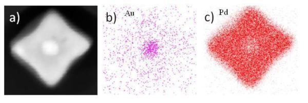
EDS mapping of a nanocube from the 1 mL of Pd synthesis. a) shows the HAADF image of the nanocube, while b) and d) show the Au-L and Pd-L signals respectively.
4. Conclusions
Our experimental results revealed new insights on the formation of AuPd core-shell nanoparticles. Some works have shown experimental results on the structure of core-shell nanoparticles; however, their observations were limited and did not follow any trends in these structures [10, 32, 38, 39]. Here we show the strain release mechanisms that take place as a Pd shell grows over a Au nanoparticle. SPDs and SFs at the Pd surfaces are the first mechanism to release lattice mismatch strain up to 6 Pd layers (1.108 nm). At 13 Pd layers (2.528 nm) the mechanism changes, SPDs and SFs appear at the interface along with misfit dislocations. We could not determine which of these two defects appear first, but most likely the creation of one of them causes the nucleation of the second one to further decrease the lattice mismatch. Finally, when the Pd layer is about 10 nm no defects are observed at the interface, but at the Pd shell, which is caused by the diffusion of Au atoms into the Pd shell, reducing the lattice mismatch and previously existent defects. This shows that inter diffusion plays an important role in the epitaxial growth of core-shell nanoparticles. The critical layer thickness was found to be at least 50% more than that for films. This shows that larger pseudo morphical shells can be grown on nanoparticles than in thin films. Our results provide valuable data about the strain release mechanism of core-shell nanoparticles that will help others take a step further in the controlled synthesis of this type of nanoparticles.
Highlights.
Au-Pd core-shell nanocube and pseudo-triangular plate (PTP) were synthesized using modified seed mediated growth process.
Aberration corrected scanning transmission electron microscopy was used to study the atomic resolution of the nanostructures.
Both the structures present high index facet surfaces.
Two structural defects were found. Shockley partial dislocation bounded by a double stacking fault is observed on <011> zone axis in nanocube while the twinning along [111] is present in PTP.
Diffraction contrast images and electron diffraction were used to characterize the structures, structural defects and strain fields.
Acknowledgements
This work was supported This project was supported by grants from the National Center for Research Resources (5 G12RR013646-12) and the National Institute on Minority Health and Health Disparities (G12MD007591) from the National Institutes of Health The authors would like to acknowledge to the NSF for support with grants DMR-1103730, “Alloys at the Nanoscale: The Case of Nanoparticles Second Phase and PREM: NSF PREM Grant # DMR 0934218; “Oxide and Metal Nanoparticles- The Interface Between Life Sciences and Physical Sciences”
Footnotes
Publisher's Disclaimer: This is a PDF file of an unedited manuscript that has been accepted for publication. As a service to our customers we are providing this early version of the manuscript. The manuscript will undergo copyediting, typesetting, and review of the resulting proof before it is published in its final citable form. Please note that during the production process errors may be discovered which could affect the content, and all legal disclaimers that apply to the journal pertain.
References
- 1.Lee ML, et al. Strained Si, SiGe, and Ge channels for high-mobility metal-oxide-semiconductor field-effect transistors. Journal of Applied Physics. 2005;97(1):011101–28. [Google Scholar]
- 2.Nainani A, et al. Engineering of strained III–V heterostructures for high hole mobility. Electron Devices Meeting (IEDM), 2009 IEEE International.2009. [Google Scholar]
- 3.Sun X, et al. Room-temperature direct bandgap electroluminesence from Ge-on-Si light-emitting diodes. Opt. Lett. 2009;34(8):1198–1200. doi: 10.1364/ol.34.001198. [DOI] [PubMed] [Google Scholar]
- 4.Strasser P, et al. Lattice-strain control of the activity in dealloyed core–shell fuel cell catalysts. Nat Chem. 2010;2(6):454–460. doi: 10.1038/nchem.623. [DOI] [PubMed] [Google Scholar]
- 5.Edwards JK, et al. Direct synthesis of hydrogen peroxide from H2 and O2 using Au-Pd/Fe2O3 catalysts. Journal of Materials Chemistry. 2005;15(43):4595–4600. [Google Scholar]
- 6.Montes de Oca MG, et al. Electrocatalytic Properties of Strained Pd Nanoshells at Au Nanostructures: CO and HCOOH Oxidation. The Journal of Physical Chemistry C. 2011;116(1):692–699. [Google Scholar]
- 7.Rodriguez JA, Goodman DW. The Nature of the Metal-Metal Bond in Bimetallic Surfaces. Science. 1992;257(5072):897–903. doi: 10.1126/science.257.5072.897. [DOI] [PubMed] [Google Scholar]
- 8.Ertl G. Dynamics of reactions at surfaces. In: Bruce HK, Gates C, editors. Advances in Catalysis. Academic Press; 2000. pp. 1–69. [Google Scholar]
- 9.Zhang J, et al. Nonepitaxial Growth of Hybrid Core-Shell Nanostructures with Large Lattice Mismatches. Science. 2010;327(5973):1634–1638. doi: 10.1126/science.1184769. [DOI] [PubMed] [Google Scholar]
- 10.Long NV, et al. New Experimental Evidences of Pt–Pd Bimetallic Nanoparticles with Core–Shell Configuration and Highly Fine-Ordered Nanostructures by High-Resolution Electron Transmission Microscopy. The Journal of Physical Chemistry C. 2012;116(22):12265–12274. [Google Scholar]
- 11.Perillat-Merceroz G, et al. Strain relaxation by dislocation glide in ZnO/ZnMgO core-shell nanowires. Applied Physics Letters. 2012;100(17):173102–4. [Google Scholar]
- 12.Kavanagh KL, et al. Faster radial strain relaxation in InAs--GaAs core--shell heterowires. Journal of Applied Physics. 2012;111(4):044301–9. [Google Scholar]
- 13.Dayeh SA, et al. Direct Measurement of Coherency Limits for Strain Relaxation in Heteroepitaxial Core/Shell Nanowires. Nano Letters. 2012 doi: 10.1021/nl3022434. [DOI] [PubMed] [Google Scholar]
- 14.Pronkin S, Hara M, Wandlowski T. Electrocatalytic properties of Au(111)-Pd quasi-single-crystal film electrodes as probed by ATR-SEIRAS. Russian Journal of Electrochemistry. 2006;42(11):1177–1192. [Google Scholar]
- 15.Kibler LA, et al. Tuning Reaction Rates by Lateral Strain in a Palladium Monolayer. Angewandte Chemie International Edition. 2005;44(14):2080–2084. doi: 10.1002/anie.200462127. [DOI] [PubMed] [Google Scholar]
- 16.Minniti M, et al. Enhanced selectivity towards O[sub 2] and H[sub 2] dissociation on ultrathin Cu films on Ru(0001) The Journal of Chemical Physics. 2012;137(7):074706–6. doi: 10.1063/1.4746942. [DOI] [PubMed] [Google Scholar]
- 17.Filhol JS, et al. Highly Strained Structure of a Four-Layer Deposit of Pd on Ni(110): A Coupled Theoretical and Experimental Study. Physical Review Letters. 2002;89(14):146106. doi: 10.1103/PhysRevLett.89.146106. [DOI] [PubMed] [Google Scholar]
- 18.Njoki PN, et al. Exploiting core-shell and core-alloy interfaces for asymmetric growth of nanoparticles. Chemical Communications. 2012;48(84):10449–10451. doi: 10.1039/c2cc34184k. [DOI] [PubMed] [Google Scholar]
- 19.Zhong CJ, Maye MM. Core–Shell Assembled Nanoparticles as Catalysts. Advanced Materials. 2001;13(19):1507–1511. [Google Scholar]
- 20.Nilekar AU, et al. Preferential CO Oxidation in Hydrogen: Reactivity of Core–Shell Nanoparticles. Journal of the American Chemical Society. 2010;132(21):7418–7428. doi: 10.1021/ja101108w. [DOI] [PubMed] [Google Scholar]
- 21.Alayoglu S, et al. Ru-Pt core-shell nanoparticles for preferential oxidation of carbon monoxide in hydrogen. Nat Mater. 2008;7(4):333–338. doi: 10.1038/nmat2156. [DOI] [PubMed] [Google Scholar]
- 22.Wintterlin J, et al. Atomic-Scale Evidence for an Enhanced Catalytic Reactivity of Stretched Surfaces. Angewandte Chemie International Edition. 2003;42(25):2850–2853. doi: 10.1002/anie.200250845. [DOI] [PubMed] [Google Scholar]
- 23.Hu J-W, et al. Palladium-Coated Gold Nanoparticles with a Controlled Shell Thickness Used as Surface-Enhanced Raman Scattering Substrate. The Journal of Physical Chemistry C. 2006;111(3):1105–1112. [Google Scholar]
- 24.Sao-Joao S, et al. Structure and Deformations of Pd–Ni Core–Shell Nanoparticles. The Journal of Physical Chemistry B. 2004;109(1):342–347. doi: 10.1021/jp040473i. [DOI] [PubMed] [Google Scholar]
- 25.Zhou W, Lee JY. Highly active core–shell Au@Pd catalyst for formic acid electrooxidation. Electrochemistry Communications. 2007;9(7):1725–1729. [Google Scholar]
- 26.Dimitratos N, et al. Solvent-free oxidation of benzyl alcohol using Au-Pd catalysts prepared by sol immobilisation. Physical Chemistry Chemical Physics. 2009;11(25):5142–5153. doi: 10.1039/b900151b. [DOI] [PubMed] [Google Scholar]
- 27.Kuai L, et al. Au–Pd Alloy and Core–Shell Nanostructures: One-Pot Coreduction Preparation, Formation Mechanism, and Electrochemical Properties. Langmuir. 2012;28(18):7168–7173. doi: 10.1021/la300813z. [DOI] [PubMed] [Google Scholar]
- 28.Chen H, et al. Graphene supported Au-Pd bimetallic nanoparticles with core-shell structures and superior peroxidase-like activities. Journal of Materials Chemistry. 2011;21(44):17658–17661. [Google Scholar]
- 29.Ding Y, et al. Atomic Structure of Au–Pd Bimetallic Alloyed Nanoparticles. Journal of the American Chemical Society. 2010;132(35):12480–12486. doi: 10.1021/ja105614q. [DOI] [PubMed] [Google Scholar]
- 30.Tikare V, et al. First-Principles Calculations of the Atomic and Electronic Structures in Au-Pd Slab Interfaces. Solid State Phenomena. 2008;139:29–34. [Google Scholar]
- 31.Weissman-Wenocur DL, et al. Photoemission study of Au overlayers on Pd(111) and the formation of a Pd-Au(111) alloy surface. Physical Review B. 1983;27(6):3308–3317. [Google Scholar]
- 32.Akita T, et al. Analytical TEM observation of Au–Pd nanoparticles prepared by sonochemical method. Catalysis Today. 2008;131(1–4):90–97. [Google Scholar]
- 33.Fan F-R, et al. Epitaxial Growth of Heterogeneous Metal Nanocrystals: From Gold Nano-octahedra to Palladium and Silver Nanocubes. Journal of the American Chemical Society. 2008;130(22):6949–6951. doi: 10.1021/ja801566d. [DOI] [PubMed] [Google Scholar]
- 34.Cherns D, Stowell MJ. Misfit dislocation sources in epitaxial films part II: Growth of Pd on (111) Au substrates. Thin Solid Films. 1975;29(1):127–143. [Google Scholar]
- 35.Kibler LA, et al. Initial stages of Pd deposition on Au(hkl) Part I: Pd on Au(111) Surface Science. 1999;443(1–2):19–30. [Google Scholar]
- 36.van der Merwe JH, Woltersdorf J, Jesser WA. Low energy dislocation structures in epitaxy. Materials Science and Engineering. 1986;81:1–33. (0) [Google Scholar]
- 37.Mezey LZ, Giber J. The Surface Free Energies of Solid Chemical Elements: Calculation from Internal Free Enthalpies of Atomization. Japanese Journal of Applied Physics. 1982;21:1569. (Copyright (C) 1982 Publication Board, Japanese Journal of Applied Physics) [Google Scholar]
- 38.Taguchi N, et al. Study of Au–Pd core–shell nanoparticles by using slow positron beam. Applied Surface Science. 2008;255(1):164–166. [Google Scholar]
- 39.Ding Y, et al. Misfit dislocations in multimetallic core-shelled nanoparticles. Applied Physics Letters. 2012;100(11):111603–4. [Google Scholar]