

Abstract
We have developed a novel 4-channel prototype stimulation circuit for implantable neurological stimulators (INS). This Switched-Capacitor based Stimulator (SCS) aims to utilize charge storage and charge injection techniques to take advantage of both the efficiency of conventional voltage-controlled stimulators (VCS) and the safety and controllability of current-controlled stimulators (CCS). The discrete SCS prototype offers fine control over stimulation parameters such as voltage, current, pulse width, frequency, and active electrode channel via a LabVIEW graphical user interface (GUI) when connected to a PC through USB. Furthermore, the prototype utilizes a floating current sensor to provide charge-balanced biphasic stimulation and ensure safety. The stimulator was analyzed using an electrode-electrolyte interface (EEI) model as well as with a pair of pacing electrodes in saline. The primary motivation of this research is to test the feasibility and functionality of a safe, effective, and power-efficient switched-capacitor based stimulator for use in Deep Brain Stimulation.
I. Introduction
Integrated medical stimulators have been around for almost six decades, beginning with the development of the implantable cardiac pacemaker and gaining momentum with the miniaturization of integrated circuit technologies [1]. Year by year, devices are becoming smaller, more accurate, and more capable while consuming less power. Such advances in technology have allowed engineers and physicians to push the state of art and utilize implantable neurostimulators to treat deafness, pain, blindness, Parkinson’s and numerous other illnesses [2]. To ensure wide acceptance of these new treatments, it is essential that these devices be designed to be minimally invasive, safe, and extensively autonomous. As a result, wireless power and efficient stimulation techniques have been popular topics of research [3].
As the field of medical devices has grown, many new techniques and therapies using electrical stimulation have come to the forefront of research. Namely, Deep Brain Stimulation (DBS), which has recently been proven as an effective therapy for treating Parkinson’s disease, Essential Tremor and Dystonia, is a therapy in need of miniaturization and sophisticated stimulation techniques [4]. Current DBS implants consist of a battery powered device, implanted under the skin in the chest area, with four leads that run across the neck to reach electrodes that are implanted in the inner regions of the brain from the top of the head. By eliminating the implanted battery and reducing the number of components, DBS has the potential of reaching wide spread acceptance among physicians and patients, alike [2].
Typically, neural stimulation is accomplished via voltage controlled stimulation (VCS) or current controlled stimulation (CCS). While VCS has been proven to be very efficient, ensuring charge balanced operation is complex due to time and position varying tissue impedances among other issues. Charge balancing refers to maintaining a net charge of zero at a stimulation site. If charge is not appropriately nullified, a build-up of charge at the active site will result in a potential difference at the electrode-electrolyte interface (EEI). If this difference exceeds the safe limit, known as the water window, electrolysis of extracellular fluid could lead to both tissue and electrode damage [5].
Conversely, CCS is much safer, providing more control over charge injection. In fact, numerous topologies have been developed and proposed that eliminate current mismatches with very fine resolution. However, CCS devices boast much lower efficiencies due to the output voltage necessary to drive predetermined current through variable electrode and tissue impedances.
A Switched-Capacitor based Stimulator (SCS) can, potentially, find a point at which the safety, simplicity, and efficiency can be optimized while replacing the existing bulky solution with a smaller localized implementation. Capacitive stimulation is a new area of interest that was first investigated by Kelly and Wyatt in [3], who showed that incrementally increasing and decreasing stimulation voltage can reduce the power consumption per electrode by 53% when compared to aggressive CCS techniques. Similarly, in [6], the authors compared the characteristics of VCS, CCS, and SCS systems. They showed that if implemented with similar topologies, a VCS, CCS, and SCS stimulator can achieve power conversion efficiencies of 92, 65, and 77%, respectively. Finally, in [7] and [8] an inductively powered, high efficiency CMOS rectifier was utilized to implement an SCS topology capable of charging dual 1 μF capacitors to ±1.9V (from an induced 2.5V sinusoidal input) in 120 μs at 78% efficiency.
Based on the conclusions of these works, it was the intention of this research to further develop a discrete SCS system using efficient voltage converter techniques to provide flexible output voltages and charge-balanced operation. Prototype measurements are essential in this case since simulations are not very effective due to the complexities of the electrode-electrolyte interface, which vary significantly with electrode type, stimulation environments, type of tissue, and stimulus waveforms. Eventually, such a system can be miniaturized by integration and used to explore the efficacy of capacitive stimulation via in-vitro and in-vivo experiments to further verify the effectiveness of exponential stimulation patterns [9].
II. Stimulator Architecture
The system block diagram of the proposed SCS prototype is shown in Fig. 1. The integrated version will be powered by an inductive link with a power management front end. But in the current version (see Fig. 3), the front end of the system is a commercial capacitor charger IC (LT3484, Linear Technology, Milpitas, CA) that consists of an isolated flyback converter and external step-up transformer capable of generating output voltages up to 350 V from a battery voltage as low as 2.5 V. Since safe stimulation voltages are typically less than 10 V, we added a sensing feedback network to limit the output voltage to 10 V.
Fig. 1.
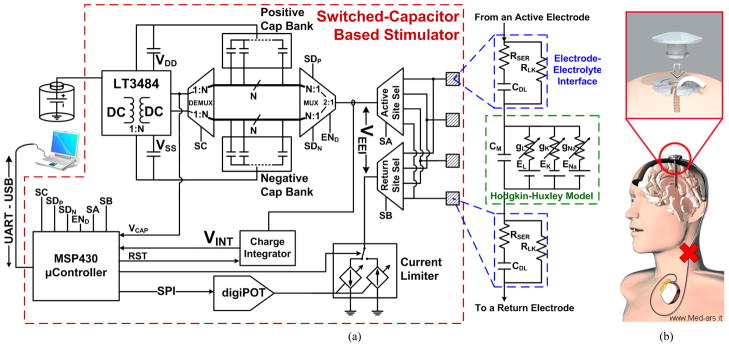
(a) Block diagram of the switched-capacitor based stimulator (SCS), which has been implemented as a discrete circuit. (b) The concept of a head-mounted DBS, which eliminates the pulse generator in the chest area and subcutaneous wire passing across the skin.
Fig. 3.
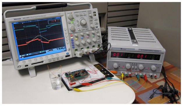
SCS measurement setup with cardiac electrodes in saline solution.
Dedicated banks of positively charged and negatively charged capacitors can be multiplexed for simultaneous charging and biphasic (anodic then cathodic) discharging. Four 1 μF storage capacitors per bank were used in this prototype to cyclically charge and discharge as necessary. Stimulation path can be selected from four stimulation sites; one active electrode, which will deliver the stimulus charge, and one return electrode, which will shape and guide the stimulus current to ground. Furthermore, to provide feedback control over stimulus pulses, a floating current sensor monitors the stimulation current, which is then integrated and compared to a near zero reference voltage. When the amount of charge injected and withdrawn is equivalent, the stimulation cycle is stopped and very little residual charge is left at the stimulation site.
A graphical user interface (GUI), shown in Fig. 3, was developed in LabVIEW to provide user programmability over key system parameters, such as stimulation voltage (VCAP) and current limits (LimP/LimN), stimulation pulse width (TP/TW/TN) and frequency (PPD), stimulation site selection (ESel), and charging/stimulation enable signals (VCH/StimEN). These parameters are then transmitted to an onboard MSP430 microcontroller (Texas Instruments, Dallas, TX) via a USB to UART connector, where the data is deciphered, successful transmission is verified, and the stimulation commands are executed.
A. Capacitor Charging Front End
The capacitor charging front end consists of a commercial flyback DC/DC converter specially designed for charging capacitive loads. The energy efficiency of the LT3484 is dependent on a number of factors, including output voltage, series resistance, and average input current. Since the desired output voltage was an order of magnitude lower than the manufacturer suggested value, it was important to adjust the other factors to ensure nominal energy efficiency. It was also important to utilize fast switches and diodes to reduce the reverse recovery time and reverse current losses, which can further degrade energy efficiency.
To control charging, the MSP430 provides an enable signal to the capacitor charger. During a charging interval, the microcontroller monitors a fraction of the output voltage, digitizing and comparing that value to the value, VCAP, received from the GUI. Once the desired output voltage is reached, charging is disabled and the next capacitor is switched in to begin charging. The system cyclically charges all capacitors in the bank until all of them are charged.
B. Capacitive Stimulator
Stimulation is also controlled via the GUI, providing user programmability to the various parameters shown in Fig. 3a. Programmability is a crucial requirement in research and development stage stimulators to provide a platform for complete analysis of various parameters as well as flexibility in treatment options. Once programmed, the microcontroller can autonomously perform the desired stimulation until a command is sent for the system to be reprogrammed.
During a stimulation period, the anodic phase connects a positively charged capacitor to the active electrode. Charge is injected into the tissue and returns through a second electrode into a current limiting MOSFET. By controlling the gate voltage of this FET, the user can define a positive current limit that will pass through the target tissue. The gate voltage of the FET is set by the microcontroller and generated by a digital potentiometer (AD5292, Analog Devices, Norwood, MA), providing stimulus currents of ±5 mA with gate voltages of ±2.5 V. If the stimulating current is too high, often at the beginning of an exponentially decaying stimulus waveform, the FET operates in the saturation region and acts as a current sink. However, as the capacitor voltage decreases, the FET drifts into the triode region where it will allow an exponential decay in the stimulation current. Similarly, for the cathodic phase, the negatively charged capacitor is connected to the active electrode and current is limited in the same way. Two benefits arise from current limiting the stimulation pulse. First, it reduces the high frequency, high amplitude stimulation components that have been shown to potentially damage the tissue and electrode [10]. Second, it reduces the slew rate requirements for measuring the stimulation current accurately.
C. Closed-Loop Charge Balancing
As mentioned before, a safe stimulator must be able to nullify charge at the EEI to ensure the system can be used for a long time without damaging the tissue or electrode. Numerous charge-balancing techniques have been proposed in the past, most of which are only applicable to current stimulation [11]. The approach taken here is to monitor and integrate the stimulation current via a floating current sense resistor, programmable gain amplifier, and opamp in an integrator configuration (see Fig. 1). During the cathodic phase, the integrated current value is compared to a near zero reference voltage using a comparator. Once the integrated value reaches zero, the cathodic stimulation is ceased with a residual charge of zero at the tissue interface. Due to voltage offsets and jitter, this method is not failsafe. However, based on our measurements, the average residual voltage was only ~10 mV.
III. Efficiency Analysis
The key parameter of concern in this work is the energy efficiency (ηE) of the stimulator. For this prototype, input energy (EIN) is the integration of power over time, which can be broken down as the product of the battery voltage (VDC), average input current (IAVG) and charging time (tCH),
| (1) |
The output energy (EOUT) is readily derived from the positive and negative capacitance values (CP, CN) and output voltages (VP, VN) of the storage capacitors according to,
| (2) |
Dividing EIN/EOUT gives the power efficiency of the system, assuming that CP = CN = CL and VP = VN = VL,
| (3) |
It is important to note that (3) provides a clear relationship between the stimulator efficiency and the output voltage, input voltage, and input current.
IV. Simulation and Measurement Results
Measurements were taken using the EEI circuit model, shown in Fig. 1, and stainless steel cardiac electrodes in buffered saline solution, as shown in Fig. 3. Electrodes were a pair of Keith needles from a temporary cardiac pacing wire set (A&E Medical, Farmingdale, NJ), which were placed 85 mm apart with approximately 72 mm2 of immersed surface area. Circuit component values in the model are dependent on the chosen electrode and electrolyte, but typical values for the double layer capacitance and its series resistance are 0.3~3 μF and 1.1~2.5 kΩ, respectively [3]. The values we chose for our measurements were 980 nF and 1.15 kΩ in series, plus a 5 MΩ leakage resistance in parallel. The measured capacitance and resistance between the electrodes in saline solution were 1.025 μF and 314Ω, respectively.
Figs. 4a and 4b show the biphasic-bipolar stimulation waveforms in the circuit and saline solution, respectively, when VCAP = 10 V, LimP/LimN = 1 mA, TP/TW/TN = 1/0.1/4 ms, and PPD = 10 ms. The measured EEI voltage, VEEI (red) (see Fig. 1a), was measured in both cases by differentially probing the voltage across the active and return electrodes. These waveforms also show the charge integrator output voltage, VINT (blue). In addition, the stimulator output voltage, VSTIM, and the stimulus current, ISTIM, waveforms are shown.
Fig. 4.

Stimulation measurements with (a) electrode-electrolyte interface model - VEEI (red), VINT (blue), VSTIM (teal), ISTIM (green) - and (b) electrode pair in saline - VEEI (red), VINT (blue), VSTIM (orange), ISTIM (purple).
It can be seen in both cases that the system can effectively apply the stimulation parameters, control the stimulation current limits, and ensure charge balancing at the sites by returning VSTIM back to zero. These particular waveforms, however, are not showing the exponentially decaying current because the current limits and duration are relatively small. The present prototype achieved a maximum power efficiency of 58.8% with an output voltage of ±11.4 V.
V. Conclusion
We have developed a prototype switched-capacitor based stimulator for studying this group of stimulators and collecting data for the implementation of a highly efficient head-mounted deep brain stimulator. The functionality of the circuit and feasibility of SCS operation have been verified using a battery powered commercial front-end. A power efficiency of 58.8% was achieved at a stimulation voltage of 11.4 V and the effectiveness of current limiting safety feature was demonstrated. We have also designed a GUI for versatile control of the stimulation parameters. While the efficacy of exponentially decaying stimulus pulses have yet to be tested [12], this prototype may be useful in characterizing the effects of such stimuli in various in vitro and in vivo experiments.
Fig. 2.

Visualizing the stimulus waveform (a) of the SCS system based on the user defined stimulation parameters that are adjusted through a GUI (b) in the LabVIEW environment.
Acknowledgments
This work was supported in part by Texas Instruments Inc.
Contributor Information
Jose Vidal, Jr., Email: jose.vidal@gatech.edu, Electrical and Computer Engineering Department, Georgia Institute of Technology, Atlanta, GA 30308 USA (phone: 256-627-1123).
Maysam Ghovanloo, Email: mgh@gatech.edu, Electrical and Computer Engineering Department, Georgia Institute of Technology, Atlanta, GA 30308 USA.
References
- 1.Haddad SAP, Houben RPM, Serdijin WA. The evolution of pacemakers. IEEE Eng in Med and Bio Magazine. 2006 May-Jun;25(3):38–48. doi: 10.1109/memb.2006.1636350. [DOI] [PubMed] [Google Scholar]
- 2.Krames ES, Peckham PH, Rezai AR, editors. Neuromodulation. Oxford: Elsevier Ltd; 2009. [Google Scholar]
- 3.Kelly SK, Wyatt J. A power-efficient voltage-based neural tissue stimulator with energy recovery. IEEE Digest Intl Solid-State Cir Conf. 2004 Feb;:228–524. [Google Scholar]
- 4.Jensen S, Molnar G, Giftakis J, Santa W, Jensen R, Carlson D, Lent M, Denison T. Information, energy, and entropy: Design principles for adaptive, therapeutic modulation of neural circuits. European Solid-State Cir Conf. 2008 Sep;:32–39. [Google Scholar]
- 5.Merrill DR, Bikson M, Jefferys JGR. Electrical stimulation of excitable tissue: design of efficacious and safe protocols. J Neuroscience Methods. 2005 Feb;141:171–198. doi: 10.1016/j.jneumeth.2004.10.020. [DOI] [PubMed] [Google Scholar]
- 6.Simpson J, Ghovanloo M. An Experimental Study of Voltage, Current, and Charge Controlled Stimulation Front-End Circuitry. Proc IEEE Int’l Symp on Cir and Sys. 2007 May;:325–328. [Google Scholar]
- 7.Bawa G. MS Thesis. Department of Electrical Engineering, North Carolina State University; Raleigh: Jul, 2008. A switched capacitor based micro-stimulator for deep brain stimulation. [Google Scholar]
- 8.Bawa G, Ghovanloo M. Active high power conversion efficiency rectifier with built-in dual-mode back telemetry in standard CMOS technology. IEEE Trans Biomed on Cir and Syst. 2008 Sep;2(3):184–192. doi: 10.1109/TBCAS.2008.924444. [DOI] [PubMed] [Google Scholar]
- 9.Ghovanloo M. Switched-capacitor based implantable low-power microstimulating systems. Proc IEEE Int’l Symp on Cir and Sys. 2006 Sep; [Google Scholar]
- 10.Cantrell DR, Troy JB. A time domain finite element model of extracellular neural stimulation predicts that non-rectangular stimulus waveforms may offer safety benefits. IEEE Conf of Eng in Med and Bio Society. 2008 Aug;:2768–2771. doi: 10.1109/IEMBS.2008.4649776. [DOI] [PubMed] [Google Scholar]
- 11.Sooksood K, Stieglitz T, Ortmanns M. Recent advances in charge balancing for functional electrical stimulation. IEEE Conf of Eng in Med and Bio Society. 2009 Sep;:5518–5521. doi: 10.1109/IEMBS.2009.5333181. [DOI] [PubMed] [Google Scholar]
- 12.Wongsarnpigoon A, Grill WM. Genetic algorithm reveals energy-efficient waveforms for neural stimulation. IEEE Conf of Eng in Med and Bio Society. 2009 Sep;:634–637. doi: 10.1109/IEMBS.2009.5333722. [DOI] [PMC free article] [PubMed] [Google Scholar]