Abstract
A unique technique for the rapid fabrication of thermoplastic microfluidic chips is described. The method enables the realization of fully-sealed microchannels in around one hour while requiring only minimal infrastructure by taking advantage of a solvent swelling mechanism that allows raised features to be patterned on the surface of homogeneous thermoplastic materials. Patterning is achieved without photolithography by simply drawing the desired microchannel pattern onto the polymer surface using a suitable ink as a masking layer, either manually or under robotic control, followed by timed exposure to solvent vapor to yield a desired depth for the masked channel features. The channels are then permanently sealed through solvent bonding of the microchannel chip to a mating thermoplastic substrate. The process is demonstrated using cyclic olefin copolymer as a thermoplastic material, with fully operational microfluidic devices fabricated following a true desktop manufacturing model suitable for rapid prototyping.
Introduction
Simple and rapid desktop manufacturing processes capable of decreasing the cost, time, and labor associated with microfluidic system fabrication are highly desirable for device prototyping and low volume production. While a range of substrate materials including glass, silicon, and thermoplastics have been widely used for microfluidic applications, device prototyping continues to be widely performed using polydimethylsiloxane (PDMS) elastomer. The popularity of PDMS for microfluidic systems is due in part to the relative ease and speed of fabrication afforded by this soft lithography technique.1 However, PDMS suffers from a number of disadvantages that limit its utility in many applications, including low stiffness, high gas permeability, high water absorption, and incompatibility with many common solvents used in biomolecular assays2. More fundamentally, although within certain constraints a PDMS chip may be prototyped from design to final sealed device within several days, elastomer micromolding processes remain far from meeting the goals of true desktop manufacturing, with the microfabrication of templates needed for PDMS molding often requiring significant infrastructure, time, and labor.
As an alternative to PDMS micromolding, a variety of desktop manufacturing approaches have been explored toward the realization of direct-write processes that require neither photolithography nor molding templates. Examples include laser printing of thick toner ink on glass or plastic substrates to define microchannel walls,3–6 computer-controlled deposition of wax channel sidewalls on glass substrates,7 and the use of programmable vinyl decal cutters (cutter plotters) to create patterned adhesive films that may be bonded to a secondary substrate8, 9. However, in each of these processes the resulting chips are formed from heterogeneous materials with different physical and chemical properties, complicating surface functionalization or passivation required for many bio-analytical systems. The multifunctional materials systems can also introduce challenging chemical, solvent, and biomolecule compatibility issues. In the case of cutter plotters, a further constraint is that closed channel loops cannot be implemented due to the nature of the adhesive transfer process.
With the emergence of thermoplastics as a leading material system for microfluidic devices, there is a particular need for desktop manufacturing processes capable of realizing homogeneous thermoplastic chips with flexible geometric control and high-resolution patterning. Thermoplastic microfabrication has been reported using a variety of replication methods including hot10 or room temperature11 embossing, injection molding,12 and thermoforming13. More recently, hot roller embossing into polymer foils using high-throughput reel-to-reel processing promises further reductions in fabrication costs for mass produced thermoplastic microfluidics.14, 15 In addition to replication-based fabrication, thermoplastics are also amenable to direct machining techniques such as laser ablation and mechanical micromilling.16–19 However, for both replication-based methods and direct patterning, thermoplastic microfabrication continues to require significant infrastructure investment, time, and effort.16 Although the use of cutter plotters to directly scratch microchannels into bulk thermoplastic surfaces has been reported as a way to avoid these constraints, the method provides limited control over channel geometry, resolution, and surface quality.20
Here we describe a new process enabling rapid desktop manufacturing of sealed microfluidic chips fabricated from homogeneous thermoplastic substrates. While traditional thermoplastic microchannel fabrication involves the removal or displacement of bulk polymer from the substrate by machining or embossing, in this work we leverage a novel technique termed orogenic microfabrication that allows selected regions of a thermoplastic surface to be raised from the substrate by irreversible solvent swelling.21 Unlike solvent-assisted microcontact molding22 and capillary force lithography,23, 24 where solvent-softened thermoplastics are shaped using a molding template, the orogenic microfabrication technique employs direct patterning and surface growth without the need for a microfabricated template. In the orogenic process, regions of the surface masked with a material that serves as a barrier to solvent transport into the substrate are prevented from swelling. As the exposed polymer regions expand during solvent uptake, the mobile polymer chains rearrange to produce a permanent volume change within the plasticized regions. The volume change is permanent after removal of solvent from the bulk polymer. For a given thermoplastic, selection of an appropriate solvent for orogenic patterning is driven by consideration of the solubility parameters for the thermoplastic and solvent, with more rapid solvent absorption occurring for smaller differences between the solubility parameters for each material. The masking layer must be selected to provide an effective barrier to the chosen solvent, thereby preventing solvent from reaching the masked thermoplastic surface. We have previously explored the use of both chemical and physical masking layers for orogenic growth of cyclic olefin copolymer (COC) substrates, including direct photoresist masking, patterned UV/ozone surface passivation, and both elastomeric stamping and non-contact spotting of glycerol as a liquid-phase masking material,21 to determine the relationships between mask material, solvent exposure conditions, and orogenic growth.
In the present paper, an ink mask deposited from a high-resolution pen nib is used to define microchannel features within COC substrates. Because the deposited ink mask directly defines the microchannel geometry, the desired patterns are defined by simply drawing the microchannel designs directly onto a COC substrate prior to solvent exposure and surface growth. Because the exposed surface is swollen with solvent upon completion of the orogenic growth step, the resulting microchannel substrate may be permanently sealed by mating the substrate with a second COC chip containing pre-drilled fluidic access ports, resulting in room temperature solvent bonding25–27 between the layers. While lateral channel dimensions are controlled by the deposited ink pattern, channel height is controlled by the solvent exposure time. By using a water-soluble ink, the masking layer can be removed after bonding by perfusing water through the sealed microchannels. The method provides a simple path for realizing sealed microfluidic chips within homogeneous thermoplastic substrates, with exceptionally rapid design-to-device cycle times on the order of 30–90 min using minimal infrastructure in a true desktop manufacturing process. The “pen microfluidics” fabrication technique is demonstrated here using both hand-drawn ink patterns and computer-generated designs deposited using a robotic pen plotter.
Experimental
Materials and reagents
Zeonor 1060R COC plates (2 mm thick) were purchased from Zeon Chemicals (Louisville, KY). Reagent grade cyclohexane was purchased from Sigma-Aldrich (St. Louis, MO). Wafer dicing tape was purchased from Semiconductor Equipment Corporation (Moorpark, CA). Ink from a commercial wet-erase marker (Expo vis-à-vis purple ink marker; Sanford Corp., Oak Brook, IL) was used for masking. High-resolution masking was performed using a Pigma Micron pen with a 200 µm diameter nib (Sakura Color Products, Osaka, Japan).
Mask patterning
COC chips were diced to the desired size and sequentially cleaned by methanol, isopropanol, and DI water, followed by N2 drying and overnight degassing at 75 °C under vacuum. Ink from the high resolution pen was removed, and the nib was thoroughly cleaned by sequential sonication in methanol, isopropyl alcohol, and DI water. After cleaning, the ink reservoir was refilled with ink from a wet-erase marker cartridge. Selective masking was realized by directly drawing patterns onto a COC chip, resulting in lines of various widths depending on the nib width on the pen. For simple straight channels, a straight-edged guide was used to assist in drawing the mask by hand. For precise patterning, a 3-axis desktop CNC milling machine (MDX-650, Roland DGA, Irvine, CA) was modified with a penholder, allowing direct and automated transfer of a computer-generated mask layout to the COC chip.
Microchannel fabrication
The apparatus used for solvent exposure followed previous reports.21, 28, 29 Briefly, a glass dish containing a small volume of cyclohexane was heated to 30 °C on a hotplate. The masked COC substrate was positioned face down at the top of the glass dish, with a sheet of solvent-resistant dicing tape used to hold the chip in place while also serving to prevent the escape of cyclohexane vapor from the dish. The solvent volume was selected to define a 5 cm gap between the liquid solvent surface and the COC chip. After exposure to solvent vapor for the desired time, the COC chip was promptly removed from the solvent dish and brought into aligned contact with a mating COC sealing layer. Each multilayer chip assembly was then bonded by either using a hot press (AutoFour/15, Carver, Wabash, IN) at a pressure of 500 psi or by running the chip through a desktop laminator (model PL1200, NSC International, Hot Springs, AR) to apply consistent moderate pressure to the mating surfaces, resulting in a permanent solvent bond between the layers. In both methods, bonding was performed at room temperature. Before bonding, fluidic access ports were milled in the COC sealing chip using a 125 µm diameter end mill. For completed microfluidic chips, interfacing between the access ports and off-chip syringe pumps was realized by inserting needle tubing segments (Hamilton Syringe, Reno, NV) into the access ports following a previously-reported method.8
Results and Discussion
Microchannel patterning via orogenic growth
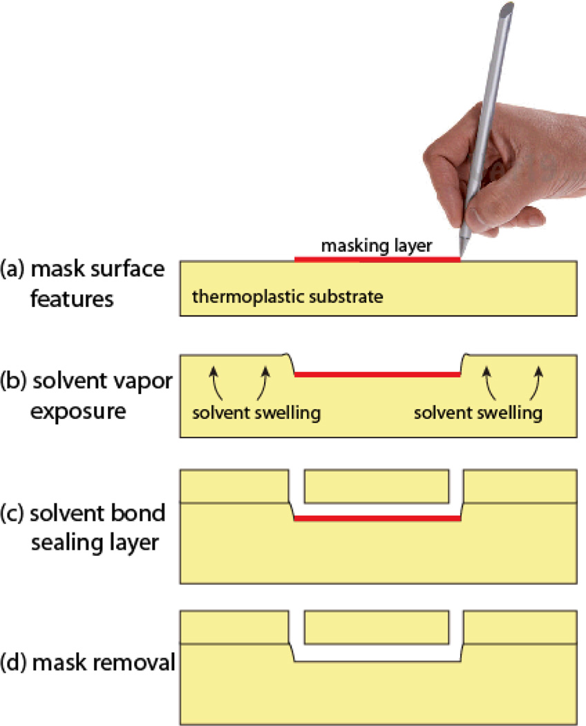
Cyclic olefin copolymers are attractive materials for microfluidic applications due to a range of favorable properties including high optical clarity and low autofluorescence. In comparison with PDMS as an alternative material for rapid prototyping of microchannels, COC offers important advantages such as exceptionally dimensional stability, low water absorption, low gas permeability, and good chemical compatibility with a wide range of alcohols, acids, and bases.30 We recently established that COC materials can exhibit large and permanent surface swelling during gas-phase cyclohexane absorption, with achievable growth heights above 50 µm.21 By masking the COC surface with a solvent-impermeable material, selective patterning of solvent absorption provides a means to form complex raised structures in the COC substrate. In the present work, we explore the application of this orogenic microfabrication process to sealed microchannel fabrication using a commercially available ink deposited from a pen as a masking layer. The basic process is described in Fig. 1. Ink from a pen with a fine-tip felt nib is written onto a COC surface by manual or computer-controlled deposition, followed by exposure to solvent vapor for a specified time required to grow the surface outside of the masked regions by the desired channel height. The solvated surface is then brought into contact with a mating sealing layer comprising a COC chip with pre-drilled fluid ports, resulting in a permanent solvent bond between the layers due to the presence of solvent within the field of the microchannel substrate. Uniform sealing pressure is applied, and the masking ink is removed from the sealed channels by flushing aqueous buffer through the chip. Depending on the desired channel height, the entire process from mask patterning to sealed chip is typically completed within 30–90 min.
Fig. 1.
Overview of the pen microfluidics fabrication process. (a) An ink mask is drawn on a COC chip surface. (b) Vapor-phase solvent exposure results in patterned growth of the COC surface by solvent swelling. (b) Bonding is realized by bringing the patterned surface into contact with a sealing layer, followed by solvent bonding using a desktop laminator. (d) The water-soluble ink masking layer remaining within the sealed microchannel is removed by pumping aqueous buffer through the channel.
Selection of masking ink
Inks are colloidal systems of insoluble pigments or soluble dyes dispersed in an aqueous or organic solvent. For printing on moderately hydrophobic materials such as thermoplastics, inks based on less polar organic solvents are preferred to prevent beading of ink on the polymer surface. Modern inks are complex, with additional components including pH modifiers, dispersants to prevent colloid aggregation, humectants to control drying rate, polymer binders and resins, anti-foaming agents, surfactants, and modifiers to control viscosity.31 Common organic solvents include propylene glycol, propyl alcohol, toluene, and glyco-ethers, with a wide range of pigments or dyes used depending on the desired color, such as eosin (red), copper phthalocyanine or triphenylmethane (blue), titanium dioxide (white), and carbon black (black).32, 31 Unfortunately, the detailed chemistries of commercial inks are generally proprietary, with little information available beyond basic solvent content as determined from manufacturer MSDS data. In the absence of detailed ink composition data, a wide variety of over 20 different commercial inks were experimentally evaluated for use in the pen microfluidics process. During these initial experiments, it was observed that orogenic growth on a COC surface patterned with different inks resulted in different growth heights due to varying levels of resistance to solvent penetration through the masking layer. In some cases large growth heights could be achieved, but only with pinholes forming in the masking layer, resulting in rough channel surfaces. In other cases, smoother channel surfaces were observed, but with maximum growth heights ranging from 20~40 µm regardless of the solvent exposure time, suggesting that cyclohexane was able to uniformly penetrate the ink after sufficient time had elapsed. Of the tested inks, purple ink from a wet-erase marker designed for writing on plastic overhead transparencies was found to be most effective for inhibiting solvent uptake. The solvent system for the selected ink is based on water and propylene glycol.33 Since wet-erase marker solvent content is identical for all of the tested colors, the superior solvent-blocking property of the purple ink is presumably due to the dye used to define this particular ink color. However, other inks may also be used for effective masking within the constraints presented by the observed growth height limitations.
Microchannel width
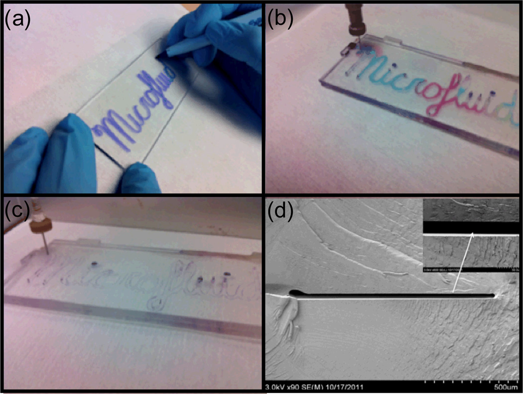
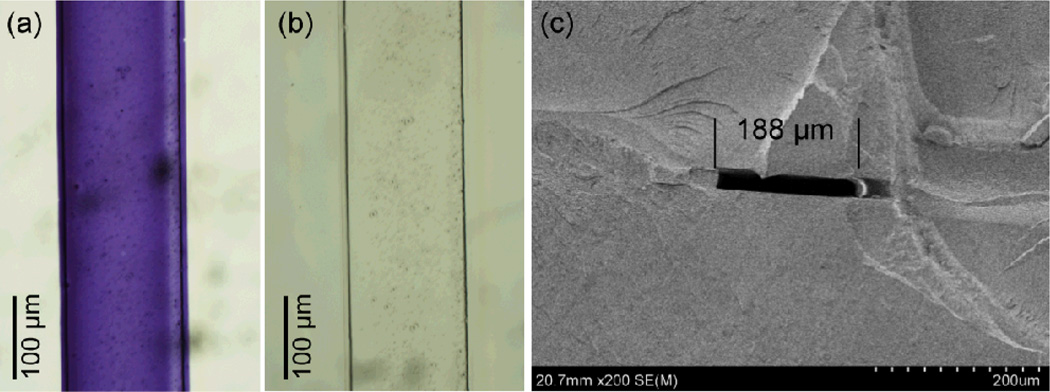
The dimensions of microchannels fabricated in the orogenic process are defined by mask linewidths, with minimum channel widths limited by the pen nib dimensions. Using commercially available wet-erase markers, masking linewidths slightly below 1 mm were reliably formed by manual writing. For example, Figure 2a depicts a chip defined using an ink pattern drawn with ~1 mm lines. After drawing the ink mask, exposing the chip to solvent vapor for 15 min, and sealing the channel, the water-soluble ink was removed by flushing the channels with DI water (Fig. 2b) followed by injection of red food coloring (Fig. 2c) to demonstrate that the channels remain open throughout the process. While low aspect ratio mm-scale channels have been explored for various applications, channels with smaller lateral dimensions are desirable in many microfluidic systems. To achieve smaller mask linewidths, wet-erase marker ink was removed from the native casing and injected into a refillable fiber-tip marker with a reported 200 µm nib diameter. While higher-resolution markers with nib dimensions as small as 30 µm are available, our tests with markers smaller than 200 µm were inconsistent due to irreproducible ink deposition. An example of a straight microchannel fabricated by masking with a marker possessing a nominal nib diameter of 200 µm is shown in Fig. 3, with a measured channel width of 188 µm after sealing.
Fig. 2.
(a) Manual writing with a wet-erase pen onto a COC chip, followed by 15 min orogenic growth and solvent bonding, and sequential sequential injection of (b) water and (c) red food coloring through the resulting microchannel network. (d) SEM image revealing the cross-section of the sealed microchannel.
Fig. 3.
Bright field images of a microchannel formed in a COC chip by orogenic growth with a manually-drawn ink mask (a) immediately after microchannel sealing and (b) following buffer rinsing to remove the water-soluble ink. (c) Cross-sectional SEM image of a typical microchannel, 188 µm wide and 22 µm tall.
Microchannel height
For the channels shown in Fig. 2d and Fig. 3, chip bonding was performed using a hot press after 15 min orogenic growth, resulting in an average channel height of 22 µm in each case. In our prior work exploring the fundamental aspects of orogenic growth using cyclohexane as a solvent for COC, 60 min exposures yielded an average growth height of 51 µm, with nearly linear growth between 5–60 min.21 These growth heights were measured with respect to the masked surface far from the mask boundaries. However, a region of piled-up polymer forms at these boundaries, resulting in localized hillocks of polymer that typically protrude out of the plane of the chip by 40~50% of the overall growth height. Because these raised hillocks act as stress concentration points during chip bonding, application of a high bonding force during channel sealing serves to deform the solvated hillocks, forcing polymer from the raised regions to flow into the open microchannels. In the case of high pressure bonding using a hot press, this polymer reflow results in nearly vertical sidewalls as the hillock volume is displaced into the open channel. This phenomenon can be clearly seen in Fig. 3c.
By extending the solvent exposure time, deeper channels with higher aspect ratios can be achieved. However for channels taller than ~25 µm, swelling of the unmasked regions during extended solvent exposure generates taller hillocks at the edge of the masked area that can uncontrollably fold or collapse into the microchannel when bonding at high pressure, resulting in clogging of the channel by the displaced polymer. To address this problem while making the overall fabrication process compatible with a true desktop manufacturing model, lower bonding pressure was applied using a desktop laminator. The use of the desktop laminator was found to result in significantly less deformation of the raised hillocks, yielding slanted and smooth channel sidewalls without clogging.
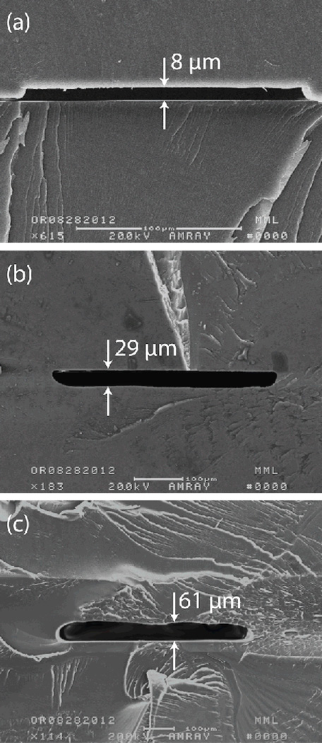
Examples of channels fabricated using different solvent exposure times and bonding methods are presented in Fig. 4. It is significant that final channel heights are higher than previously reported orogenic growth heights alone.21 For example, in the case of a 15 minute solvent exposure time, leading to an orogenic growth height of 17 µm, a final channel height of 22 µm is observed (e.g. Fig. 3). Similarly, a 60 min exposure expected to yield a 51 µm growth height results in a channel height of 61 µm (Fig. 4c). The enhanced channel height is believed to be largely due to the presence of the solvent-swollen polymer hillocks at the mask edge following orogenic growth. A further factor that may contribute to the increased channel height is that solvent absorbed by the orogenically-patterned chip can transfer into the sealing layer during the bonding process, leading to swelling and additional growth of the sealing layer where the chips are in contact. Regardless of the solvent exposure time and bonding method, the final sealing interface is highly planar, with good sealing in the field far from the channels. Bonding strength of the final sealed chips is excellent, with typical burst pressures above 15 MPa as measured using a liquid chromatography pump connected to the chips through high pressure needle ports28.
Fig. 4.
Cross-sectional views of channels fabricated using (a) 8 min, (b) 30 min, and (c) 60 min solvent exposure times, resulting in channel heights of 8 µm, 29 µm, and 61 µm, respectively. In case (a), chip bonding was performed using a hot press, while in cases (b) and (c) a low-pressure lamination process was used for bonding to minimize channel height reduction.
One consideration regarding the orogenic process is whether the solvent-swollen surfaces exhibit different mechanical, chemical, or optical properties compared to the native polymer. Because the swollen polymer possesses a lower density, it is likely that characteristics such as refractive index and bulk modulus are modified during growth. It should be noted that this same issue applies to any thermoplastic surfaces that have been solvent treated during a solvent bonding process, and in fact the orogenically-patterned channels are expected to present surfaces closer to the native polymer since the top and bottom of each channel are protected from solvent exposure during the growth and bonding steps.
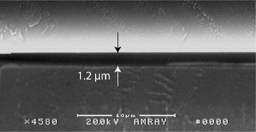
The ink-masking method may also be used to fabricate very low aspect ratio channels through the application of reduced solvent exposure times. Short solvent exposures can produce consistent and controllable growth heights below 200 nm, while maintaining a smooth polymer surface with average surface roughness below 3 nm.21 In principle, this approach can provide a facile alternative to current methods for two-dimensional nanofluidic device fabrication,34–40 since the absence of solvent within the channel regions prevents channel collapse during bonding. However, solvent exposure time also impacts bond strength of the sealed chips, setting a lower limit on achievable channel depth for functional chips. For example, the 1.2 µm deep channel shown in Fig. 5, achieved using a solvent exposure time of 3 min, was found to be near the minimum dimension that could be successfully fabricated without chip delamination during cleavage in preparation for microscopy. Thus while submicron channels are feasible, further efforts are needed to evaluate the limitations of this process.
Fig. 5.
Example of a 1.2 µm tall microchannel with fabricated using a 3 min solvent exposure time. While submicron channel features have been fabricated, solvent exposure times below 3 min result in compromised bond strength for the sealed chips.
Computer-controlled patterning
While manual mask drawing may be suitable for simple microfluidic designs, automated robotic control over mask patterning is necessary more typical applications where pattern accuracy and precision are important considerations. A goal of this work is to demonstrate the pen microfluidic technique as a low-cost desktop manufacturing platform enabling thermoplastic microfluidic fabrication without significant infrastructure investment. To remain aligned to the concept, we evaluated to use of a pen plotter for low-cost automated mask deposition as a replacement for manual drawing. Pen plotters use an automated stage to move a pen cartridge across a drawing surface to create line art. Compared to inkjet printing, an advantage of pen plotting is that a wide range of ink compositions may be used, since the ink is not limited by the viscosity constraints encountered in both piezoelectric and thermal inkjet printing. While consumer-level desktop pen plotters have not been commercially available since the widespread adoption of inkjet and laser printers, an equivalent platform can be assembled by adding a pen holder to an alternative 3-axis robotic positioning system. For example, low-cost vinyl cutter plotters (decal cutters) commonly offer 3-axis position control with high positioning resolution on the order of 10~20 µm.41 Similarly, inexpensive desktop CNC milling machines are available from multiple vendors with suitable positioning accuracy and resolution.
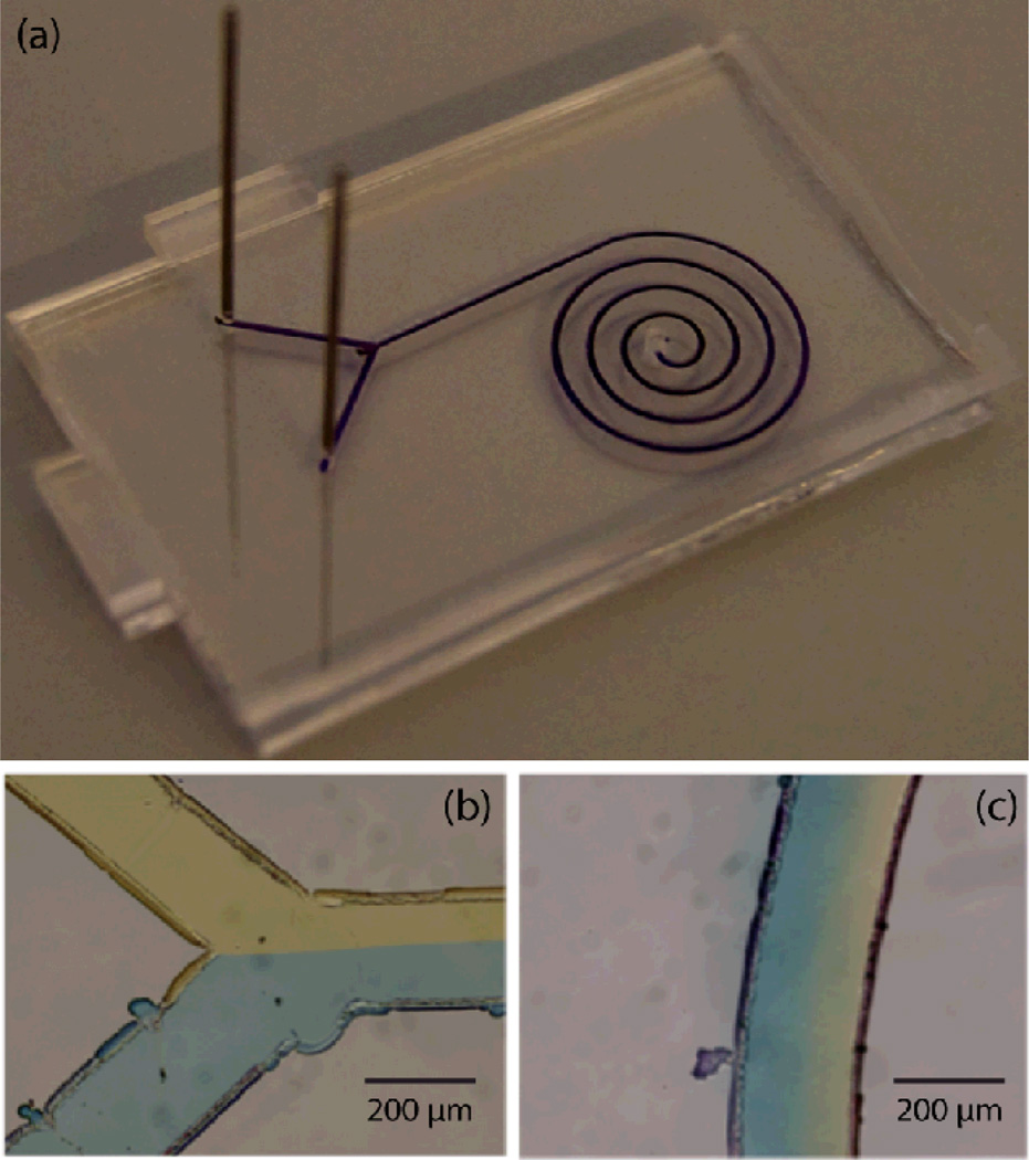
To demonstrate this latter concept, a spiral diffusive mixer design was patterned by mounting a pen on the tool holder of a desktop CNC machine, with the resulting sealed chip shown in Fig. 6. The substrate was exposed to solvent vapor for 15 min, and aligned and bonded to a COC sealing layer with pre-drilled fluid ports. In this device, fluidic access was achieved by inserting stainless steel needle segments into the ports for low dead volume interfacing.28 To demonstrate operation of this device, colored dye solutions were injected through the inlets, with well-defined laminar flow observed at the confluence of the injected streams (Fig. 6b) and formation of a smooth color gradient by diffusion within the downstream arm of the spiral (Fig. 6c). Although portions of the channels exhibited variations in width due to uneven ink deposition during mask patterning, as evident in Fig. 6b, the flow profile within the channels did not appear to be impacted by these defects.
Fig. 6.
Spiral diffusive micromixer fabricated using computer-controlled mask definition. (a) Image of the fully-bonded chip before flushing ink from the enclosed microchannel, and images of dye solutions (b) at the confluence of the injected dye streams and (c) within an arm of the spiral showing formation of a smooth dye gradient due to diffusive mixing.
Conclusion
A desktop manufacturing method for thermoplastic microfluidic devices has been developed, utilizing commercially available inks as a masking layer for solvent-swelling orogenic patterning of the thermoplastic substrates. The photolithography-free fabrication approach combines channel formation and bonding into a single step, where the solvent permeated surface can be permanently bonded to a cap layer to form fully enclosed channels. For manual patterning, the sealed all-thermoplastic chips containing microchannels with lateral dimensions on the order of several hundred microns and heights up to 60 µm may be manufactured with minimal infrastructure consisting of a pen, a solvent dish, and a desktop laminator. Precise computer-generated mask patterns have also been demonstrated by using a modified desktop CNC tool as a pen plotter. The masking ink may also be patterned by inkjet deposition using a commercial piezoelectric print head, following appropriate modification of the ink viscosity. The simplicity of this approach allows a designer to directly define channel features on a thermoplastic substrate, with total cycle times between 30–90 minutes from initial design concept to final device. This process offers a unique and exceptionally rapid approach to prototyping patterned and sealed microfluidic devices from homogeneous thermoplastic substrates.
Acknowledgements
This research was supported in part by NIH grants R21EB011750 and R21EB009485, and by the DARPA N/MEMS S&T Fundamentals Program under grant no. N66001-1-4003 issued by the Space and Naval Warfare Systems Center Pacific (SPAWAR) to the Micro/nano Fluidics Fundamentals Focus (MF3) Center. Electron microscopy was performed with support from the University of Maryland Nanoscale Imaging, Spectroscopy, and Properties Laboratory (NISPLab).
References
- 1.Xia Y, Whitesides GM. Annual Review of Materials Science. 1998;28:153–184. [Google Scholar]
- 2.Lee JN, Park C, Whitesides GM. Analytical Chemistry. 2003;75:6544–6554. doi: 10.1021/ac0346712. [DOI] [PubMed] [Google Scholar]
- 3.Lucio do Lago C, Torres da Silva HD, Neves CA, Alves Brito-Neto JG, Fracassi da Silva JA. Analytical chemistry. 2003;75:3853–3858. doi: 10.1021/ac034437b. [DOI] [PubMed] [Google Scholar]
- 4.Liu A, He F, Wang K, Zhou T, Lu Y, Xia X. Lab Chip. 2005;5:974. doi: 10.1039/b502764k. [DOI] [PubMed] [Google Scholar]
- 5.Coltro WKT, De Jesus DP, Da Silva JAF, Do Lago CL, Carrilho E. Electrophoresis. 2010;31:2487–2498. doi: 10.1002/elps.201000063. [DOI] [PubMed] [Google Scholar]
- 6.Lausted CG, Warren CB, Hood LE, Lasky SR. Methods in Enzymology. 2006;410:168–189. doi: 10.1016/S0076-6879(06)10008-7. [DOI] [PubMed] [Google Scholar]
- 7.Do J, Zhang JY, Klapperich CM. Robotics and Computer-Integrated Manufacturing. 2011;27:245–248. [Google Scholar]
- 8.Nath P, Fung D, Kunde YA, Zeytun A, Branch B, Goddard G. Lab on a Chip. 2010;10:2286–2291. doi: 10.1039/c002457k. [DOI] [PubMed] [Google Scholar]
- 9.Yuen PK, Goral VN. Lab on a Chip. 2010;10:384–387. doi: 10.1039/b918089c. [DOI] [PubMed] [Google Scholar]
- 10.Martynova L, Locascio LE, Gaitan M, Kramer GW, Christensen RG, MacCrehan WA. Analytical Chemistry. 1997;69:4783–4789. doi: 10.1021/ac970558y. [DOI] [PubMed] [Google Scholar]
- 11.Xu JD, Locascio L, Gaitan M, Lee CS. Anal. Chem. 2000;72:1930–1933. doi: 10.1021/ac991216q. [DOI] [PubMed] [Google Scholar]
- 12.Hansen TS, Selmeczi D, Larsen NB. Journal of Micromechanics and Microengineering. 2010;20:015020. [Google Scholar]
- 13.Truckenmüller R, Giselbrecht S, Rivron N, Gottwald E, Saile V, Van Den Berg A, Wessling M, Van Blitterswijk C. Advanced materials Deerfield Beach Fla. 2011;23:1311–1329. doi: 10.1002/adma.201003538. [DOI] [PubMed] [Google Scholar]
- 14.Liedert R, Amundsen LK, Hokkanen A, Mäki M, Aittakorpi A, Pakanen M, Scherer JR, Mathies RA, Kurkinen M, Uusitalo S, Hakalahti L, Nevanen TK, Siitari H, Söderlund H. Lab on a Chip. 2011;12:333–339. doi: 10.1039/c1lc20782b. [DOI] [PubMed] [Google Scholar]
- 15.Velten T, Schuck H, Richter M, Klink G, Bock K, Malek CK, Roth S, Schoo H, Bolt PJ. J. Eng. Manufact. 2008;222:107–116. [Google Scholar]
- 16.Rötting O, Röpke W, Becker H, Gärtner C. Microsystem Technologies. 2002;8:32–36. [Google Scholar]
- 17.Becker H, Locascio LE. Talanta. 2002;56:267–287. doi: 10.1016/s0039-9140(01)00594-x. [DOI] [PubMed] [Google Scholar]
- 18.Becker H, Gärtner C. Electrophoresis. 2000;21:12–26. doi: 10.1002/(SICI)1522-2683(20000101)21:1<12::AID-ELPS12>3.0.CO;2-7. [DOI] [PubMed] [Google Scholar]
- 19.Becker H, Gärtner C. Analytical and Bioanalytical Chemistry. 2008;390:89–111. doi: 10.1007/s00216-007-1692-2. [DOI] [PubMed] [Google Scholar]
- 20.Do J, Zhang JY, Klapperich CM. Robotics and Computer-Integrated Manufacturing. 2011;27:245–248. [Google Scholar]
- 21.Rahmanian O, Chen C-F, DeVoe DL. Langmuir. 2012;28:12923–12929. doi: 10.1021/la302704t. [DOI] [PMC free article] [PubMed] [Google Scholar]
- 22.Kim E, Xia Y, Zhao X-M, Whitesides GM. Advanced Materials. 1997;9:651–654. [Google Scholar]
- 23.Suh K-Y, Park MC, Kim P. Advanced Functional Materials. 2009;19:2699–2712. doi: 10.1002/adfm.200990041. [DOI] [PMC free article] [PubMed] [Google Scholar]
- 24.Suh KY, Lee HH. Advanced Functional Materials. 2002;12:405–413. [Google Scholar]
- 25.Wallow TI, Morales AM, Simmons BA, Hunter MC, Krafcik KL, Domeier LA, Sickafoose SM, Patel KD, Gardea A. Lab on a Chip. 2007;7:1825–1831. doi: 10.1039/b710175a. [DOI] [PubMed] [Google Scholar]
- 26.Ro KW, Liu H, Knapp DR. Journal of Chromatography A. 2006;1111:40–47. doi: 10.1016/j.chroma.2006.01.105. [DOI] [PubMed] [Google Scholar]
- 27.Tsao C-W, Kumar P, Liu K, DeVoe DL. Anal. Chem. 2008;80:2973–2981. doi: 10.1021/ac7026029. [DOI] [PubMed] [Google Scholar]
- 28.Chen CF, Liu J, Hromada LP, Tsao CW, Chang CC, DeVoe DL. Lab Chip. 2009;9:50–55. doi: 10.1039/b812812j. [DOI] [PubMed] [Google Scholar]
- 29.Chen C-F, Liu J, Chang C-C, DeVoe DL. Lab Chip. 2009;9:3511–3516. doi: 10.1039/b912014a. [DOI] [PubMed] [Google Scholar]
- 30.Shin JY, Park JY, Liu C, He J, Kim SC. Pure and Applied Chemistry. 2005;77:801–814. [Google Scholar]
- 31.Kunjappu JT. Essays in Ink chemistry. New York: Nova Science Publishers; 2001. [Google Scholar]
- 32.Kenyon RW. In: Chemical technology in printing and imaging systems. Gregory P, editor. London: Blackie; 1996. [Google Scholar]
- 33.Material Safety Data Sheet for Vis-A-Vis Waterbased Transparency Marker. 2001 [Google Scholar]
- 34.Xia D, Yan J, Hou S. Small. 2012 doi: 10.1002/smll.201200240. DOI 10.1002/smll.201200240. [DOI] [PubMed] [Google Scholar]
- 35.Xu BY, Xu JJ, Xia XH, Chen HY. Lab Chip. 2010;10:2894–2901. doi: 10.1039/c005245k. [DOI] [PubMed] [Google Scholar]
- 36.Hamblin MN, Xuan J, Maynes D, Tolley HD, Belnap DM, Woolley AT, Lee ML, Hawkins AR. Lab Chip. 2010;10:173–178. doi: 10.1039/b916746c. [DOI] [PubMed] [Google Scholar]
- 37.Chantiwas R, Hupert ML, Pullagurla SR, Balamurugan S, Tamarit-López J, Park S, Datta P, Goettert J, Cho Y-K, a Soper S. Lab on a chip. 2010;10:3255–3264. doi: 10.1039/c0lc00096e. [DOI] [PubMed] [Google Scholar]
- 38.Fu J, Yoo J, Han J. Physical Review Letters. 2006;97:18103. doi: 10.1103/PhysRevLett.97.018103. [DOI] [PMC free article] [PubMed] [Google Scholar]
- 39.O’Brien MJ, Bisong P, Ista LK, Rabinovich EM, Garcia AL, Sibbett SS, Lopez GP, Brueck SRJ. J. Vac. Sci. Technol. B. 2003;21:2941–2945. [Google Scholar]
- 40.Huang LRLR, Tegenfeldt JOJO, Kraeft JJJJ, Sturm JCJC, Austin RHRH, Cox ECEC. A DNA prism for high-speed continuous fractionation of large DNA molecules. 2002;vol. 20 doi: 10.1038/nbt733. [DOI] [PubMed] [Google Scholar]
- 41.Bartholomeusz DA, Boutte RW, Andrade JD. J. MEMS. 2005;14:1364–1374. [Google Scholar]


