Abstract
High aspect ratio Ni nanowires (NWs) and nanotubes (NTs) were electrodeposited inside ordered arrays of self-assembled pores (approximately 50 nm in diameter and approximately 50 μm in length) in anodic alumina templates by a potentiostatic method. The current transients monitored during each process allowed us to distinguish between NW and NT formation. The depositions were long enough for the deposited metal to reach the top of the template and form a continuous Ni film. The overfilling process was found to occur in two steps when depositing NWs and in a single step in the case of NTs. A comparative study of the morphological, structural, and magnetic properties of the Ni NWs and NTs was performed using scanning electron microscopy, X-ray diffraction, and vibrating sample magnetometry, respectively.
Keywords: Electrodeposition, Crystallographic texture, Ordered arrays, Nickel, Nanoporous alumina templates
Background
One-dimensional metallic nanostructured materials have attracted extensive attention in recent years because of their technological importance in nanometer-scale devices and information storage systems [1-6]. By combining deposition techniques with nanoporous templates, one can easily tune the growth of these nanostructures and form concentric and multisegmented nanotubes (NTs) and nanowires (NWs) [7-10].
A large number of works have focused on magnetic NWs embedded in ordered arrays of self-assembled pores in alumina membranes [11-17]. However, only a few works have been reported on ordered arrays of magnetic NTs [18-22]. These novel nanostructures have recently attracted much interest due to their inner functionalizable surfaces that can be used for drug delivery [23-25] and also owing to their interesting magnetic behavior [20-22]. In particular, Ni NTs have been prepared in nanoporous membranes by triblock copolymer-assisted hard-template method [26], electroplating [27], a sequential electrochemical synthetic method inside conducting polypyrrole NTs [8], and using chemically modified templates [28].
In recent reports, the magnetic behavior of arrays of magnetic NTs was investigated [8,20-22,26-28]. Nevertheless, there are a number of different parameters that seem to lead to diverse results. For example, Wang et al.[22] found higher remanence values for Ni NT arrays with different diameters (25 to 220 nm) when applying the field parallel to the nanotube's axis, evidencing the important role played by shape anisotropy in the magnetic hysteresis loops. However, other works showed that the easy axis of Ni NT arrays with diameters of approximately 200 nm is perpendicular to the tube axis [21,26,28]. Such differences are related to the distinct preparation methods, geometrical characteristics, ordering degree of hexagonal symmetry, or the final crystalline structure of the magnetic elements. Polycrystalline Ni NWs and NTs, with 45-nm diameters, fabricated using a direct-current electrodeposition method also showed similar magnetic hysteresis loops for both NW and NT arrays [27]. In the present work, we used a potentiostatic electrodeposition method to grow Ni NWs and NTs strongly textured along the [110] direction, showing different coercivity values along the parallel direction. One should also note that few reports can be found on the preparation of small-diameter (<60 nm) Ni NT arrays [22,27]. Reducing the diameter of these tube-like nanostructures, one expects to increase their coercivity and remanence values along the parallel direction.
The objective of the present work is to address a comparative analysis of the careful preparation of Ni NW and NT arrays with well-controlled ordering and their structural and magnetic response. These nanostructures were prepared by potentiostatic electrodeposition of Ni into suitably modified nanoporous alumina templates (NpATs) opened from both top and bottom sides [17]. Long-range ordering of hexagonal symmetry of the alumina membranes with 105-nm interpore distance and 50-nm pore diameter was achieved [29,30]. The final NW/NT diameter was approximately 50 nm, while the NTs' wall thickness was approximately 5 nm, and their length corresponded to the membrane thickness (50 μm). The time of deposition was controlled by the overfilling process in which a Ni continuous film was formed on top of the membrane. In this work, we found this process to be considerably different when depositing NWs or NTs inside the pores. A thorough comparative study of the current transients monitored during the electrodeposition process showed a clear distinction between NW and NT formation. The presence of Ni NWs and NTs inside the nanopores was also confirmed by scanning electron microscopy (SEM).
Methods
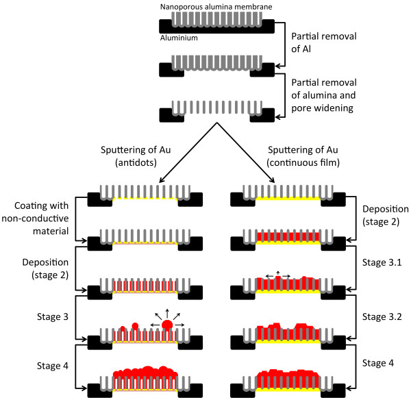
Ni was electrodeposited inside self-assembled pores of anodic alumina membranes (approximately 50 nm in pore diameter, approximately 105 nm in interpore distance, and approximately 50 μm thick) using a three-electrode cell in a potentiostatic mode. The NpATs were prepared by a two-step anodization process of high-purity (99.999%) aluminum disks in 0.3 M oxalic acid at 40 V and 5°C [30]. First and second anodizations were performed during 24 and 20 h, respectively. The Al substrate was then removed on the backside of the membrane by chemical etching in an aqueous solution of 0.2 M CuCl2 and 4.1 M HCl, and the pores widened and opened at the bottom using 0.5 M phosphoric acid at room temperature (Figure 1). Further details on the membrane preparation can be found elsewhere [17].
Figure 1.
Stages in the fabrication of NW and NT arrays in NpATs by potentiostatic deposition.
For the deposition of NWs, a 100-nm-thick Au film was sputtered at the opened pores' bottom of the NpAT to serve as the working electrode. In the case of NT formation, a thinner (approximately 40 nm thick) Au layer was sputtered so as not to completely close the bottom of the pores [31]. To avoid leaking of the electrolyte at the opened membrane bottom, a non-conductive varnish was coated on top of the 40-nm-thick Au contact (Figure 1). A Pt mesh was used as the counter electrode and Ag/AgCl (in 4 M KCl) as the reference electrode (0.197 V vs. standard hydrogen electrode). The depositions were performed in a Watts bath (1.14 M NiSO4·6H2O, 0.19 M NiCl2·6H2O, and 0.73 M H3BO3) at −1.5 V vs. Ag/AgCl, using a Solartron 1480 MultiStat (Solartron Analytical, Farnborough, Hampshire, UK). During the electrodeposition, the electrolyte was magnetically stirred at 250 rpm and kept at a constant temperature of 35°C within a pH range between 3.5 and 4 [32].
To explore the differences between NW and NT formation, the depositions were performed until a continuous Ni film was formed on top of the NpAT. Different stages were then found in the overfilling process, and to better understand them, several experiments were made, stopping the deposition at each stage (Figure 1).
Prior to NW and NT characterization, the Ni film formed on top of the NpAT was removed by mechanical polishing using alumina powder (particle size of 10 μm). The mechanical polishing was only performed on the upper surface of the nanoporous alumina template, in order to remove the Ni caps that overfilled and are present at the membranes' top, without causing any damage to the electrodeposited nanostructures. The remaining Ni caps on top of the NpATs were then completely etched by ion milling (5 to 10 μm). The milling process was carried out using an ion beam sputter deposition system by the Commonwealth Scientific Corporation [15]. Morphological characterization was performed using SEM (FEI Nova NanoSEM 230 and FEI Quanta 400FEG, FEI Co., Eindhoven, The Netherlands). Structural analysis was performed by X-ray diffraction (XRD; PANalytical X'Pert Pro, PANalytical B.V., Almelo, The Netherlands) using Cu Kα1 radiation (λ = 0.15406 nm) and the Bragg-Brentano θ/2θ geometry [33]. The deposited NWs and NTs were magnetically characterized using a vibrating sample magnetometer (VSM; LOT-Oriel EV7, LOT-Oriel, Leatherhead, Surrey, UK).
Results and discussion
Structural and morphological properties
Smooth and well-defined high aspect ratio (length/diameter approximately 1,000) Ni NWs and NTs were fabricated. For cross-sectional SEM images, the filled NpATs were broken and observed in the vertical fractured region (Figure 2a,d). Prior to top and bottom SEM imaging, ion milling was performed to remove the Au contact at the bottom (1 μm) and the Ni caps on top (5 to 10 μm) and to smoothen the NpAT surface (Figure 2b,c,e,f). Pore filling percentage is approximately 100% for Ni NWs grown in a NpAT by potentiostatic deposition (Figure 2b,c). The obtained NWs were approximately 50 nm in diameter and approximately 50 μm in length, corresponding to the pore diameter and template thickness, respectively. On the other hand, we observe that the fabrication of Ni NTs leads to only approximately 40% pore filling (Figure 2e), which we attribute to the fact that the nonmetallic coating enters some of the pores and covers the inner Au contact, avoiding subsequent Ni deposition. The optimization of the coating process and material deposition is underway, aiming for 100% NT formation. However, notice that as reported before [15], the obtained percentage of pore filling does not influence the magnetic properties. Additionally, Figure 2d,e,f clearly shows that the NT outer diameter correspond to the pore diameter (approximately 50 nm), and their wall is smooth and uniform, evidencing a constant thickness value (tw approximately 5 nm) throughout the whole nanopore. Figure 2f also shows that some NTs do not reach the upper end of the nanopores. This is because the Ni film overgrown on top will cover some of the pores before they can be completely filled with NTs.
Figure 2.
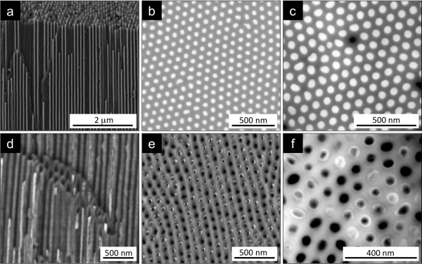
SEM images of Ni NWs (a, b, c) and NTs (d, e, f) in NpATs. Cross-sectional (a, d), bottom (b, e, after 1-μm milling), and top (c, f, after 5-μm milling) views.
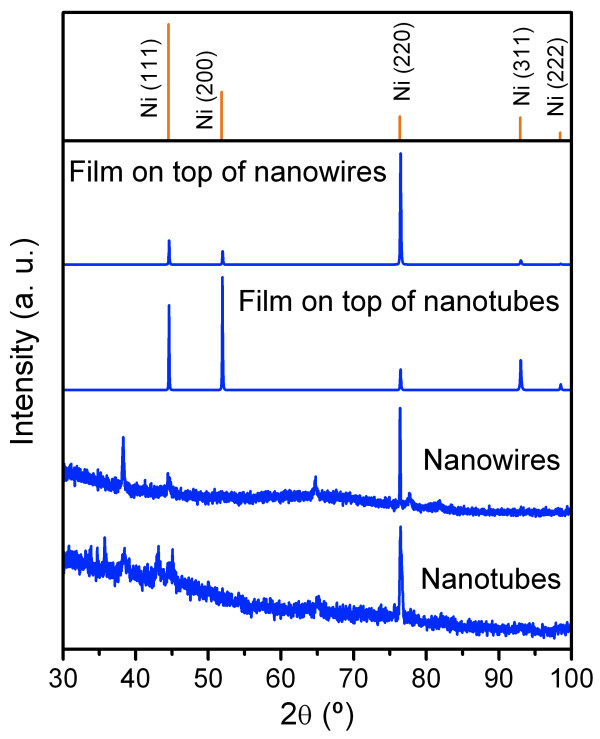
XRD measurements illustrate a face-centered cubic (fcc) Ni pattern for the NWs and NTs in NpATs and for the continuous film overgrown on top (Figure 3). The Ni NWs and NTs were found strongly textured along the [110] direction (Figure 3), seemingly due to the nanopores' geometrical confinement [17]. However, the continuous film formed on top exhibits four different peaks that correspond to the (111), (200), (220), and (311) planes of fcc Ni (Figure 3). The Ni crystallite size of the deposited nanostructures was estimated using the Sherrer equation [34], giving 90 ± 10 nm and 40 ± 10 nm for the Ni NWs and NTs, respectively. This is consistent with the fact that both nanostructures have the same outer diameter of approximately 50 nm (corresponding to the nanopores' diameter), but the NTs present a core cylindrical hole with an estimated diameter of approximately 40 nm. Therefore, the NTs' crystallite size is much smaller as it corresponds to a thin film of approximately 5 nm wrapped in a cylindrical shape.
Figure 3.
XRD patterns of Ni NWs, NTs, and films overgrown on top after electrodeposition in NpAT.
The average crystallite sizes of the continuous Ni film overgrown on top of the NpATs were estimated to be of 70 ± 10 nm for the Ni film formed after overgrowth of NWs and 75 ± 10 nm for the Ni film grown on top of NTs. The grain size of an electrodeposited film is known to strongly depend on the electrodeposition conditions (applied potential, electrolyte composition, temperature, pH, agitation, etc.) and substrate used [35-38]. For both Ni films overgrown on top of NWs or NTs, the deposition conditions were kept the same. However, the substrates on which the films start to grow have different geometries (Figure 4). At the moment when the NWs start overfilling the membrane, their sectional area, which corresponds to approximately 20% of the total membrane's area, has a preferential crystallographic texture along the [110] direction. According to previous works [39,40], a deposited material will favorably grow epitaxially on oriented grains in the substrate. Therefore, the Ni film overgrown on top of the NWs will continue to exhibit a textured growth orientation along the [110] direction (Figure 3). Nonetheless, since a lateral growth will also start to occur, different grain orientations (along the [111] and [100] directions) can also be found on the Ni film formed.
Figure 4.

Schematic representations of the preferential growth directions of the deposited material. Growth directions on top of a nanotube (left) and nanowire (right).
As for the NTs, their deposition area is approximately 40% of the NWs' area, and their geometry will favor the metal deposition to occur without a preferred orientation (Figure 4). One therefore finds different Ni grain orientations on the film grown on top of the NTs, exhibiting a preferential crystallographic texture along the [100] direction.
Current transients during deposition
The depositions of Ni inside the nanopores were performed until the metal reached the top of the membrane and formed a continuous Ni film. During the complete process of deposition, from the nucleation at the Au contact at the bottom of the pores until the formation of a continuous metallic film on top of the membrane, several stages of metal deposition can be identified. Figure 5a,b illustrates the current transient during Ni NW and NT deposition inside the nanopores, respectively, and the overfilling process that leads to the continuous film on top. The nucleation at the Au contact (stage 1) is similar for both nanostructures and has already been described in the literature [41]. During metal growth inside the nanopores (stage 2), the current is approximately constant for the NT formation, corresponding to a constant wall thickness formation throughout the whole tube. However, during NW growth, it slightly increases (by around 4% of its initial value), illustrating the small enlargement of the pore diameter due to the pore widening process when opening the pores' bottom. In fact, one should note that a small enlargement of approximately 2% in the pore diameter from the lower to the upper part of the membrane results in an approximately 4% raise of the effective deposition area, due to an increase of the membrane's porosity, in good agreement with the current increase seen during deposition.
Figure 5.
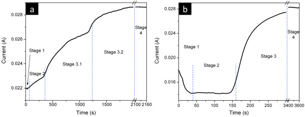
Current transients during Ni NW (a) and NT (b) deposition in NpATs.
The main difference found between NW and NT formation occurs when Ni reaches the end of the pores, starting to deposit on top of the membrane. The current transients monitored during this overfilling process allowed us to characterize whether NTs or NWs had grown inside the pores. When NWs are being deposited, the metal overfilling occurs in a two-step process (stages 3.1 and 3.2 in Figure 5a). During the deposition of NWs inside the pores, the electrode area corresponds to the membranes' porosity (approximately 20%). As the first NWs reach the upper end of the pores, they start to form polygonal-shaped caps of Ni on top of the NpAT (Figure 6). These will enlarge the electrode area and therefore increase the deposition current (stage 3.1). When the surface area associated with the deposition of Ni on top of the membrane becomes higher than the area of the remaining opened pores, where NWs are still being formed, a second sudden increase in the deposition current occurs (stage 3.2). At this point, the metallic layer being deposited on top of the NpAT becomes the main cathode surface. Therefore, the current will preferentially flow into the metal film being formed on top, increasing the rate of the metallic layer deposition and decreasing the NW growth rate inside the pores.
Figure 6.

Cross-sectional (a) and top (b) SEM images of polygonal caps. These are formed at the NpAT surface when Ni NWs start to overfill, forming a continuous Ni film on top (c).
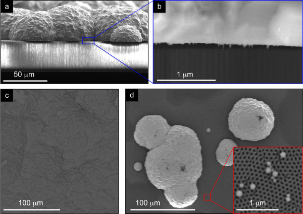
On the other hand, once NTs are present inside the pores, their overfill process occurs in a one-step manner (stage 3 in Figure 5b). During the NT growth inside the pores, the cathode deposition surface is less than 5% of the total NpAT area exposed to the electrolyte. Therefore, as the first NTs emerge and start overfilling, the effective deposition area is drastically enlarged, as confirmed by the sharp increase of the current (stage 3 in Figure 5b). Additionally, the caps formed at the NpAT surface display a spherical shape without well-defined facets (Figure 7). This phenomenon will largely influence the increase in current occurring in only one stage. One should note that as soon as a few spheres are formed on top, the cathode surface area increases to a higher value than the effective area of NT deposition inside the nanopores. Stage 3 of NT deposition should therefore be equivalent to stage 3.2 of NW deposition. Since for the NW growth this only occurs after a small amount of Ni film was already formed on top (during stage 3.1), the overfilling process will exhibit two steps during stage 3 (Figure 1).
Figure 7.
Cross-sectional (a, b) and top (c, d) SEM images of spherical polycrystalline caps. These are formed at the NpAT surface when Ni NTs start to overfill (d), creating a continuous Ni film on top (c).
When considering the current data from Figure 5 together with the XRD data of Figure 3, one can see that the high current increase, observed when the NTs start overfilling, helps promote the growth orientations along the [211] and [100] directions while lowering [110] texture. However, when the NWs overfill, the current increase is smoother than in the case of the NTs (Figure 5), therefore promoting with less evidence the Ni crystal growth along the [211] and [100] directions (Figure 3).
After complete covering of the nanopores, a continuous Ni film grows at the NpAT surface. This corresponds to stage 4 of deposition (Figure 1), exhibiting a constant current transient, associated with the constant cathode surface area (Figure 5). The deposited films presented different surface morphologies depending on whether NWs or NTs were overfilled. For NWs, it shows smooth facets corresponding to the agglomeration of polygonal caps, typical of crystals with mixed [100] and [110] textures (Figure 6c), while for NTs, it results from the superposition of spherical caps, typical of almost randomly oriented crystals with [100], [110], and [211] textures (Figure 7c). However, in both cases, if a continuous Ni film is formed on top, it then easily detaches from the membrane (Figure 8a). In this way, one can fabricate NpATs with their pores completely filled with NWs or NTs, removing in an easy way all the undesired caps formed on top. The careful observation of the bottom side of the detached Ni film allowed us to visualize the ordered hexagonal pattern printed by the NpAT, and some NWs (Figure 8b) and NTs (Figure 8c) that were broken upon lifting the Ni film. These are, however, very small in length (approximately 100 to 200 nm), corresponding to approximately 0.2% to 0.4% of their total length, and thus will not influence the structural and magnetic properties of the array [15]. The observation of small fractions of NTs at the bottom side of the detached Ni film provides additional evidence that the NTs reach the top of the membrane, maintaining their tubular structure.
Figure 8.

SEM images of the Ni film formed on top of the NpAT. Cross-sectional view of respective lift off after NW deposition (a) and Ni film's bottom view after NW (b) and NT (c) deposition.
Magnetic properties
The magnetic behavior of the fabricated samples was studied using a VSM in two different magnetic field configurations: parallel (//, ϕ = 0°) and perpendicular (⟂, ϕ = 90°) modes, according to the angle ϕ between the applied field and the NW/NT long axis. Magnetic hysteresis loops of Ni NWs and NTs grown in ordered NpATs are presented in Figure 9a,b, respectively. From a straightforward comparison between parallel- and perpendicular-direction hysteresis loops, we can deduce that the easy magnetization direction is parallel to the NW/NT long axis, and the perpendicular direction is a magnetization hard direction. The easy direction is ascribed to the shape anisotropy of the NWs/NTs [16,17,42].
Figure 9.
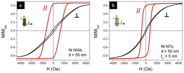
Magnetic hysteresis loops of Ni NW (a) and NT (b) arrays in NpATs. The hysteresis loops were measured in the parallel (//, red) and perpendicular (⟂, black) directions.
The longitudinal anisotropy of the NW/NT arrays is confirmed by the large remanence in the //-direction loop that nearly reaches the saturation magnetization (MSat) value. The coercive field (HC) is approximately 1,000 Oe for the NW and approximately 600 Oe for the NT arrays, in good agreement with the values reported in previous works [16,22,27]. Seemingly, the longitudinal remagnetization involves the presence of a domain wall-like process. Perpendicular hysteresis loops show reduced coercivity (approximately 100 Oe) and the presence of a magnetization rotation reversal mode. Values of the longitudinal anisotropy field can be derived (from extrapolation of initial susceptibility) to be approximately 3,500 and 2,500 Oe for NWs and NTs, respectively, in agreement with the reduced longitudinal coercivity observed for NTs. One should note that the preparation of NTs with small diameters (<60 nm) is a laborious process and very difficult to achieve [43], so most of the reports on magnetic measurements in NT arrays correspond to NTs with outer diameters of approximately 200 nm. For these nanostructures, one finds very small coercive fields (<100 Oe) and remanence (approximately 0.05) along the //-direction [8,20,21,26,28]. However, Wang et al.[22,27] found that coercivity and remanence along the //-direction increase with the decrease of the outer diameter, obtaining an HC//of approximately 610 Oe for outer diameters of approximately 45 nm.
Conclusions
In this work, we fabricated Ni NW and NT arrays in NpATs by a potentiostatic electrodeposition process using a three-electrode cell. The monitorization of the current transients during deposition allowed us to distinguish between NW and NT formation and identify the four main stages of deposition in nanoporous membranes. The overfilling of the deposited metal was found to occur in a two-step process for the NWs and only in one step for the NTs. Morphological and structural characterization of the Ni NWs, NTs, and film overgrown on top of the membrane was performed by SEM and XRD. Both NWs and NTs exhibit a preferential crystallographic growth textured along the [110] direction. The films overgrown on top illustrated the presence of Ni grains oriented along the [111], [100], and [110] directions. The Ni NWs overgrow with a preferential orientation along the [110] direction, showing polygonal-shaped caps at the surface of the membrane. On the other hand, the Ni film on top of the NTs exhibits a preferential growth along the [100] direction and an agglomeration of spherical polycrystalline caps. Magnetic hysteresis loops illustrate a magnetization easy axis parallel to the long axis for both NW and NT arrays, exhibiting stronger anisotropy and higher coercivity values for the NW arrays.
Competing interests
The authors declare that they have no competing interests.
Authors’ contributions
MPP prepared the samples, characterized them, and wrote the main part of the manuscript. CTS, JV, MV, and JPA conceived the study, participated in the interpretation of the results, and contributed in drafting the manuscript. All authors read and approved the final manuscript.
Contributor Information
Mariana P Proenca, Email: mpproenca@fc.up.pt.
Célia T Sousa, Email: celiasousa@fc.up.pt.
João Ventura, Email: joventur@fc.up.pt.
Manuel Vazquez, Email: mvazquez@icmm.csic.es.
João P Araujo, Email: jearaujo@fc.up.pt.
Acknowledgments
M. P. Proença and C. T. Sousa are thankful to FCT for the doctoral and postdoctoral grants SFRH/BD/43440/2008 and SFRH/BPD/82010/2011, respectively. J. Ventura acknowledges the financial support through FSE/POPH. M Vázquez thanks the Spanish Ministry of Economia y Competitividad, MEC, under project MAT2010-20798-C05-01. J. P. Araújo also thanks the Fundação Gulbenkian for its financial support within the ‘Programa Gulbenkian de Estímulo à Investigação Científica’. The authors acknowledge the funding from FCT through the Associated Laboratory - IN and project PTDC/FIS/105416/2008.
References
- Byrne F, Prina-Mello A, Whelan A, Mohamed BM, Davies A, Gun’ko YK, Coey JMD, Volkov Y. High content analysis of the biocompatibility of nickel nanowires. J Magn Magn Mater. 2009;7:1341–1345. doi: 10.1016/j.jmmm.2009.02.035. [DOI] [Google Scholar]
- Stashkevich AA, Roussigné Y, Djemia P, Chérif SM, Evans PR, Murphy AP, Hendren WR, Atkinson R, Pollard RJ, Zayats AV, Chaboussant G, Ott F. Spin-wave modes in Ni nanorod arrays studied by Brillouin light scattering. Phys Rev B. 2009;7:144406. [Google Scholar]
- Boone CT, Katine JA, Childress JR, Tiberkevich V, Slavin A, Zhu J, Cheng X, Krivorotov IN. Resonant nonlinear damping of quantized spinwaves in ferromagnetic nanowires: a spin torque ferromagnetic resonance study. Phys Rev Lett. 2009;7:167601. doi: 10.1103/PhysRevLett.103.167601. [DOI] [PubMed] [Google Scholar]
- Chen S-F, Wei HH, Liu C-P, Hsu CY, Huang JCA. Microstructural effects on the magnetic and magneto-transport properties of electrodeposited Ni nanowire arrays. Nanotechnology. 2010;7:425602. doi: 10.1088/0957-4484/21/42/425602. [DOI] [PubMed] [Google Scholar]
- Banerjee AN, Qian S, Joo SW. Large field enhancement at electrochemically grown quasi-1D Ni nanostructures with low-threshold cold-field electron emission. Nanotechnology. 2011;7:035702. doi: 10.1088/0957-4484/22/3/035702. [DOI] [PubMed] [Google Scholar]
- Kou X, Fan X, Dumas RK, Lu Q, Zhang Y, Zhu H, Zhang X, Liu K, Xiao JQ. Memory effect in magnetic nanowire arrays. Adv Mater. 2011;7:1393–1397. doi: 10.1002/adma.201003749. [DOI] [PubMed] [Google Scholar]
- Chen HM, Liu R-S. Architecture of metallic nanostructures: synthesis strategy and specific applications. J Phys Chem C. 2011;7:3513–3527. doi: 10.1021/jp108403r. [DOI] [Google Scholar]
- Park DH, Lee YB, Cho MY, Kim BH, Lee SH, Hong YK, Joo J, Cheong HC, Lee SR. Fabrication and magnetic characteristics of hybrid double walled nanotube of ferromagnetic nickel encapsulated conducting polypyrrole. Appl Phys Lett. 2007;7:093122. doi: 10.1063/1.2710748. [DOI] [Google Scholar]
- Lee W, Scholz R, Nielsch K, Gösele U. A template-based electrochemical method for the synthesis of multisegmented metallic nanotubes. Angew Chem Int Ed. 2005;7:6050–6054. doi: 10.1002/anie.200501341. [DOI] [PubMed] [Google Scholar]
- Karim S, Maaz K. Magnetic behavior of arrays of nickel nanowires: effect of microstructure and aspect ratio. Mater Chem Phys. 2011;7:1103–1108. doi: 10.1016/j.matchemphys.2011.08.039. [DOI] [Google Scholar]
- Leitao DC, Sousa CT, Ventura J, Amaral JS, Carpinteiro F, Pirota KR, Vazquez M, Sousa JB, Araujo JP. Characterization of electrodeposited Ni and Ni80Fe20 nanowires. J Non-Cryst Solids. 2008;7:5241–5243. doi: 10.1016/j.jnoncrysol.2008.05.088. [DOI] [Google Scholar]
- Whitney TM, Jiang JS, Searson PC, Chien CL. Fabrication and magnetic properties of arrays of metallic nanowires. Science. 1993;7:1316–1319. doi: 10.1126/science.261.5126.1316. [DOI] [PubMed] [Google Scholar]
- Gerein NJ, Haber JA. Effect of ac electrodeposition conditions on the growth of high aspect ratio copper nanowires in porous aluminum oxide templates. J Phys Chem B. 2005;7:17372–17385. doi: 10.1021/jp051320d. [DOI] [PubMed] [Google Scholar]
- Nielsch K, Muller F, Li A-P, Gosele U. Uniform nickel deposition into ordered alumina pores by pulsed electrodeposition. Adv Mater. 2000;7:582–586. doi: 10.1002/(SICI)1521-4095(200004)12:8<582::AID-ADMA582>3.0.CO;2-3. [DOI] [Google Scholar]
- Sousa CT, Leitao DC, Proenca MP, Apolinario A, Correia JG, Ventura J, Araujo JP. Tunning pore filling of anodic alumina templates by accurate control of the bottom barrier layer thickness. Nanotechnology. 2011;7:315602. doi: 10.1088/0957-4484/22/31/315602. [DOI] [PubMed] [Google Scholar]
- Nielsch K, Wehrspohn RB, Barthel J, Kirschner J, Gosele U, Fischer SF, Kronmuller H. Hexagonally ordered 100 nm period nickel nanowire arrays. Appl Phys Lett. 2001;7:1360–1362. doi: 10.1063/1.1399006. [DOI] [Google Scholar]
- Proenca MP, Sousa CT, Ventura J, Vazquez M, Araujo JP. Ni growth inside ordered arrays of alumina nanopores: enhancing the deposition rate. Electrochim Acta. 2012;7:215–221. [Google Scholar]
- Cao H, Wang L, Qiu Y, Wu Q, Wang G, Zhang L, Liu X. Generation and Growth mechanism of metal (Fe, Co, Ni) nanotube arrays. Chem Phys Chem. 2006;7:1500–1504. doi: 10.1002/cphc.200500690. [DOI] [PubMed] [Google Scholar]
- Li X, Wang Y, Song G, Peng Z, Yu Y, She X, Li J. Synthesis and growth mechanism of Ni nanotubes and nanowires. Nanoscale Res Lett. 2009;7:1015–1020. doi: 10.1007/s11671-009-9348-0. [DOI] [PMC free article] [PubMed] [Google Scholar]
- Li D, Thompson RS, Bergmann G, Lu JG. Template-based Synthesis and magnetic properties of cobalt nanotube arrays. Adv Mater. 2008;7:4575–4578. doi: 10.1002/adma.200801455. [DOI] [Google Scholar]
- Han X-F, Shamaila S, Sharif R, Chen J-Y, Liu H-R, Liu D-P. Structural and magnetic properties of various ferromagnetic nanotubes. Adv Mater. 2009;7:1–6. [Google Scholar]
- Wang XW, Yuan ZH, Fang BC. Template-based synthesis and magnetic properties of Ni nanotube arrays with different diameters. Mater Chem Phys. 2011;7:1–4. doi: 10.1016/j.matchemphys.2010.08.083. [DOI] [Google Scholar]
- Sousa CT, Nunes C, Proenca MP, Leitao DC, Lima JLFC, Reis S, Araujo JP, Lucio M. NSAIDs delivery system based on optimized silica nanotubes. Colloid Surface B. 2012;7:288–295. doi: 10.1016/j.colsurfb.2012.02.003. [DOI] [PubMed] [Google Scholar]
- Son SJ, Bai X, Lee SB. Inorganic hollow nanoparticles and nanotubes in nanomedicine. Part 1. Drug/gene delivery applications. Drug Discov Today. 2007;7:650–656. doi: 10.1016/j.drudis.2007.06.002. [DOI] [PubMed] [Google Scholar]
- Son SJ, Reichel J, He B, Schuchman M, Lee SB. Magnetic nanotubes for magnetic-field-assisted bioseparation, biointeraction, and drug delivery. J Am Chem Soc. 2005;7:7316–7317. doi: 10.1021/ja0517365. [DOI] [PubMed] [Google Scholar]
- Tao F, Guan M, Jiang Y, Zhu J, Xu Z, Xue Z. An easy way to construct an ordered array of nickel nanotubes: the triblock-copolymer-assisted hard-template method. Adv Mater. 2006;7:2161–2164. doi: 10.1002/adma.200600275. [DOI] [Google Scholar]
- Wang XW, Yuan ZH, Sun SQ, Duan YQ, Bie LJ. Electrochemically synthesis and magnetic properties of Ni nanotube arrays with small diameter. Mater Chem Phys. 2008;7:329–332. doi: 10.1016/j.matchemphys.2008.05.077. [DOI] [Google Scholar]
- Bao J, Tie C, Xu Z, Zhou Q, Shen D, Ma Q. Template synthesis of an array of nickel nanotubules and its magnetic behavior. Adv Mater. 2001;7:1631–1633. doi: 10.1002/1521-4095(200111)13:21<1631::AID-ADMA1631>3.0.CO;2-R. [DOI] [Google Scholar]
- Masuda H, Fukuda K. Ordered metal nanohole arrays made by a two-step replication of honeycomb structures of anodic alumina. Science. 1995;7:1466–1468. doi: 10.1126/science.268.5216.1466. [DOI] [PubMed] [Google Scholar]
- Proenca MP, Sousa CT, Leitao DC, Ventura J, Sousa JB, Araujo JP. Nanopore formation and growth in phosphoric acid Al anodization. J Non-Cryst Solids. 2008;7:5238–5240. doi: 10.1016/j.jnoncrysol.2008.04.055. [DOI] [Google Scholar]
- Fu J, Cherevko S, Chung C-H. Electroplating of metal nanotubes and nanowires in a high aspect-ratio nanotemplate. Electrochem Commun. 2008;7:514–518. doi: 10.1016/j.elecom.2008.01.015. [DOI] [Google Scholar]
- Di Bari JA. In: Modern Electroplating. Schlesinger M, Paunovic M, editor. John Wiley and Sons, Inc, New Jersey; 2010. Electrodeposition of nickel; pp. 79–114. [Google Scholar]
- Proenca MP, Sousa CT, Pereira AM, Tavares PB, Ventura J, Vazquez M, Araujo JP. Size and surface effects on the magnetic properties of NiO nanoparticles. Phys Chem Chem Phys. 2011;7:9561–9567. doi: 10.1039/c1cp00036e. [DOI] [PubMed] [Google Scholar]
- Patterson AL. The Scherrer formula for x-ray particle size determination. Phys Rev. 1939;7:978–982. doi: 10.1103/PhysRev.56.978. [DOI] [Google Scholar]
- Schuchert IU, Toimil Molares MET, Dobrev D, Vetter J, Neumann R, Martin M. Electrochemical copper deposition in etched ion track membranes. J Electrochem Soc. 2003;7:C189–C194. doi: 10.1149/1.1554722. [DOI] [Google Scholar]
- Pan H, Sun H, Poh C, Feng Y, Lin J. Single-crystal growth of metallic nanowires with preferred orientation. Nanotechnology. 2005;7:1559–1564. doi: 10.1088/0957-4484/16/9/025. [DOI] [Google Scholar]
- Molares MET, Buschmann V, Dobrev D, Neumann R, Scholz R, Schuchert IU, Vetter J. Single-crystalline copper nanowires produced by electrochemical deposition in polymeric ion track membranes. Adv Mater. 2001;7:62–65. doi: 10.1002/1521-4095(200101)13:1<62::AID-ADMA62>3.0.CO;2-7. [DOI] [Google Scholar]
- Czerwinski F, Szpunar JA. Controlling the surface texture of nickel for high temperature oxidation inhibition. Corros Sci. 1999;7:729–740. doi: 10.1016/S0010-938X(98)00146-2. [DOI] [Google Scholar]
- Psarrou S, Gyftou P, Spyrellis N. Electron microscopy study of nickel and nickel composite electrocoatings. Mikrochim Acta. 2001;7:159–163. doi: 10.1007/s006040170047. [DOI] [Google Scholar]
- Amblard J, Froment M, Spyrellis N. Origine des textures dans les depots electrolytiques de nickel. Surf Technol. 1997;7:205–234. [Google Scholar]
- Motoyama M, Fukunaka Y, Sakka T, Ogata YH. Initial stages of electrodeposition of metal nanowires in nanoporous templates. Electrochim Acta. 2007;7:205–212. doi: 10.1016/j.electacta.2007.04.122. [DOI] [Google Scholar]
- Kartopu G, Yalçın O, Choy K-L, Topkaya R, Kazan S, Aktaş B. Size effects and origin of easy-axis in nickel nanowire arrays. J Appl Phys. 2011;7:033909. doi: 10.1063/1.3531565. [DOI] [Google Scholar]
- Cherevko S, Fu J, Kulyk N, Cho SM, Haam S, Chung C-H. Electrodeposition mechanism of palladium nanotube and nanowires arrays. J Nanosci Nanotechnol. 2009;7:3154–3159. doi: 10.1166/jnn.2009.011. [DOI] [PubMed] [Google Scholar]


