Abstract
One of the most important promises of capacitive micromachined ultrasonic transducer (CMUT) technology is integration with electronics. This approach is required to minimize the parasitic capacitances in the receive mode, especially in catheter based volumetric imaging arrays where the elements need to be small. Furthermore, optimization of the available silicon area and minimized number of connections occurs when the CMUTs are fabricated directly above the associated electronics. Here, we describe successful fabrication and performance evaluation of CMUT arrays for intravascular imaging on custom designed CMOS receiver electronics from a commercial IC foundry. The CMUT on CMOS process starts with surface isolation and mechanical planarization of the CMOS electronics to reduce topography. The rest of the CMUT fabrication is achieved by modifying a low temperature micromachining process through the addition of a single mask and developing a dry etching step to produce sloped sidewalls for simple and reliable CMUT to CMOS interconnection. This CMUT to CMOS interconnect method reduced the parasitic capacitance by a factor of 200 when compared with a standard wire bonding method. Characterization experiments indicate that the CMUT on CMOS elements are uniform in frequency response and are similar to CMUTs simultaneously fabricated on standard silicon wafers without electronics integration. Experiments on a 1.6 mm diameter dual-ring CMUT array with a 15 MHz center frequency show that both the CMUTs and the integrated CMOS electronics are fully functional. The SNR measurements indicate that the performance is adequate for imaging CTOs located 1 cm away from the CMUT array.
Index Terms: CMOS, CMUT, fabrication, IVUS, micromachining
I. INTRODUCTION
Catheter based ultrasound imaging devices have been widely used for guiding interventions in blood vessels and in the heart [1], [2]. Most of these devices provide a cross section of an artery or a 2-D side view. This can be severely limiting when dealing with chronic total occlusions (CTO) [3], [4], [5]. A 2-D image of the internal structure of the heart may not be adequate for guiding certain types of interventions [6]. Capacitive micromachined ultrasonic transducers (CMUTs) have been found especially suitable for these particular imaging applications due to the flexibility of different array structures at this small scale and most importantly due to the potential of electronics integration. Figure 1 shows a schematic of a forward-looking dual-ring annular array for volumetric imaging inside an artery and micrograph of a typical array element [7]. The CMUT transducer element is approximately 70 µm × 70 µm in size and is comprised of four individual membranes. The outer membranes are 27 µm in width while the inner membrane is 24 µm. The center of the silicon device can be opened to allow for the use of a guide wire.
Fig. 1.
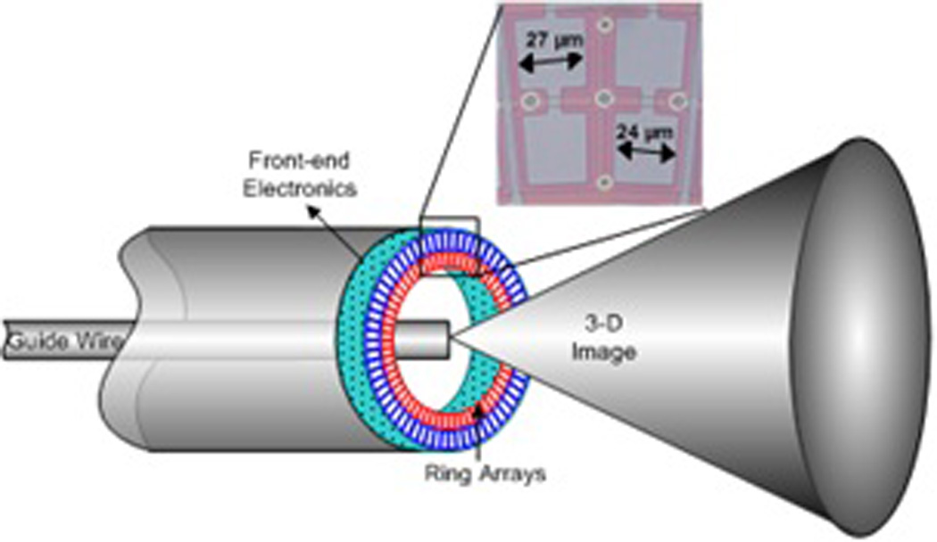
A proof of concept model of the dual-ring CMUT on CMOS catheter prototype for forward looking intravascular 3D imaging, with a zoomed in view of fabricated membranes and center guide wire.
This paper focuses on process development and evaluation for intravascular imaging applications that take greater advantage of CMUT design flexibility and monolithic integration. In particular, we consider CMOS integration with dual-ring CMUT annular arrays for forward-looking intravascular ultrasound (FL-IVUS) which have a very small element size and overall area for electronics. These arrays have been previously fabricated and tested on bulk silicon for integration with an IVUS catheter with a diameter on the order of 1 mm to 2 mm [7], [8], [9]. Direct integration with electronics not only increases the signal-to-noise (SNR) of CMUTs by decreasing parasitic capacitances but also significantly reduces the complexity of design while optimizing the use of catheter tip real estate. Estimated parasitic capacitances associated with a single Rx element up to the point of connection to an amplifier, shown in Fig. 1, are reduced by more than a factor of 200 as compared to wire bonding by monolithic integration as numerically calculated (See Table I). The TIA input capacitance, which was used in this study, was simulated to be 400 fF. For an ideal case, the electronic and CMUT design parameters should not significantly affect the other. Additionally, the process flow for the post processing of CMUTs on electronics should keep additional steps to a minimum so as to preserve the yield. We attempted to keep these considerations in mind and have chosen to have custom CMOS electronics fabricated using the commercial foundry on 200 mm (8 inch) wafers using a 0.35 µm process [10]. The CMUTs were separately optimized for monolithic integration via post processing of the CMOS wafer.
TABLE I.
Array Element Connection Capacitance
| DRA Wire Bond Connections |
DRA CMOS Connections |
|
|---|---|---|
| Receiver Element (CMUT) | 114 fF | 114 fF |
| Connection Line | 42 fF | 11 fF |
| Bond Pad | 239 fF | - |
| Wire bond | 2 pF | - |
| Total Parasitic Capacitance | 2.281 pF | 11 fF |
| Parasitic to CMUT Ratio | 20:1 | 1:11 |
Fig. 2 shows a schematic cross section of an Rx element integrated with a CMOS wafer. The bottom electrode is connected to the amplifier with a common electrode above for the application of the DC bias. Multiple Rx elements, 8 or 16 depending upon the size of the array, are multiplexed to one of four output buffers and then connected to an external transmission line. The connections to the electronics are accomplished through the use of conformal metal sputtering through sloped sidewall etching as shown at the TIA input and buffer output.
Fig. 2.
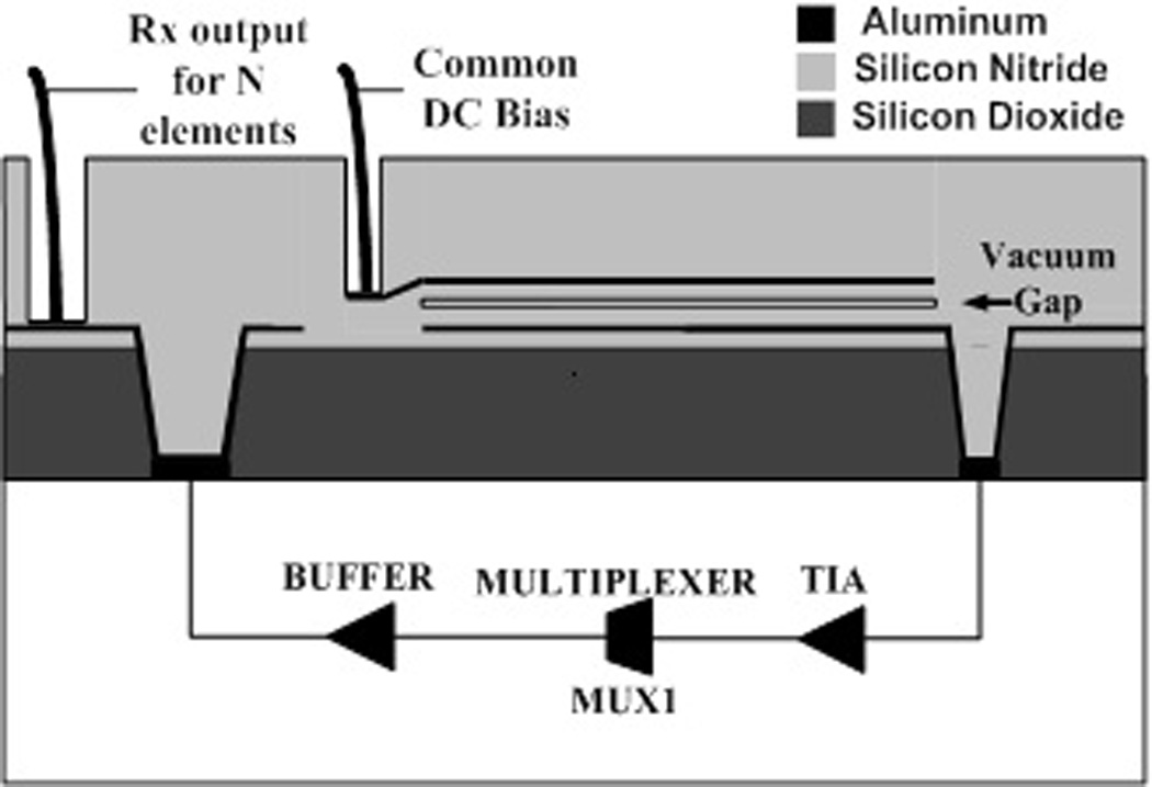
Cross-section schematic of the CMUT on CMOS membrane and the critical metal interconnections made to CMOS electronics. Receive elements are connected and divided between multiplexers for receiver output signals and all receive elements are connected to a common DC bias. Dual ring arrays use four multiplexers, MUX1-4, to route one output from a group of 8 or 16 receive channels for parallel output.
The silicon-based fabrication methods employed are ideally suited for IVUS applications and easily integrate with CMOS electronics. Well established micromachining techniques allow for densely populated 2D arrays capable of forward-looking volumetric imaging. The same transducer density necessary for volumetric imaging is difficult to achieve with current piezoelectric fabrication techniques [6].
Single and dual-ring arrays have been previously investigated and fabricated specifically for FL-IVUS applications. Here, we briefly review the literature on CMUT-electonics integration to place the current work in the proper context. We then describe the fabrication process in detail especially focusing on isolation and connection between the CMUT and CMOS layers, which are both custom designed. We then present the electrical and acoustic characterization results along with an initial volumetric imaging demonstration obtained from a 1.6 mm dual-ring CMUT on CMOS array with 15 MHz center frequency.
II. CMUT-CMOS Integration Techniques
Previous CMUT-electronics integration has been successful, but the complexity and tradeoffs of the various methods used can be significant to such a degree as to be prohibitive for particular applications. In the following subsections, we outline the main advantages and disadvantages of previously reported CMUT-electronics integration techniques.
A. CMUT in CMOS
Processing of the CMUTs can be simultaneously accomplished with the fabrication of electronics utilizing reliable and well-established CMOS processing techniques [11]. Due to the parallel processing, the overall fabrication time and processing costs are reduced. However, the design space for the CMUTs suffers from the limited CMOS fabrication options in terms of material types, material properties, and layer thicknesses. Total device area also increases as the electronics and CMUTs must be positioned side-by-side. Therefore, this is not an ideal scheme for FL-IVUS applications where available space is limited.
B. Interleaved CMUT-CMOS
To improve upon the CMUT design space, it is possible to interrupt the electronics fabrication for outside processing [12], [13]. This method has been utilized to generate smaller gap heights as compared to the aforementioned CMUT in CMOS processing. This technique increases cost and fabrication complexity and may experience resistance from commercial CMOS foundries due to contamination concerns. In addition, even though CMUT performance can be improved, this process is still similar to the standard CMUT in CMOS technique outlined above, in which available area is not optimally utilized.
C. Flip Chip Integration
To improve utilization of available device area, and to allow better optimization of CMUT material properties, separately fabricated CMOS and CMUT chips can be electrically connected through flip chip bonding [14], [15]. In this case, the CMUTs are not limited to low temperature, CMOS-compatible fabrication processes, nor are they limited to the materials and layer thicknesses designated by standardized foundry processes. However, this interconnect method requires a number of additional fabrication steps that include deep reactive ion etching, conformal metal and dielectric depositions, backside patterning, and the final wafer bonding step [16]. Furthermore, the packaging techniques associated with this technology are complex in nature adding to the overall cost. This technique is attractive for larger CMUT arrays [17], but may not be ideal for FL-IVUS applications as the minimum solder bump pitch approaches the CMUT element pitch.
D. CMUT on CMOS
This paper will outline a process in which CMUTs are fabricated directly on top of pre-processed CMOS wafers, similar to R.A Noble et al. in [18], [19] and C. Daft et al. in [20]. This interconnect approach minimizes parasitic capacitances associated with connection lines while introducing only one additional masking step. Total occupied area is minimized as the CMUTs can be located over CMOS metal layers, similar to the flip-chip bonding method, but without the complexity and spacing requirements associated with solder bump technology. In addition, the CMUTs are not constrained by the CMOS processing steps, so it is possible to optimize material properties and produce thinner vacuum gaps for low voltage operation and increased electromechanical coupling efficiency. A drawback to this method is that fabrication is limited to processes under 250 °C so as not to damage the CMOS. However, we show that the performance of CMUTs fabricated with such low temperature PECVD silicon nitride and oxide are not significantly affected.
The main the main design trade-offs associated with different CMOS integration approaches is summarized in Table II. For the design constraints associated with FL-IVUS, CMUT on CMOS fabrication was pursued as a good compromise with advantages in optimal space utilization, minimal parasitic capacitances, and relative ease of fabrication and final assembly.
TABLE II.
CMUT Integration Comparison
| CMUT in CMOS | Interleaved | Flip Chip | CMUT on CMOS | |
|---|---|---|---|---|
| Number of Processing Steps |
+ | + | − | − |
| Active CMUT Area Optimization | − | − | + | + |
| Processing Temperature | n/a | − | + | − |
| Gap Height Control | − | + | + | + |
| CMUT to CMOS Interconnect Assembly | + | + | − | + |
| Foundry Compatibility | + | − | n/a | n/a |
III. Fabrication and Processing of CMUTs on CMOS
Integration of the CMUTs with the CMOS electronics requires modification of the CMOS surface prior to CMUT fabrication, and the process flow for the CMUTs includes additional steps for electrical connections. The CMOS surface preparation, CMUT-CMOS interconnection, and subsequent processing steps are discussed in the following sections.
A. CMOS Wafers
Custom CMOS electronics were fabricated through the TSMC’s 0.35 µm processing technology on 200 mm silicon wafers with 48 repeated squares per wafer as shown in Fig. 3a. Each square contained many die with a variety of designs with multiplexers and trans-impedance amplifiers (TIAs) for the different CMUT designs. These wafers were subsequently diced yielding 6 rectangular blocks approximately 4 cm by 7 cm (3 × 2 die) to allow for CMUT fabrication using standard micromachining tools designed for 100 mm (4 inch) wafers as shown in Fig. 3b. No carrier wafers were used as the lithography tools utilized accepted rectangular samples. Due to its rectangular shape, processing uniformity is adversely affected in the upper right and lower left corners of the CMOS block as indicated in Fig. 3b. This result was attributed to the pooling of photoresist in the corners of the rectangular blocks during the photoresist spinning process.
Fig. 3.
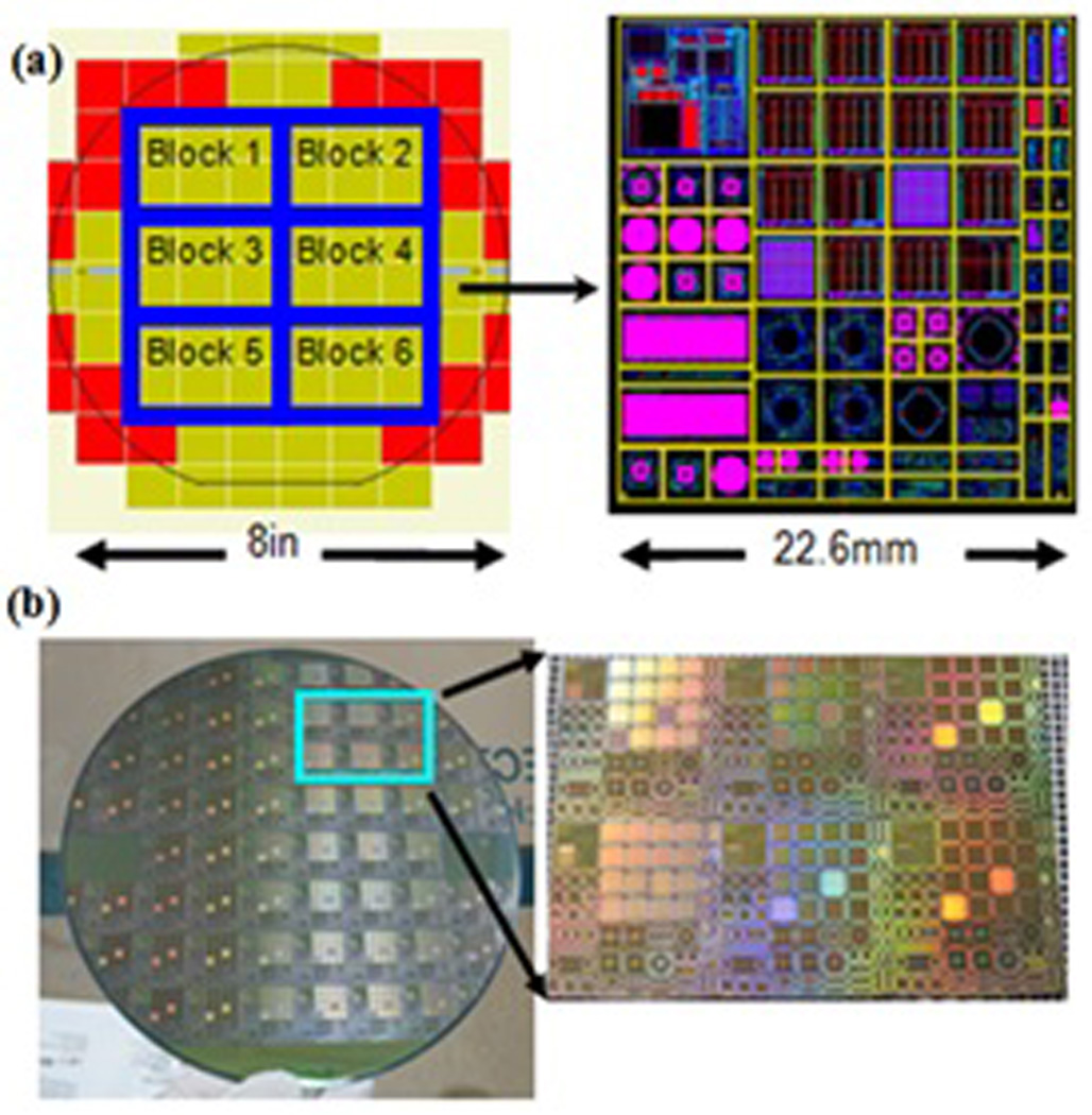
a) The repeated squares and block dicing lines are shown on the left with a magnified view of an individual square with die on the right. b) The custom 200 mm CMOS wafer is shown on the left with a diced block on the right.
Through profilometer scans, it was found that layers from the CMOS can protrude as much as 1 µm in critical regions where CMUTs are fabricated, as shown in Fig. 4a. Subsequent CMUT processing on such topography could lead to problems such as open circuitry in the CMUT metallization layers as well as non-uniformity in CMUT geometry.
Fig. 4.
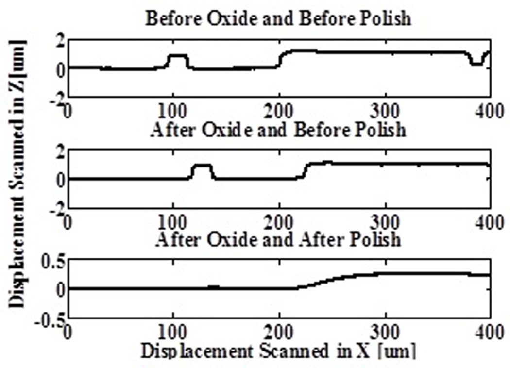
Profilometer scans of the same region shown (from top to bottom): (a) the initial topography, (b) after 3 µm of PECVD silicon dioxide passivation, (c) after 3 hours of polishing. The scan of the polished surface shows significantly reduced topography.
B. Improved CMUT on CMOS integration
1) Polishing
To address the CMOS topography, planarization through mechanical polishing was pursued. A 3 µm layer of PECVD silicon dioxide (SiO2) was deposited to electrically isolate the bottom electrodes of the CMUT devices from the CMOS electronics beneath while providing extra base surface material to be removed during polishing. Fig. 4b displays the profilometer scan of the CMOS surface taken after the oxide deposition. The oxide layer was then planarized using a Logitech PM5 automated polisher with Leeco 1 µm aluminum oxide slurry for approximately 3 hours. Profilometer scans showed that the surface topography had been significantly reduced, and all previously observed steep slopes had been polished down to very gradual inclines of less than 0.5 degrees from the horizontal (see Fig. 4c). Residual slurry contamination from the polishing process was removed in an ultrasonic cleaner in acetone and if necessary, a dip in Aluminum Etch Type A which attacks aluminum oxide but not the SiO2 layer. Further surface preparation included 0.2 µm of PECVD silicon nitride deposition after polishing to improve stiction with the first aluminum layer in the CMUT process which also forms bond pad regions. In previous fabrication, the bottom electrode metal layer would often delaminate from the polished oxide surface during wire bonding. This new approach improved the wire bond success rate from approximately 10% to near 100%. The silicon nitride addition was preferred to oxide as previous testing revealed that it exhibited better bondpad adhesion, while etching twice as fast as oxide in subsequent processing (see Table III).
TABLE III.
PHOTOLITHOGRAPHY & RIE ETCHING RECIPE FOR CMOS CONNECTION VIAS
| PHOTOLITHOGRAPHY | |||
|---|---|---|---|
| Photoresist SC-1827 |
Spin Rate (RPM) 2500 |
Ramp Speed (R/s) 500 |
Time (s) 40 |
| Pre-Bake Lindberg Oven |
Temperature (°C) 110 |
Time (min) 6–8 |
|
|
Exposure Karl Suss MA-6 |
UV Wavelength (nm) 405 |
Dose (mJ/cm2) 250–300 |
|
| Developer MF-319 |
Time (s) 110–120 |
Agitation yes |
|
| RIE ETCHING | |||
| Etch Material PECVD SiO2 |
RF Power (W) 300 |
Pressure (mTorr) 22 |
|
| CHF3 (SCCM) 40 |
O2 (SCCM) 6 |
Etch Rate (Å/min) 300 |
|
2) CMUT Connections to CMOS Electronics
We have previously reported on an interconnect scheme that uses sloped sidewall vias with conformal metal sputtering. This method is simple, only introducing one fabrication mask, [21] and uses the Advanced Vacuum Vision 320 reactive ion etch (RIE) with a modified recipe to produce sloped side walls (see Table III). Scanning electron microscope images in Fig. 5 show the side wall profile of 3 µm diameter test vias.
Fig. 5.
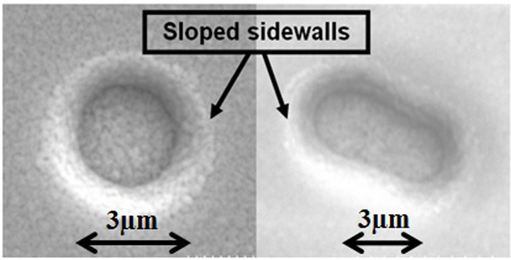
SEM pictures of 3 µm connection vias through silicon dioxide showing sloped side walls from the modified RIE recipe.
Due to the rectangular shape of the samples, spun-on photoresists collect at opposing corners forming a thicker region and in crevices formed by the remaining CMOS topography. Therefore it was necessary to over expose and over develop to ensure proper via opening across the entire sample. Aluminum metal connections in the CMOS layer act as an etch stop for the RIE process preventing over etching of the isolation layer. Table III outlines the detailed CMOS interconnect fabrication process parameters.
Electrical tests were performed with point probes verifying the continuity through two vias with deposited aluminum bond pads connected through a metal CMOS layer. The thickness of the metal trace on the CMOS layer was not known, but with a width of 25 µm and utilizing all metal layers, it was assumed that the internal resistance of the trace would be small. A total resistance on the order of 10 ohms was measured across multiple samples indicating electrical connections were established through two separate vias simultaneously.
C. Post CMOS Fabrication of CMUTs
Further CMUT processing follows well defined recipes described in J.Knight et al. [22] and details are omitted here. Dimensions for the layer thicknesses can be found in Table IV. In all lithography steps following the opening of the CMOS connections, Shipley 1813 was used instead of Shipley 1827 with similar over exposure and development. The thinner photoresist coupled with increased exposure and development helped to prevent residual photoresist from collecting in the crevices of the remaining CMOS topography and preventing shorting of the metal layers. Some of the finer features of the CMUTs suffer from the over-developing in that the sharp corners of the square areas became slightly rounded similar to a chamfered corner. However, testing indicated no significant adverse effects to CMUT performance.
TABLE IV.
TYPICAL CMUT THICKNESS DIMENSIONS
| Layer | Thickness |
|---|---|
| SiO2 planarization layer (before polishing) | 3 µm |
| Nitride layer for stiction improvement | 0.2 µm |
| Bottom and top electrode (Al / Cr) | 0.12 µm / 0.02 µm |
| Nitride isolation layers (x2) | 0.2 µm |
| Chromium sacrificial layer | 0.12 µm |
| Nitride membrane thickness | 1.5 – 3 µm |
With the aid of in-house polishing, improved CMOS connection vias, and photolithography modifications, we have successfully integrated different CMUT arrays with custom CMOS electronics for intravascular ultrasound applications. Fig. 6 shows two examples of these arrays. The 1.6 mm diameter dual-ring FL-IVUS array on the left consists of 64 receiver elements on the outer ring and 24 transmitters in the inner ring. The CMOS electronics contain one transimpedance amplifier (TIA) for each receiver, and four 16×1 multiplexers to route 4 receiver channels to the 4 output buffers. The electronics also include the digital decoding and control lines to collect data in a sequential manner from all transmit-receive combinations. In this version of the electronics the transmitters are driven by outside pulsers, but are being integrated into the same chip in future versions. In the FL-IVUS array shown in Fig. 6 (a), the electronics are not located directly beneath the CMUTs as this was a proof of concept design. Concurrently, other FL-IVUS arrays with smaller dimensions were also fabricated with electronics directly below CMUT arrays without complication, Fig. 6 (b). These devices have Tx elements connected to external bond pads for wire bonding and testing purposes.
Fig. 6.
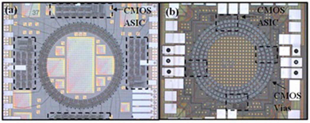
a) A fully fabricated CMUT on CMOS dual ring array with a 1.6 mm diameter array b) a 840 µm diameter array fabricated directly on top of the CMOS ASIC for FL-IVUS application.
D. CMOS-CMUT Specific Design Issues
During the design phase of the CMOS electronics and associated CMUT masks, certain considerations were kept in mind to ensure reliable integration. First, alignment marks in the shape of crosshairs, were included in the CMOS metal layers that could be observed on the finished electronics for CMUT mask alignment. Secondly, the CMOS electronic connection studs where the CMUT connects to the associated electronic input were defined to be on the top metal layer. The studs were larger than the connection etch holes to act as an etch stop during the via opening so that other CMOS layers would not be accidentally etched. The stud and via locations were placed to the sides of the CMUTs as it introduced topography on the order of microns. If the CMUT membrane were to be directly above a via, it could interfere with the membrane performance. The CMUT mask for the metal layer following the via etching, which connected the CMUTs to the electronics, masked the entire via location with ~25% additional coverage to prevent accidental etching of the metal studs if misaligned. As mentioned previously, all processing steps were limited to temperatures no greater 250 °C, so as not to adversely affect the CMOS electronics. Outside of these considerations, standard CMOS and CMUT design rules were adhered to. Finally, the SiO2 isolation layer thickness should be greater than 1 µm to ensure that there is no dielectric breakdown between the high voltage (100–200 V) bias lines and the underlying low voltage CMOS and ground lines.
IV. Experimental Characterization
For electrical and acoustical characterization of the CMUT on CMOS devices, the dual-ring FL-IVUS array shown in Fig. 6a was used since this array has larger area and larger number of array elements than the other FL-IVUS arrays concurrently fabricated. Each element consists of 4 rectangular CMUT membranes as seen in Fig 1. As shown, there are two different sized membranes that are electrically connected to form each element. The motivation behind this design was to maximize the active transducer area in the circular transducer region available. Smaller ring arrays for FL-IVUS with CMOS directly beneath CMUTs (shown in Fig. 6b) have also been successfully tested as reported in G. Gurun et al. [23], but those were designed with fewer elements and were not as ideal to demonstrate volumetric imaging in this frequency range.
Due to the small membrane sizes and the number of Tx and Rx elements, it is possible for misalignment and process variation to decrease the uniformity across an array. As a figure of merit, we investigated the uniformity of a CMUT on CMOS array as well as an array with identical mask design fabricated on a standard silicon wafer for comparison. Additional experimental characterization included pulse echo experiments to evaluate the frequency response and finally initial volumetric images obtained by the FL-IVUS arrays.
A. Electrical Characterization
To characterize uniformity, a CMUT on CMOS FL-IVUS array was attached to a custom PCB with each of the 24 Tx CMUT elements wirebonded to a separate connection pad. An Agilent 8753ES network analyzer was used to measure the resonant frequency of the Tx elements at 70 V DC bias, well below the average collapse voltage of 96 V. It was not possible to directly test the Rx elements as they were only connected to the CMOS with no external testing connections. Testing in air is beneficial for uniformity characterization as the differences in resonances are more apparent with the higher quality factor as opposed to operation in a fluid medium. Because of the two different membrane sizes within a CMUT element, two distinct resonance peaks are seen in the real part of the electrical impedance for a single Tx element as shown in Fig. 7. For uniformity evaluation, impedance data were collected for each Tx element of the integrated CMUT on CMOS dual-ring array. The two distinct resonant peak frequencies for each Tx element across the 24 element array were measured with average resonances calculated as 13.7 MHz and 16.7 MHz. Numerical methods based on a thin plate approximation and a finite difference method [24] were used to calculate the resonances in air of the two different sized membranes which were found to be 13.7 MHz and 16.7 MHz, in excellent agreement with measurements. The percent difference for each Tx element from the average resonance frequency does not exceed 6% implying acceptable uniformity from the fabrication. Most of this variation is likely due to the pre-process polishing and geometrical variation introduced while working with rectangular CMOS samples including the associated misalignment errors. Any non-uniformity in mechanical behavior due to the PECVD nitride depositions should be minimal considering a given device occupies such a relatively small space on the wafer.
Fig. 7.
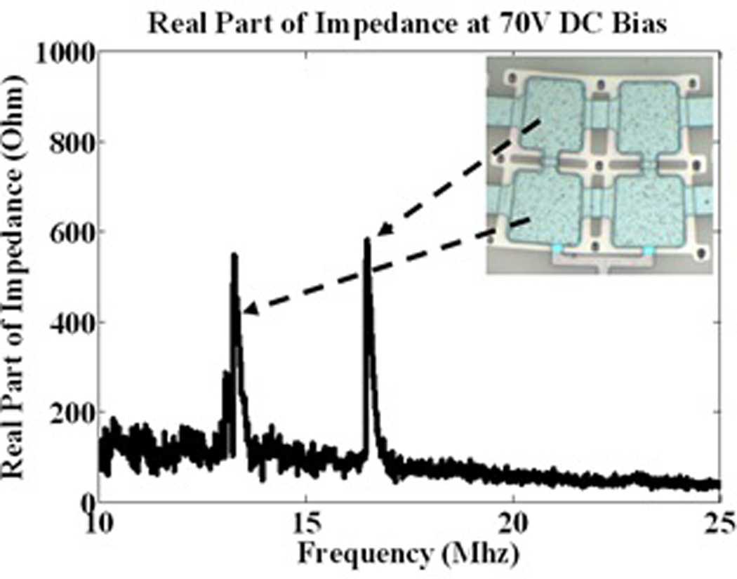
Agilent network analyzer measurement of real electrical impedance reflected from fabricated CMUT on CMOS device showing 2 distinct resonant peaks due to membrane geometry differences. The peaks of this transmitter are measured at 13.3 MHz and 16.5 MHz
Similar data were obtained on CMUT arrays fabricated on a blank 100 mm silicon wafer using the CMUT on CMOS mask set. The resonances in air were measured to be on average 14.7 MHz and 17.1 MHz with the percent difference of each Tx element not exceeding 6%. The calculated resonances were 14.4 MHz and 17.2 MHz. The higher resonances are attributed to a slight increase in the membrane thickness, ~ 0.1 µm, which occurred during fabrication. This indicates that the CMUT on CMOS fabrication techniques implemented do not significantly affect uniformity of the CMUT operation from element to element. It should be noted that in a more recent CMUT on CMOS fabrication, with better alignment and reduced surface roughness from improved polishing and optimized metal depositions, uniformity was measured to be within 1.5% of the mean. This validates the assumption that PECVD nitride should exhibit minimal variation over the elements of a single device.
B. Acoustic Characterization
A completed 1.6 mm diameter CMUT on CMOS array, as shown in Fig. 8, was wire bonded in a ceramic dual inline package (DIP, Spectrum CSB04075) and coated with 3 µm of Parylene C for electrical isolation in water. A 60 mm diameter, 15 mm tall polystyrene Petri dish was modified by milling a square opening in the base and then using epoxy to attach it to the ceramic DIP. This formed a cavity that could then be filled with water. External pulsers were connected to the Tx elements and the reflections from the air-water interface were received by Rx elements integrated with CMOS amplifiers and multiplexers. The DC bias for the Tx and Rx elements was set to 80 V, below the typical 95% of collapse voltage to avoid premature failure. A sample pulse echo signal from water-air interface at 5 mm is shown in Fig. 9 with the corresponding frequency response which was filtered from 5–30 MHz during post processing. The center frequency of the array elements is around 15 MHz as desired. There are significant spurious features in the frequency response including a dip at 7.5 MHz which is due to standing waves in the 550 µm thick silicon substrate [25], [26]. Acoustic crosstalk in the array resulting from the initial transmit pulse is also significant and corrupts the echo signal with features occurring before the target echo signal. This issue needs to be considered in the future designs with realistic donut shaped geometries, but for the purposes of this paper the pulse echo response shows that the signal levels from single Tx-Rx pairs are strong and uniform. The standard deviation in the pulse echo peak to peak amplitudes was 1.3 dB, when the output for all active receiver elements were analyzed while using the same single transmitter. A simple geometric analysis of the Tx-Rx distance combinations shows that the difference in the distance varies by not more than 5 % for an acceptance angle deviation less than 18 degrees from the vertical. Considering the small magnitude of these distance variations, the results from scanning all Rx channels demonstrate consistent and uniform acoustic response in the receiver side.
Fig. 8.
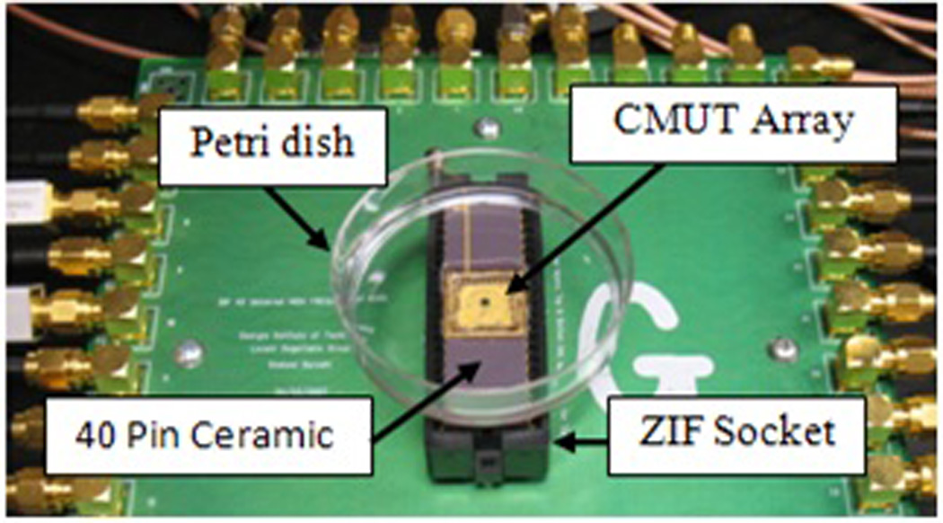
Experimental set up of wire-bonded 1.6 mm dual-ring CMUT array in a ceramic package combined with a modified Petri dish. The custom PCB board interfaces the ceramic package to external pulsers, FPGA board, high voltage bias lines, and signal output lines to the digitizer card via SMA connections.
Fig. 9.
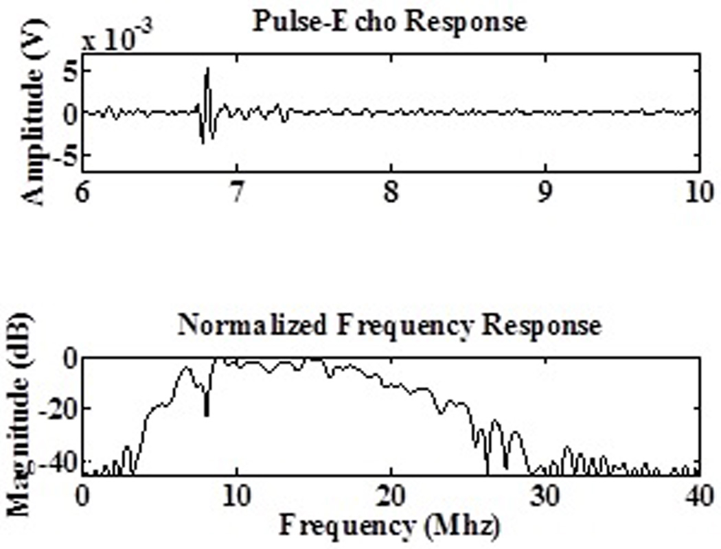
(Top) Pulse-echo response from a single pair of transmit and receive elements, showing functioning CMUT on CMOS array element. (Bottom) Frequency response from a dual ring array element in water shows that the CMUT on CMOS fabrication was successful and frequency response has enough bandwidth for imaging capabilities.
To have an estimate of the achievable pulse echo SNR, the receive bias was increased to 86 V, the water-air interface distance was set to 1 cm and the Tx element was driven with a 160 Vpp bipolar pulse centered at 15 MHz. The resultant SNR was calculated to be 41 dB using the RMS value of the received pulse divided by the RMS of the received signal without transmission, i.e. background CMOS electronic noise. The measurement bandwidth was 40 MHz, limited by the CMOS amplifiers. To evaluate the feasibility of imaging CTOs with this SNR level, we performed a calculation including diffraction losses and attenuation in blood at 15MHz with 0.14 dB/MHz-cm frequency dependence. Considering an acoustical impedance of 1.68 MRayl for blood and reflection from a typical fat tissue with impedance of 1.33 MRayl, the SNR with 48 Tx elements and 64 Rx elements at a distance of 1 cm was calculated to be 34 dB SNR, suitable for detecting CTOs in front of a catheter [27]. Simulations and measurements on a noise optimized TIA implemented in CMUT on CMOS shows that the SNR can be further improved by 15 dB [23].
To demonstrate that real time imaging data can be acquired with the FL-IVUS dual ring arrays, a custom data collection setup was constructed. It consisted of a custom high voltage pulser board to actuate the Tx elements, an FPGA board (Xilinx Virtex 5) for Tx element selection and multiplexing of the on-chip Rx elements, and a PC with 2 digitizer cards (UltraFast M3i.4142) for data collection and storage. The synthetic phased array method was used for image processing. The pulse-echo data for every Tx-Rx element pair were acquired for 20 µs (~1.5 cm imaging depth) without any time gain compensation or averaging. This results in a real time data acquisition rate of 130 frames/s considering 1536 Tx-Rx combinations and 4 parallel receive channels, which is suitable for FL-IVUS imaging. Delay and sum algorithms are then used to create a volumetric images using synthetic phased array image reconstruction. A more detailed description of the imaging setup with sample images can be found in [28].
V. Conclusions
In this paper we have described an improved fabrication process for monolithic CMUT on CMOS integration with minimal additional processing. The surface preparation of the custom CMOS electronics wafers has been shown to significantly reduce the surface topography and improve the bond pad metal stiction, yielding near perfect wirebond success.
The sloped sidewall vias have been shown to be a simple but reliable method for integrating CMUTs with CMOS electronics while minimizing the parasitic capacitances.
We have successfully fabricated and tested dual-ring arrays for FL-IVUS applications. Experimental uniformity characterization shows that CMUT performance has not been altered significantly by the improved fabrication process and is comparable to CMUTs processed on standard silicon wafers. Initial real time data collection experiments at 100 frames/s data rate was performed using a custom designed setup. The pulse echo data from array elements show that both Tx and Rx elements are functional and successful integration with CMOS electronics yields SNR levels suitable for volumetric images of tissue like reflectors in blood over 1 cm imaging depth. With proper electrical interconnect and integration to catheters, the single chip, CMUT on CMOS approach appears to be a promising technology for challenging volumetric intravascular imaging applications.
References
- 1.Ito S, et al. Novel technique using intravascular ultrasound-guided guidewire cross in coronary intervention for uncrossable chronic total occlusions. Circulation Journal. 2004;68(11):1088–1092. doi: 10.1253/circj.68.1088. [DOI] [PubMed] [Google Scholar]
- 2.Courtney BK, et al. Innovations in imaging for chronic total occlusions: a glimpse into the future of angiography’s blind-spot. European Heart Journal. 2008;29(5):583–593. doi: 10.1093/eurheartj/ehm634. [DOI] [PubMed] [Google Scholar]
- 3.Yock PG, Fitzgerald PJ. Intravascular ultrasound: state of the art and future directions. American Journal Cardiology. 1998;vol. 81(7A):27532E. doi: 10.1016/s0002-9149(98)00195-7. [DOI] [PubMed] [Google Scholar]
- 4.Honda Y, Fitzgerald PJ. Frontiers in Intravascular Imaging Technologies. Circulation Journal. 2008;117(15):2024–2037. doi: 10.1161/CIRCULATIONAHA.105.551804. [DOI] [PubMed] [Google Scholar]
- 5.Soon KH, Selvanayagam JB, Cox N, Kelly A, Bell KW, Lim YL. Percutaneous revascularization of chronic total occulusions: Review of the role of invasive and non-invasive imaging modalities. International Journal of Cardiology. 2007;116:1–6. doi: 10.1016/j.ijcard.2006.03.023. [DOI] [PubMed] [Google Scholar]
- 6.Jongbloed MRM, et al. Clinical applications of intracardiac echocardiography in interventional procedures. Heart. 2005;91(7):981–990. doi: 10.1136/hrt.2004.050443. [DOI] [PMC free article] [PubMed] [Google Scholar]
- 7.Degertekin FL, Guldiken RO, Karaman M. Annular-Ring CMUT Arrays for Forward-Looking IVUS: Transducer Characterization and Imaging. IEEE transactions on ultrasonics, ferroelectrics, and frequency control. 2006;vol. 53(No. 2) doi: 10.1109/tuffc.2006.1593387. [DOI] [PubMed] [Google Scholar]
- 8.Guldiken R, Zahorian J, Balantekin M, Degeterkin FL, Tekeş C, Şişman A, Karaman M. Dual-Annular-Ring CMUT Array for Forward-Looking IVUS Imaging. IEEE Ultrasonics Symposium. 2006:698–701. [Google Scholar]
- 9.Şişman A, Zahorian J, Gürün G, Karaman M, Balantekin B, Degertekin FL, Hasler P. Evaluation of CMUT Annular Arrays for Side-looking IVUS. IEEE International Ultrasonics Symposium Proceeding. 2009:988–991. [Google Scholar]
- 10.Gurun G, Qureshi MS, Balantekin M, Guldiken R, Zahorian J, Sheng-Yu Peng, Basu A, Karaman M, Hasler P, Degertekin L. Front-end CMOS electronics for monolithic integration with CMUT arrays: Circuit design and initial experimental results. Ultrasonics Symposium, 2008. IUS 2008. IEEE. 2008 Nov.:390–393. 2–5. [Google Scholar]
- 11.Cheng X, Lemmerhirt DF, Kripfgans OD, Zhang M, Yang C, Rich CA, Fowlkes JB. CMUT-in-CMOS Ultrasonic Transducer Arrays With On-Chip Electronics. Solid-State Sensors, Actuators and Microsystem Conference, 2009. Transducers. 2009:1222–1225. [Google Scholar]
- 12.Eccardt PC, Niederer K. Micromachined ultrasound transducers with improved coupling factors from a CMOS compatible process. Ultrasonics. 2000;vol. 38:774–780. doi: 10.1016/s0041-624x(99)00085-2. [DOI] [PubMed] [Google Scholar]
- 13.Eccardt PC, Niederer K, Scheiter T, Hierold C. Surface Micromachined Ultrasound Transducers in CMOS technology. IEEE Ultrasonic Symposium. 1996:959–962. [Google Scholar]
- 14.Cheng CH, Chow EM, Jin X, Ergun S, Khuri-Yakub BT. An Efficient Electrical Addressing Method Using Through-Wafer Vias For Two-Dimensional Ultrasonic Arrays. IEEE Ultrasonics Symposium. 2000 1179-118. [Google Scholar]
- 15.Nikoozadeh A, Wygant IO, Lin D, Oralkan O, Ergun AS, Stephens DN, Tomenius KE, Dentinger AM, Wildes D, Akopyan G, Shivkumar K, Mahajan A, Sahn DJ, Khuri-Yakub BT. Forward-Looking Intracardiac Ultrasound Imaging Using a 1-D CMUT Array Integrated With Custom Front-End Electronics. IEEE Transactions on Ultrasonics, Ferroelectrics, and Frequency Control. 2008 Dec;vol. 55(No. 12) doi: 10.1109/TUFFC.2008.980. [DOI] [PMC free article] [PubMed] [Google Scholar]
- 16.Wygant IO, Zhuang X, Yeh DT, Oralkan O, Ergun AS, Karaman M, Khuri-Yakub BT. integration of 2D CMUT Arrays with Front-End Electronics for Volumetric Ultrasound Imaging. IEEE transaction on ultrasonics, ferroelectrics, and frequency control. 2008 Feb;vol. 55(No. 2) doi: 10.1109/TUFFC.2008.652. [DOI] [PubMed] [Google Scholar]
- 17.Nikoozadeh A, Oralkan O, Gencel M, Choe JW, Stephens DN, Rama A, Chen P, Lin F, Dentinger A, Wildes D, Thomenius K, Shivkumar K, Mahajan A, Seo CH, O’Donnel M, Truong U, Sahn DJ, Khuri-Yakub PT. Forward-Looking Intracardiac Imaging Catheters Using Fully Integrated CMUT Arrays. Ultrasonics Symposium. 2010 Oct. doi: 10.1109/IEMBS.2010.5627580. IUS 2010. [DOI] [PMC free article] [PubMed] [Google Scholar]
- 18.Noble RA, Davies RR, Day MM, Koker L, King DO, Brunson KM, Jones ARD, McIntosh JS, Hutchins DA, Robertson TJ, Saul P. A Cost-effective and Manufacturable Route to the Fabraication of High-Density 2D Micromachined Ultrasonic Transducer Arrays and (CMOS) Signal Conditioning Electronics on the same Silicon Substrate. IEEE Ultrasonics Symposium. 2001:941–945. [Google Scholar]
- 19.Noble RA, Davies RR, King DO, Day MM, Jones ARD, McIntosh JS, Hutchins DA, Saul P. Low-Temperature Micromachined cMUTs with Fully-Integrated Analogue Front-End Electronics. IEEE Ultrasonics Symposium. 2002:1045–1055. [Google Scholar]
- 20.Daft C, Calmes S, Graca D, Patel K, Wagner P, Ladabaum I. Microfabricated Ultrasonic Transducers Monolithically Integrated with High Voltage Electronics. IEEE Ultrasonics Symposium. 2004:493–496. [Google Scholar]
- 21.Zahorian J, Guldiken R, Gurun G, Qureshi MS, Balantekin M, Hasler P, Degertekin FL. Single chip CMUT arrays with integrated CMOS electronics: Fabrication Process Development and Experimental Results. IEEE International Ultrasonics Symposium Proceedings. 2008:386–389. [Google Scholar]
- 22.Knight J, McLean J, Degertekin FL. Low temperature fabrication of immersion capacitive micromachined ultrasonic transducers on silicon and dielectric substrates. IEEE Trans. Ultrasounics, Ferroelectric, and Frequency Control. 2004;vol. 51(No.10):1324–1333. [Google Scholar]
- 23.Gurun G, Hasler P, Degertekin FL. Frontend Receiver Electronics for High Frequency Monolithic CMUT-on-CMOS Imaging Arrays. Ultrasonics, Ferroelectrics and Frequency Control, IEEE Transactions on. 2011:1658–1668. doi: 10.1109/TUFFC.2011.1993. [DOI] [PMC free article] [PubMed] [Google Scholar]
- 24.Meynier C, Franck Teston, Dominique Certon A multiscale model for array of capacitive micromachined ultrasonic transducers. J. Acoust. Soc. Am. 2010;vol. 128:2549–2561. doi: 10.1121/1.3493433. [DOI] [PubMed] [Google Scholar]
- 25.Guldiken RO, Zahorian J, Yamaner F, Degertekin FL. Dual-electrode CMUT with non-uniform membranes for high electromechanical coupling coefficient and high bandwidth operation. Ultrasonics, Ferroelectrics and Frequency Control, IEEE Transactions on. 2009 Jun;vol.56(no.6):1270–1276. doi: 10.1109/TUFFC.2009.1169. [DOI] [PMC free article] [PubMed] [Google Scholar]
- 26.Ladabaum I, Wagner P, Zanelli C, Mould J, Reynolds P, Wojcik G. Silicon substrate ringing in microfabricated ultrasonic transducers. Ultrasonics Symposium, 2000 IEEE. 2000 Oct;vol.1:943–946. no. [Google Scholar]
- 27.Szabo T. Diagnostic Ultrasound Imaging: Inside out, 1st ed. Burlington, USA: Elsevier Academic Press; 2004. Appendix B; p. 535. Appedix B. [Google Scholar]
- 28.Hochman M, Zahorian J, Satir S, Gurun G, Xu T, Karaman M, Hasler P, Degertekin FL. CMUT-on-CMOS for Forward-Looking IVUS: Improved Fabrication and Real-Time Imaging. Ultrasonics Symposium. 2010 Oct; IUS 2010. [Google Scholar]


