Abstract
This paper describes the design of a front-end circuit consisting of an integrated preamplifier with a Sallen-Key Butterworth filter for very-high-frequency ultrasonic transducers and a low-power handheld receiver. This preamplifier was fabricated using a 0.18-μm 7WL SiGe bi-polar complementary metal oxide semiconductor (BiCMOS) process. The Sallen-Key filter is used to increase the voltage gain of the front-end circuit for high-frequency transducers which are generally low in sensitivity. The measured peak voltage gain of the frontend circuits for the BiCMOS preamplifier with the Sallen-Key filter was 41.28 dB at 100 MHz with a −6-dB bandwidth of 91%, and the dc power consumption of the BiCMOS preamplifier was 49.53 mW. The peak voltage gain of the front-end circuits for the CMOS preamplifier with the Sallen-Key filter was 39.52 dB at 100 MHz with a −6-dB bandwidth of 108%, and the dc power consumption of the CMOS preamplifier was 43.57 mW. Pulse-echo responses and wire phantom images with a single-element ultrasonic transducer have been acquired to demonstrate the performance of the front-end circuit.
I. Introduction
Ultrasound imaging systems at higher frequency (>20 M Hz) have better spatial resolution for many medical imaging applications than those at lower frequency (a few hertz to 15 M Hz) [1], [2]. The first stage of the receiver unit in an ultrasonic imaging system usually contains a preamplifier and a filter, which can affect the performance of the system to a significant degree. The design of a high-frequency front-end circuit which can be integrated into a receiving channel of an array is a challenge [3]. First, electrical impedance matching is one of the important issues, especially for very-high-frequency ultrasound preamplifiers because the performances of these preamplifiers are limited by parasitic impedances of the transistors, discrete components, and chip pad as the frequency increases [3]. Second, cable loss is another issue of concern for integrated preamplifier design. Cable loss may be reduced by connecting the integrated preamplifiers as closely to the transducer as possible. Third, integrated preamplifiers must be implemented in the multi-channel format to reduce the footprint size of the layout. Fourth, multi-channel preamplifiers consume more dc power than single-channel preamplifiers, limiting the battery life of a handheld receiver.
Operational amplifiers have been widely used for frontend preamplifier design of an ultrasonic receiver. However, the gain for these devices is high in the low-frequency region but the bandwidth is limited, as shown in Figs. 1 and 2. To extend the bandwidth in the frequency domain, a feedback loop consisting of resistors and capacitors may be used [4]. However, this may lead to oscillation of the preamplifier and generate higher thermal noise [4]. Matching or optimization of the performances with additional components could be difficult because of the high input impedance of an operational amplifier.
Fig. 1.
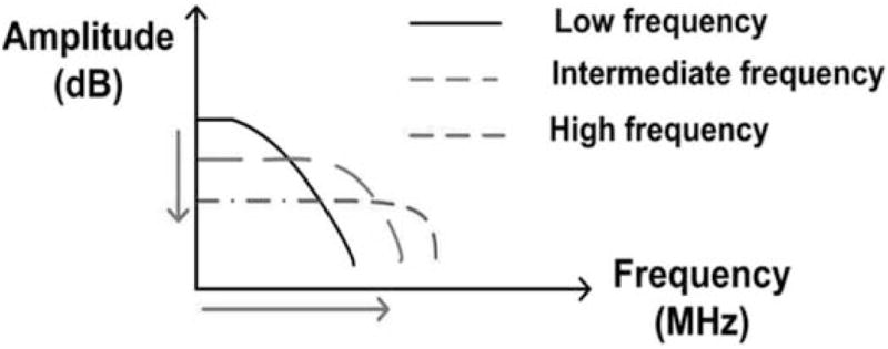
Change in voltage gain of the operational amplifier with operating frequency.
Fig. 2.
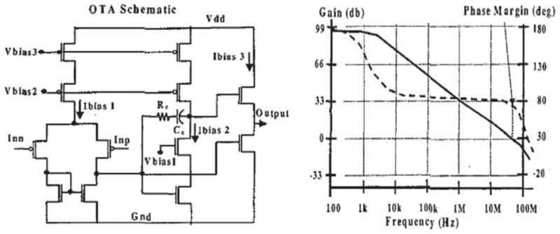
Schematic of operational preamplifier for ultrasound transducer from Morizio [5].
To overcome these problems, a novel integrated preamplifier has been designed and fabricated. By comparing CMOS and bi-polar complementary metal oxide semiconductor (BiCMOS) devices, one can provide design guidelines for the optimal performance of the integrated preamplifier for high-frequency ultrasonic transducers. CMOS and BiCMOS device characteristics are summarized in Table I. This data comparison is collected from literature and IBM technology documents [6]–[8].
TABLE I.
The Off-Chip Component Values for BiCMOS Preamplifier.
| Component | Category | Value |
|---|---|---|
| Ccap | dc coupling capacitor | 25 pF |
| Lg | Gate inductor | 200 nH |
| Cd1 | Load capacitor | 12 pF |
| Ld1 | Load inductor | 120 nH |
| Rd1 | Load resistor | 20 Ω |
| Ld2 | Load inductor | 120 nH |
| Rd2 | Load resistor | 20 Ω |
| Cout | dc coupling capacitor | 30 pF |
This design has been shown to have wider bandwidth and higher gain even for high-frequency operations because its performance can be controlled by off-chip resonant tank circuits, as shown in Fig. 3, which are a more stable architecture without a feedback loop. Impedance matching is achievable with off-chip inductors and capacitors, equivalent capacitances of the electrostatic discharge devices, and capacitance of the transistor. With this topology, the input impedance, frequency, and bandwidth can be tuned and optimized for the best performance.
Fig. 3.
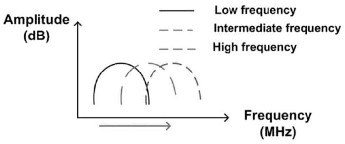
Change in voltage gain of the BiCMOS preamplifier with operating frequency.
One of the important issues of multi-channel integrated preamplifiers is dc power consumption. Operating at a higher frequency consumes more power because a preamplifier working for a higher center frequency occupies a wider bandwidth than the preamplifier at a lower center frequency. This novel preamplifier uses fewer transistors and lower values of resistances than operational amplifiers, thus generating a lower noise figure and requiring less power consumption.
II. Architecture, Design, and Fabrication
This first prototype chip contains eight BiCMOS and CMOS preamplifiers for the purpose of comparing the performances of both integrated preamplifiers. A block diagram of the integrated preamplifier with an active Sallen-Key Butterworth low-pass filter is shown in Fig. 4.
Fig. 4.

The architecture of a preamplifier with Sallen-Key Butterworth filter.
The common-source and common-gate amplifier are two commonly used low-noise amplifier topologies. For a common-gate amplifier, there is no gate-drain capacitance in the transistor (M1), providing better reverse isolation, but it inherently has a worse noise performance than a common-source topology. However, the common-source amplifier can use cascade structures to reduce the isolation, improving the stability of the circuit. Therefore, the common-source topology with a cascade structure is preferred over the common-gate with a cascade structure for better noise performance.
The source-degenerated integrated preamplifier (Fig. 5) is a viable alternative to operational amplifiers because it has more optimal impedance matching, higher operating frequency, and lower dc power consumption [6]. An analysis of the source-degenerated integrated preamplifier is described subsequently.
Fig. 5.
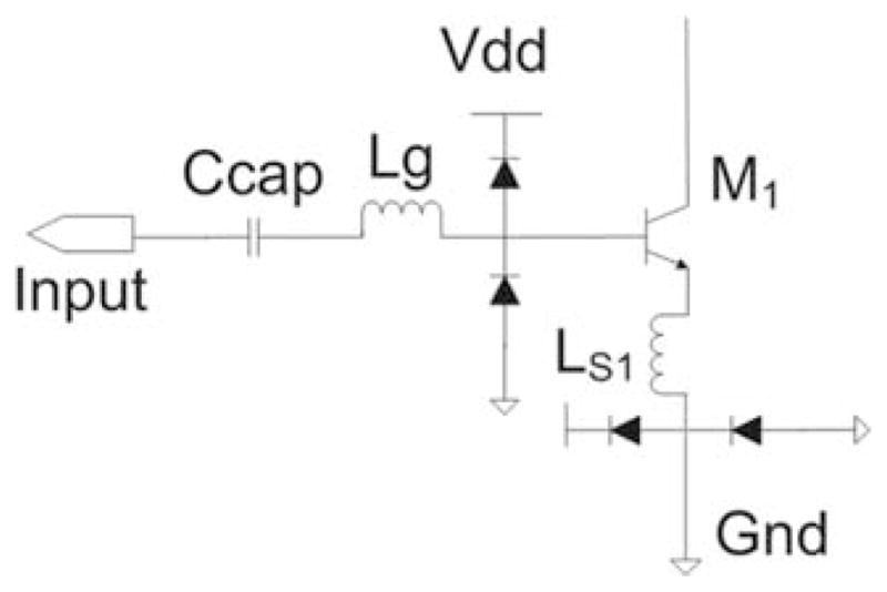
Input part of the source-degenerated integrated preamplifier.
The input impedance of the source-degenerated integrated preamplifier is defined as
| (1) |
where Ztr is the input impedance of the preamplifier, Ccap is the de-coupling capacitor, Lg is the gate inductance of the transistor M1, CESD is the total capacitance of varactor diodes, Ls1 is the source inductance of the transistor M1, gm1 is the small signal transconductance of the transistor M1, and Cπ1 is the parasitic base-emitter capacitance of the transistor M1.
With this topology, the imaginary term of (1) should be zero to match 50-Ω resistance. Although the reactive part of the impedance of an ultrasonic transducer at resonance has often been approximated as a capacitor such that a long cable or an inductor may be used to match the impedance of the receiving electronics, the equivalent circuit of the input impedance of an ultrasonic transducer over the whole bandwidth is actually a fairly complex network consisting of resistive, inductive, and capacitive components.
A. BiCMOS Preamplifier
The architecture of a BiCMOS integrated preamplifier is shown in Fig. 6. All chip pads are protected by hyperabrupt varactors for electrostatic discharge (ESD) protection devices [9].
Fig. 6.
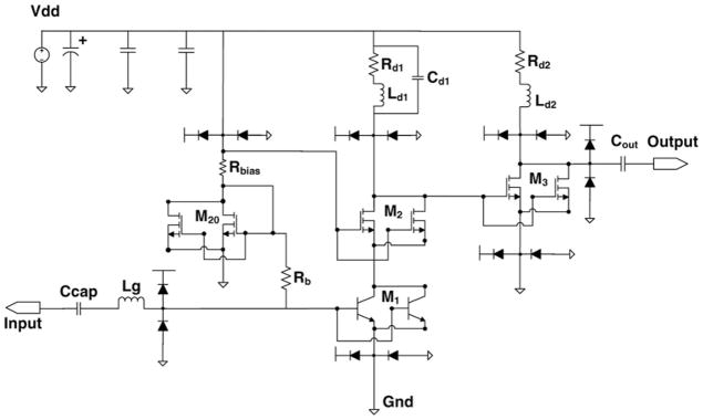
Architecture of a BiCMOS integrated preamplifier.
A new approach is needed for impedance matching for high-frequency ultrasonic transducers/arrays. If there is no source inductor, the input impedance (1) can be simplified to
| (2) |
Eq. (2) shows that electrical impedance matching with the high-frequency ultrasonic transducer can be determined by de-coupling capacitance, off-chip inductance, the equivalent capacitance of the hyperabrupt varactors and the inner capacitances of the transistor M1. Therefore, this allows us to have a means to manipulate the matching condition for the transducer more accurately and help optimize the performance of the integrated preamplifier.
The large signal transductance of the first-stage preamplifier can be replaced by
| (3) |
where gm1HBT is the small signal transconductance of the HBT(M1), iout1 is the drain current of transistor M1, and Vin1 is the gate voltage of transistor M1.
Therefore, the voltage gain of the first-stage preamplifier can be represented as
| (4) |
where gm2MOS is the small-signal transconductance of M2, Rd1 is the load resistance and inner resistance of the transistor M2, Ld1 is the load inductance, Cd1 is the load capacitance and inner capacitance of the transistor M2, and Zd1 is the load impedance of the first-stage preamplifier.
The voltage gain of the second-stage preamplifier is defined as
| (5) |
where gm3MOS is the transconductance of the MOSFET M3, Rd2 is the load resistance with inner resistance of the first- and second-stage preamplifier, and Ld2 is load inductance of the first- and second-stage preamplifier The voltage gain of the preamplifier is given by
| (6) |
The voltage gain can be improved by increasing the value of load impedance and transconductance, and by decreasing the value of load capacitance, gate-source capacitance of the transistor M1, and hyperabrupt varactor.
The center frequency and −3-dB bandwidth of the integrated preamplifier depend on the off-chip components and inner impedance of the first- and second-stage preamplifiers and are given by
| (7) |
| (8) |
where Wp is the resonant center frequency of the integrated preamplifier and BW is the −3-dB bandwidth of the integrated preamplifier.
For noise analysis of the preamplifier design, the flicker noise (also called the 1/f noise) and thermal noise from the transistors are usually considered. First, the flicker noise is dependent on the surface of the semiconductor devices [4], [8]. Generally, the HBT shows lower 1/f noise than MOSFETs because the flicker noise of the HBT is attributed to the base-emitter junction current in the substrate [9]. For the low-frequency operation of the preamplifier, the flicker noise is more dominant than the thermal noise. The input-referred flicker noise equation is given by
| (9) |
where K is the process-dependent constant on the order of 10−25V2F, Ae is the emitter junction area of HBT, IB is the base current of HBT, and f is the operating frequency
The flicker noise decreases as the frequency is increased. Further, transistors with larger width and length generate less 1/f noise. However, for the high-frequency preamplifier, the thermal noise is a more dominant factor than the flicker noise. Unlike flicker noise, thermal noise can be reduced by proper design, e.g., increasing transconductance (gm1HBT). For the common-gate MOSFET M2, the noise term can be neglected because of the large output impedance [10], [11]. With high gain in the first stage of the preamplifier, the noise term of the second stage can be neglected. Therefore, the noise figure of the BiCMOS preamplifier can be simplified to
| (10) |
where rb is the base resistance of the HBT.
The transconductance of HBT is theoretically higher than that of MOSFET, thus generating a lower noise figure for the BiCMOS preamplifier than for the CMOS preamplifier [8], [9].
B. CMOS Preamplifier
Compared with the architecture of the BiCMOS preamplifier, the HBT device M1 is replaced by MOSFET M1 in the CMOS preamplifier. Fig. 7 shows the architecture of a CMOS integrated preamplifier and its component values as listed in Table II.
Fig. 7.
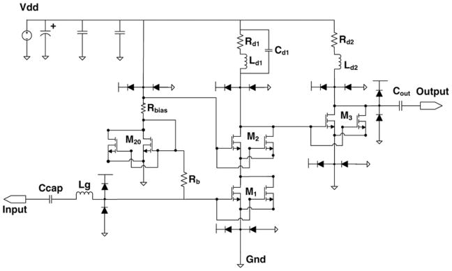
Architecture of a CMOS integrated preamplifier.
TABLE II.
The Off-Chip Component Values for CMOS Preamplifier.
| Component | Category | Value |
|---|---|---|
| Ccoup | dc coupling capacitor | 30 pF |
| Lg | Gate inductor | 150 nH |
| Cd1 | Load capacitor | 12 pF |
| Ld1 | Load inductor | 150 nH |
| RL1 | Load resistor | 20 Ω |
| Ld2 | Load inductor | 150 nH |
| RL2 | Load resistor | 20 Ω |
| Cout | dc coupling capacitor | 30 pF |
The input impedance of a CMOS preamplifier is defined as
| (11) |
where Cgs1 is the parasitic gate-source capacitance of the transistor M1.
The voltage gain of the CMOS preamplifier can be represented as
| (12) |
where gm1MOS is the transconductance of the MOSFET M1.
The noise figure of the CMOS preamplifier can be written as
| (13) |
where rg is the gate-resistance of MOSFET M1.
C. Active Sallen-Key Butterworth Filter
An active Sallen-Key Butterworth filter is used to increase the voltage gain of the front-end circuits for the high-frequency transducer. With a Sallen-Key filter topology, the high-voltage gain may affect the stability. A large capacitor (C8) is used to reject unwanted noise from the power supply [12]. The architecture of the Sallen-Key filter is shown in Fig. 8.
Fig. 8.
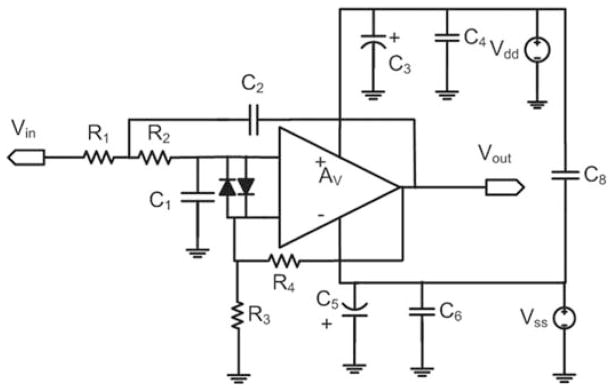
Architecture of an active Sallen-Key Butterworth low pass filter.
If the open-loop gain (Av) of the operational amplifier is infinite, the transfer function of the Sallen-Key Butterworth low pass filter can be simplified as
| (14) |
Therefore, the operational frequency (fn), open-loop gain (An), and quality factor (Q) of this active Sallen-Key Butterworth low pass filter can be represented as
| (15) |
The operational amplifier which is used for this filter is the voltage feedback amplifier (OPA843, Texas Instruments Inc., Dallas, TX).
D. Fabrication of Integrated Preamplifier
The integrated preamplifier chip was fabricated using the IBM BiCMOS 7WL process (Armonk, NY) and these preamplifiers are packaged in 40-pin dual in-line packages (DIP) from MOSIS (Marina del Rey, CA). Electrical matching is one of the most important factors to be considered in the design of an integrated preamplifier for high-frequency ultrasonic transducers. In the chip layout, mismatched circumstances are usually caused by gradient effects, which can be compensated by using multiple fingers and adjusting the length size of the transistor [13]– [14]. Simulation results show that transistor devices having two fingers yield the optimal performance.
Another important issue in the layout is the noise. Noise source reduction from transistor substrate coupling is needed. Therefore, shielding rings like substrate rings for integrated preamplifiers are used to reduce the substrate noise [14]. The connection between the ESD devices and PADS should be as short as possible to reduce the parasitic capacitances. These ESD devices are capable of protecting the preamplifiers from abrupt short pulses within a few nanoseconds. All input and output pins are connected to hyperabrupt varactors because high voltages are typically used to excite ultrasonic transducers [9], [15]. A microphotograph of the top-layout is shown in Fig 9.
Fig. 9.
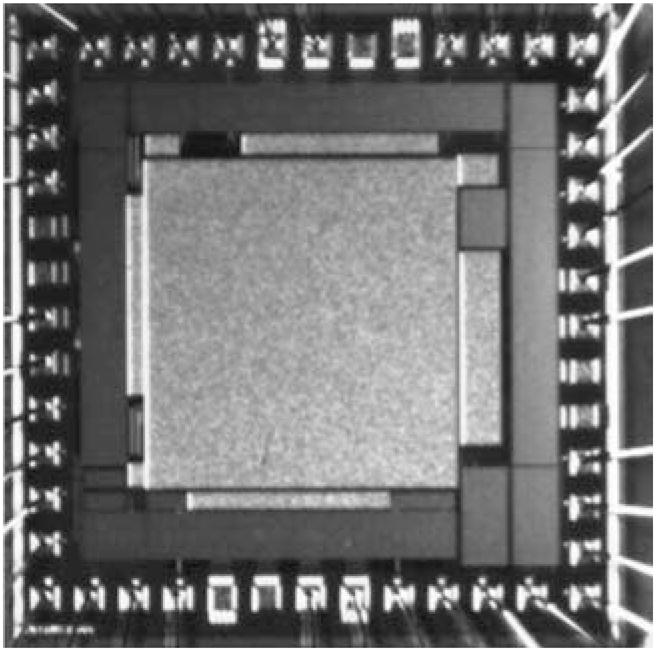
Microphotograph of the preamplifier chip.
III. Experimental Results
A. Measurement Procedure of Integrated Preamplifier and Front-End Circuits
Each of the selected preamplifiers with an active Sallen-Key Butterworth low-pass filter was measured and tested with a lithium niobate (LiNbO3) ultrasonic transducer to obtain the pulse-echo responses and wire phantom images. The S-parameters are useful performance indicators of circuits or systems because other parameters are technically more difficult to measure at high frequencies. The S-parameters (gain, input and output reflection coefficient, and noise figure), the input third-order intercept point (IIP3), the output 1-dB output compression point (P1dB), and the output third-order intercept point (OIP3) of the integrated preamplifier with the gain of the front-end circuit were measured. Impedance matching conditions can be described with input reflection coefficient (S11) and output reflection coefficient (S22), swept from 20 to 240 M Hz, and they should be below −10 dB for the desired center frequency. The reverse gain (S12) is the reverse isolation from the output port to the input port. A low value of S12 shows good isolation in the circuit.
The noise figure measurements were carried out with a spectrum analyzer (EE4401B, Agilent Technologies, Santa Clara, CA) and a high-gain amplifier (AU-1114, MITEQ, Hauppauge, NY). For noise figure measurements, the gain method was used [16], [17]. This method requires a high gain to measure the performance. Because the gain of integrated preamplifier itself was not sufficient, another high-gain amplifier was added to measure the noise figure. Therefore, the integrated preamplifier and an additional amplifier (AU-1114) were used at the same time. If the gain of the amplifier is already determined, the noise figure of the cascade can be calculated as
| (16) |
The noise figure of the multiple-stage amplifier is given by
| (17) |
Therefore, the noise figure of the integrated preamplifier for a two-stage system can be represented as
| (18) |
IIP3, OIP3 and OP1dB are useful parameters to determine the linearity of the preamplifier. For the IIP3 measurement, an attenuator (HAT-30+ 30-dB attenuator, Mini-Circuits, Brooklyn, NY) was used because of the limited voltage range of the function waveform generator (AFG3252, Tektronix, Beaverton, OR). The IIP3 measurement point was obtained based on 10 M Hz two-tone spacing from the center frequency (90 and 110 M Hz). The OIP3 is measured with 10 M Hz two-tone spacing between 60 and 140 M Hz and OP1dB is also measured by increasing input power until the gain is saturated between 60 and 140 MHz.
B. Measured Data of the Integrated Preamplifier, Filter, and Front-End Circuits
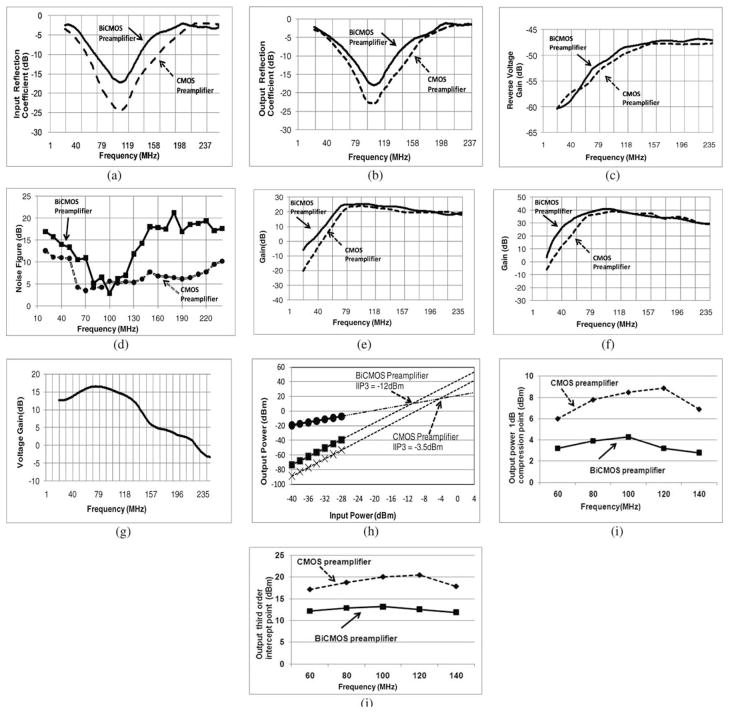
Fig. 10 shows the measured performances of the BiCMOS and CMOS preamplifier, and its front-end circuit and the data are summarized in Table III.
Fig. 10.
Measured performances of an integrated preamplifier and its front-end circuits. (a) Lowest input reflection coefficient: −17.42 dB at 103 M Hz for BiCMOS preamplifier and −27.63 dB at 93 M Hz for CMOS preamplifier. (b) Lowest output reflection coefficient: −21.94 dB at 95 M Hz for BiCMOS preamplifier and −22.18 dB at 102 M Hz for CMOS preamplifier. (c) Reverse voltage gain: −50.67 dB at 80 M Hz for BiCMOS preamplifier and −51.97 dB at 80 M Hz for CMOS preamplifier. (d) Lowest noise figure: 2.9 dB at 100 M Hz for BiCMOS preamplifier and 3.51 dB at 70 M Hz for CMOS preamplifier. (e) Voltage gain of integrated preamplifier: for BiCMOS preamplifier, peak voltage gain is 25.8 dB at 100 M Hz, −3-dB bandwidth is 82%, and −6-dB bandwidth is 130%. For CMOS preamplifier, peak voltage gain is 24.08 dB at 93 M Hz, −3-dB bandwidth is 79%, and −6-dB bandwidth is 183%. (f) Voltage gain of front-end circuits: for BiCMOS preamplifier and filter, voltage gain is 41.28 dB at 100 M Hz, −3-dB bandwidth is 33%, and −6-dB bandwidth is 91%. For CMOS preamplifier and filter, voltage gain is 39.52 dB at 99 M Hz, −3-dB bandwidth is 58%, and −6-dB bandwidth is 108%. (g) Voltage gain graph of Sallen-Key active Butterworth filter: 16.35 dB at 80 M Hz. (h) IIP3 of an integrated preamplifier: IIP3 of BiCMOS preamplifier is −12 dBm and IIP3 of CMOS preamplifier is −3.5 dBm. (i) Output power at 1 dB compression point (OP1dB) versus frequency. (j) Output third-order intercept point (OIP3) versus frequency.
TABLE III.
Comparison Data of BiCMOS and CMOS Preamplifiers.
| Preamplifier | Input reflection coefficient | Reverse gain | Voltage gain | Output reflection coefficient | Noise figure |
|---|---|---|---|---|---|
| BiCMOS | −17.42 | −50.67 | 25.8 | −21.94 | 2.9 |
| CMOS | −27.63 | −51.97 | 24.08 | −22.18 | 3.51 |
The measured input reflection coefficient and output reflection coefficient values show that the lowest point deviates slightly from 100 M Hz, although they demonstrate desirable performances which should be less than −10 dB at 100 M Hz. The measured noise figure of CMOS preamplifier shows that it drops rapidly from 50 M Hz. Therefore, the simulated lowest noise figure of the CMOS preamplifier is 6.5 dB at 100 M Hz, but the measured noise figure at 100 M Hz is 5.61 dB and the measured lowest noise figure is 3.51 dB at 70 M Hz. The difference between simulated data and measured data may come from the off-chip components such as inductors and capacitors, because the simulation model of the parasitic impedances for the off-chip components from the manufacturers is not sufficient to obtain accurate data. The reverse gain is approximately −50 dB around 80 M Hz, which represents good isolation from output port to input port. From Fig. 10(f), the measured voltage gain is the summed result of Figs. 10(e) and 10(f) and the buffer. We place the buffer in the last stage to compensate for the degraded performances of the active filter in the higher frequency range (>120 M Hz) because a high voltage gain (about 15 dB) and impedance mismatch in the active filter would degrade the performance of the front-end circuit in the high-frequency range.
From Fig. 10(h), the dot-dashed lines with circles stand for the fundamental output power of the BiCMOS and CMOS preamplifier. The dashed lines with squares and dashed lines with crosses stand for the third-order intermodulation product of BiCMOS and CMOS preamplifier. The output power at 1 dB compression point (OP1dB) versus frequency and output third-order intercept point (OIP3) are shown in Figs. 10(i) and 10(k). The OIP3 of the BiCMOS preamplifier is around 11 or 12 dBm and that of the CMOS preamplifier is between 17 and 21 dBm, between 60 and 140 M Hz. The OP1dB of the BiCMOS preamplifier is between 2 and 5 dBm and that of the CMOS preamplifier is between 6 and 9 dBm, between 60 and 140 M Hz. The high gain and limited supply voltage cause the integrated preamplifiers to have a relatively low linearity performance; however, the performance can be improved by modifying the preceding stages, such as filter and buffer [18].
The voltage gain of the front-end circuits could be variable to avoid clamping of the signal. The maximum voltage gain of the BiCMOS and CMOS preamplifier is around 24 dB. Therefore, the maximum echo signal should be around 114 mV limited by the supply voltage. The echo signals in the experiment were so low (<50 mV) that the clamping of the signal was avoided. If the echo signal is more than 114 mV, the voltage gain of the preamplifier should be variable. This means that the resonant-load tank circuits for each cascade amplifier must use variable resistors to control the voltage gain. Otherwise, the voltage gain of the active Sallen-Key filter must be made variable or the voltage gain of the power amplifier which triggers the transducer must be adjustable.
C. Pulse-Echo Responses of a Ultrasonic Transducer With Front-End Circuits
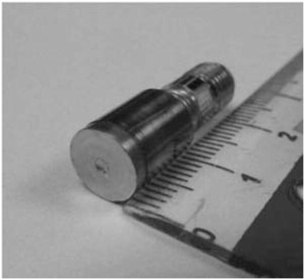
A pulse-echo response measurement is commonly made to evaluate the performance of an ultrasonic transducer and associated electronics [19]. The LiNbO3 transducer (Fig. 11) was tested in a water tank with quartz as a reflector. A monocycle generator (AVTECH AVB2-THE-C, Avtech Electrosystems Ltd., Ottawa, Ontario, Canada), expander, limiter, and designed front-end circuits were used in the measurement, and the echo signal from the transducer was recorded with an oscilloscope (LeCroy 9350AL, LeCroy Corp., Chestnut Ridge, NY). Input and output 50-Ω coaxial cables (Pomona 2249-C-60, Pomona Electronics Inc., Everett, WA) were used. Table IV shows the parameters of an ultrasonic transducer.
Fig. 11.
Photo of high-frequency transducer.
TABLE IV.
The Parameters of a Single-Element 100-MHz Ultrasonic Transducer.
| Center frequency | −6-dB bandwidth | Focus | Aperture size |
|---|---|---|---|
| 79.21 MHz | 50.35% | 2.28 mm | 1.3 mm |
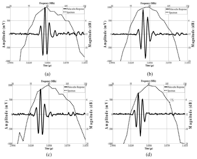
The echo data of the transducer (Fig. 11) showing the center frequency, −6-dB bandwidth, and received peak-to-peak voltage are shown in Fig. 12.
Fig. 12.
(a) LiNbO3 focused transducer’s pulse-echo response using Panametrics 5900PR (gain = 40 dB): center frequency is 82.91 M Hz, −6-dB bandwidth is 51.58%, and received peak-peak voltage is 1769 mV. (b) LiNbO3 focused transducer’s pulse-echo response using BiCMOS preamplifier with Sallen-Key filter: center frequency is 78.23 M Hz, −6-dB bandwidth is 51.70%, and received peak-peak voltage is 1812 mV. (c) LiNbO3 focused transducer’s pulse-echo response using Panametrics 5900PR (gain = 38 dB): center frequency is 82.76 M Hz, −6-dB bandwidth is 53.73%, and received peak-peak voltage is 154 6mV. (d) LiNbO3 focused transducer’s pulse-echo response using CMOS preamplifier with Sallen-Key filter: center frequency is 83.54 MHz, −6-dB bandwidth is 52.33%, and received peak-peak voltage is 1468 mV.
Because the integrated preamplifier has negative voltage gain, the pulse-echo data show an inverted waveform. Pulse-echo responses including the front-end circuits exhibit comparable performances to a Panametrics 5900PR (Olympus NDT Inc., Waltham, MA), with lower ring down and smoother spectrum shape.
D. Wire Phantom Images of an Ultrasonic Transducer With Front-End Circuits
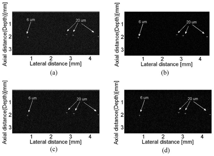
The wire phantom consisted of 4 tungsten wires: one 6-μm-diameter and three 20-μm-diameter. All wire phantom images (Fig. 13) were acquired with an ultrasound biomicroscope (UBM) system developed in-house and are displayed in a 50 dB dynamic range. The mechanic motor was controlled by servo motor controller in Labview (National Instruments, Austin, TX) to scan a cross-section of the wires. The generated RF signals were received by a 12-bit data acquisition board (Gage Applied Technologies, Lockport, IL) and the wire phantom images were post-processed in Labview.
Fig. 13.
Wire phantom images: (a) a transducer and Panametrics 5900PR with 40 dB gain, (b) a transducer and designed front-end system based on BiCMOS preamplifier, (c) a transducer and Panametrics 5900PR with 38 dB gain, and (d) a transducer and designed front-end system based on CMOS preamplifier.
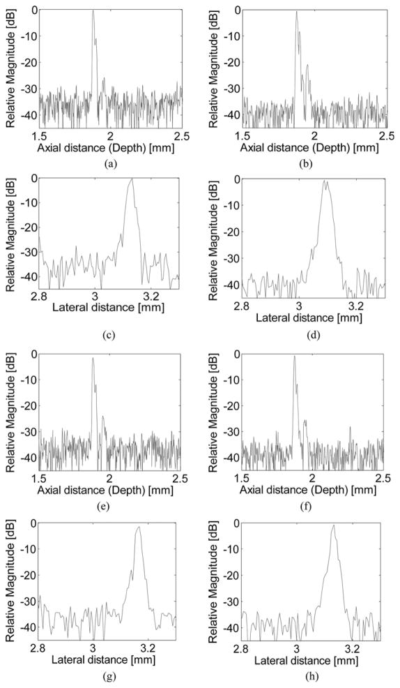
The images show a comparison of the axial and lateral resolution between a Panametrics 5900PR and the frontend system. The axial and lateral resolution of the frontend circuits based on the BiCMOS and CMOS preamplifier show better SNR than the Panamterics 5900PR in Fig. 14; the data are summarized in Table V. The −6-dB axial and lateral resolution of the front-end circuits based on the BiCMOS preamplifier are 14 and 30 μm in Figs. 14(b) and 14(d). The −6-dB axial and lateral resolution of the front-end circuits based on the CMOS preamplifier are 13 and 21 μm in Figs. 14(f) and 14(h). The −6-dB axial and lateral resolution of the Panametrics 5900PR with 40 and 38 dB gain are 14 and 23 μm in Figs. 14(a), 14(c), 14(e), and 14(g). Therefore, the axial and lateral resolutions of the front-end circuits based on the both CMOS and BiCMOS preamplifier are compatible to those obtained with Panametrics 5900PR.
Fig. 14.
(a) Axial resolution of Panametric 5900PR with 40 dB gain. (b) Axial resolution of designed front-end system based on the front-end circuits based on BiCMOS preamplifier. (c) Lateral resolution of Panametric 5900PR with 40 dB gain. (d) Lateral resolution of designed front-end circuits based on the BiCMOS preamplifier. (e) Axial resolution of Panametric 5900PR with 38 dB gain. (f) Axial resolution of designed front-end circuits based on the CMOS preamplifier. (g) Lateral resolution of Panametric 5900PR with 38 dB gain. (h) Lateral resolution of designed front-end circuits based on the CMOS preamplifier.
TABLE V.
Comparison Data of −6-dB Axial and Lateral Resolution.
| Panametrics 5900PR with 40 dB gain | Front-end circuits based on the BiCMOS preamplifier | Panametrics 5900PR with 38 dB gain | Front-end circuits based on the CMOS preamplifier | |
|---|---|---|---|---|
| −6-dB axial resolution (μm) | 14 | 14 | 14 | 13 |
| −6-dB lateral resolution (μm) | 23 | 30 | 23 | 21 |
The integrated preamplifiers are shown to yield lower noise figure and dc power consumption at higher frequencies than devices reported in the literature. However, in these devices, off-chip inductors and capacitors would be needed to optimize their performances. Table VI gives a comparison of the integrated preamplifiers for ultrasonic transducer applications published in the literature and this design.
TABLE VI.
Comparison Data With Other Preamplifiers for Ultrasonic Transducer.
| Paper | Process | Gain (dB) | Bandwidth | Frequency (MHz) | Power (mW) | NF or Input-referred noise | Target application |
|---|---|---|---|---|---|---|---|
| [20] | CMOS | 100 | 990 Hz | 3.5 | 3.4 | — | Transducer |
| [21] | CMOS | 22 | 6.5 MHz | 10 | — | 9.4 nV/√Hz | CMUT |
| [22] | CMOS | 12 | 32 MHz | 20 | 20 | 6.3 nV/√Hz | Ultrasound probe |
| [23] | CMOS | 23 | 1.5 MHz | 2 | 2 | 6.45 nV/√Hz | CMUT |
| [24] | CMOS | — | — | 3 | 0.12 | — | CMUT |
| [5] | CMOS | 14 | 7 MHz | 3 | 600 to 1050 | — | RT3DU transducer |
| [25] | CMOS | 18.9 | 15 to 45 MHz | 30 | 0.598 | — | CMUT |
| [26] | DMOS | 40 | 25 MHz | — | 150 | — | CMUT |
| [27] | CMOS | 40 | 10 MHz | — | 4 | — | CMUT |
| [28] | CMOS | 5 to 20 | >75 MHz | — | — | 10 dB | Piezoelectric MEMS transducer |
| This | BiCMOS | 25.8 24.08 |
82 MHz 73 MHz |
100 93 |
49.53 43.57 |
2.9 dB 5.61 dB |
Piezoelectric transducer |
For CMUT applications or commercial ultrasound analog front-end circuits, the operational-amplifier-based preamplifier without impedance matching circuits is used. The designed preamplifier uses fewer transistors and lower values of resistances than an operational-amplifier-based preamplifier, thus generating lower noise figure (2.9 dB) and smaller power consumption (49.53 mW) than an operational-amplifier-based preamplifier (150 mW power consumption from Wygant et al. [26], 10 dB noise figure from Kim et al. [28]). It also has more freedom in choosing the resonance center frequency because the center frequency can also be determined by off-chip inductors and capacitors rather than by the transistors and feedback loop resistors in the operational-amplifier-based topology. The designed preamplifier must use inductors and capacitors for matching electrical impedance and improved voltage gain, causing the size of the chip to be larger than an operational-amplifier-based preamplifier if the operating frequency of the preamplifier is relatively low. Therefore, this designed preamplifier could be more desirable if the operating frequency of the devices is a few hundred megahertz to allow integration without the external inductors so that the inductance values of the resonant-load tank and impedance matching circuits can be lower, thus reducing the spaces in the chip. If the operating frequency of the transducer is low, active inductor design using transistors is also an alternative way to replace the off-chip passive inductor [29], [30]. The drawback is that the active inductor may degrade the noise performance of the preamplifier, while reducing the chip space.
IV. Conclusion
This paper reports the design and measured performances of an integrated preamplifier and filter chain with a single-element ultrasonic transducer. In these integrated preamplifiers, impedance matching with a high-frequency ultrasonic transducer, voltage gain, center frequency, −6-dB bandwidth, and noise figure can be more easily controlled than in operational amplifiers. The measured peak voltage gain of the BiCMOS preamplifier with the filter was 41.28 dB at 100 M Hz, the −6-dB bandwidth was 91%, and dc power consumption of the BiCMOS preamplifier was 49.53 mW. The peak voltage gain of the CMOS preamplifier with the filter was 39.52 dB at 100 M Hz, the −6-dB bandwidth was 108%, and dc power consumption of the CMOS preamplifier was 43.57 mW. These experimental results show good performance of the integrated preamplifier compared with a Panametrics 5900PR and other preamplifiers for high-frequency transducers. This effort represents the first step in the eventual realization of a complete integrated high-frequency receiving system.
Acknowledgments
The authors acknowledge NIH Grant #P41-EB2182 and MOSIS MEP Research Program #4793-MEP-RES/USC-BE.
Biographies
Hojong Choi received the B.E. degree in electronics and telecommunication engineering from Kyunghee Univeristy, Yongin, Korea, in 2000, and the M.S. in electrical engineering from University of Southern California, Los Angeles, CA, in 2004. He is currently a Ph.D. candidate in the Electrical Engineering Department of the University of Southern California. His current research interests include the integrated circuit design of analog front-end pre-amplifiers, power amplifiers, high-voltage multiplexers, and power protection devices for high-frequency ultrasonic transducers and ultrasound imaging systems.

Xiang Li received a B.E. degree from Zhejiang University, China, in 2007, and a B.S. degree from University of Southern California (USC), Los Angeles, CA, in 2010. He is currently a Ph.D. candidate in the Department of Biomedical Engineering at USC. He started his Ph.D. study in 2008 under the support of the USC Provost’s Fellowship. In 2010, he won the Student Paper Competition Award at the IEEE International Ultrasonics Symposium, San Diego, CA. Under the direction of Dr. Qifa Zhou and Dr. K. Kirk Shung, Xiang is conducting his research in the NIH Ultrasonic Transducer Resource Center (UTRC ) on high-frequency ultrasonic transducer technology, integrated IVUS-OCT imaging, and intravascular photoacoustic imaging.

Sien-Ting Lau received the B.Sc. with 1st Class Honors, M.Phil. and Ph.D. degrees in 1998, 2001, and 2004, respectively, all from the Hong Kong Polytechnic University. From 2004 to 2009, she was with the Department of Applied Physics at the Hong Kong Polytechnic University, first as a Postdoctoral Fellow, then as a Research Associate working on ferroelectric materials characterizations and ultrasonic transducer and array fabrication.
Currently, she is a Research Associate at the NIH Resource Center for Medical Ultrasonic Transducer Technology and the Department of Biomedical Engineering at the University of Southern California, Los Angeles, CA.
Her main research interests are in the development of ferroelectric polymers and composites, MEMs technology, and design and fabrication of high-frequency ultrasonic transducers for medical applications. She has published more than 50 international journal publications with a number of papers published in journals including Applied Physics Letters, the Journal of Applied Physics, and Advanced Materials.

Changhong Hu received his B.S. degree in biomedical engineering from Xi’an Jiaotong University in 1995, Xi’an, Shannxi, P.R China; his M.S. degree in bioengineering from The Pennsylvania State University, University Park, PA, in 2002; and his Ph.D degree in biomedical engineering from the University of Southern California, Los Angeles, CA, in 2005. He worked as a Research Associate and Research Assistant Professor in the Biomedical Engineering Department, University of Southern California, from 2006 to 2010, where he was working on the development of high-frequency ultrasound imaging systems/electronics and digital signal processing. He is currently working at Philips Inc.

Qifa Zhou received his Ph.D. degree from the Department of Electronic Materials and Engineering at Xi’an Jiaotong University, China in 1993. He is currently a Research Professor at the NIH Resource on Medical Ultrasonic Transducer Technology and the Department of Biomedical Engineering at the University of Southern California (USC), Los Angeles, CA. Before joining USC in 2002, he worked in the Department of Physics at Zhongshan University of China, the Department of Applied Physics at Hong Kong Polytechnic University, and the Materials Research Laboratory at The Pennsylvania State University.
Dr. Zhou is a senior member of IEEE (UFFC Society) and a member of the UFFC Society’s Ferroelectric Committee. He is also a member of the Technical Program Committee of the IEEE International Ultrasonics Symposium. He is an Associate Editor of the IEEE Transactions on Ultrasonics, Ferroelectrics, and Frequency Control. His current research interests include the development of ferroelectric thin films, MEMS technology, nano-composites, modeling and fabrication of high-frequency ultrasound transducers and arrays for medical imaging applications, and photoacoustic imaging. He has published more than 100 papers in these areas.

K. Kirk Shung obtained a Ph.D. degree in electrical engineering from the University of Washington, Seattle, WA, in 1975. He did post-doctoral research at Providence Medical Center in Seattle, WA, for one year before being appointed a research bioengineer holding a joint appointment at the Institute of Applied Physiology and Medicine. He became an assistant professor at the Bioengineering Program, The Pennsylvania State University, University Park, PA in 1979. He was a Distinguished Professor of Bioengineering at Penn State until 2002, when he joined the Department of Biomedical Engineering, University of Southern California, Los Angeles, CA, as a professor. He has been the director of NIH Resource on Medical Ultrasonic Transducer Technology since 1997.
Dr. Shung is a life fellow of IEEE and a fellow of Acoustical Society of America and the American Institute of Ultrasound in Medicine. He is a founding fellow of American Institute of Medical and Biological Engineering. He has served for two terms as a member of the NIH Diagnostic Radiology Study Section. He received the IEEE Engineering in Medicine and Biology Society Early Career Award in 1985 and coauthored a paper that won the best paper award for IEEE Transactions on Ultrasonics, Ferroelectrics and Frequency Control in 2000. He was elected an outstanding alumnus of Cheng-Kung University in Taiwan in 2001. He was selected as the distinguished lecturer for the IEEE UFFC society for 2002–2003. In 2010, he received the Holmes Pioneer Award in Basic Science from American Institute of Ultrasound in Medicine. He is the recipient of the IEEE EMBS academic career achievement award in 2011.
Dr. Shung has published more than 400 papers and book chapters. He is the author of the textbook Principles of Medical Imaging, published by Academic Press in 1992 and the textbook Diagnostic Ultrasound: Imaging and Blood Flow Measurements, published by CRC Press in 2005. He co-edited the book Ultrasonic Scattering by Biological Tissues, published by CRC Press in 1993. Dr. Shung’s research interest is in ultrasonic transducers, high-frequency ultrasonic imaging, ultrasound microbeams, and ultrasonic scattering in tissues.
References
- 1.Shung KK. Diagnostic Ultrasound: Imaging and Blood Flow Measurements. London, UK: Taylor and Francis; 2005. [Google Scholar]
- 2.Hu C-H, Snook KA, Cao PJ, Shung KK. High-frequency ultrasound annular array imaging. Part II: Digital beamformer design and imaging. IEEE Trans Ultrason Ferroelectr Freq Control. 2006 Feb;53(2):309–316. doi: 10.1109/tuffc.2006.1593369. [DOI] [PubMed] [Google Scholar]
- 3.Nondestructive Testing Resource Center. Electrical impedance matching and termination, [Online] Available: http://www.ndt-ed.org/EducationResources/CommunityCollege/Ultrasonics/EquipmentTrans/impedancematching.htm.
- 4.Lee TH. The Design of CMOS Radio-Frequency Integrated Circuits. 2. New York, NY: Cambridge University Press; 2004. [Google Scholar]
- 5.Morizio J, Guhados S, Castellucci J, von Ramm O. 64-channel ultrasound transducer amplifier. IEEE Southwest Symp Mixed-Signal Design. 2003:228–232. [Google Scholar]
- 6.Floyd BA, Ozis D. Low-noise amplifier comparison at 2 GHz in 0.25-μm and 0.18-μm and SiGe BiCMOS. IEEE Radio Frequency Integrated Circuits Symp. 2004:185–188. [Google Scholar]
- 7.IBM Microelectronics Division. Introduction to IBM SiGe technologies. East Fishkill; NY: Sep, 2001. pp. 1–15. [Google Scholar]
- 8.Pawlikiewicz AH, Hess D. RF CMOS or SiGe BiCMOS in RF mixed signal circuit design. Proc IEEE Mixed Design of Integrated Circuits and Systems. 2007 Aug;:333–338. [Google Scholar]
- 9.IBM Microelectronics Division. Analog and mixed signal application note varactor devices. East Fishkill; NY: Dec, 2002. pp. 1–6. [Google Scholar]
- 10.Razavi B. Design of Analog CMOS Integrated Circuits. New York, NY: McGraw-Hill; 2000. pp. 224–228. [Google Scholar]
- 11.Razavi B. RF Microelectronics. Upper Saddle River, NJ: Pearson Education; 2003. pp. 171–175. [Google Scholar]
- 12.Ardizzoni J. Universal evaluation board for high speed op amps in SOT-23-5/S packages. AN-674. Analog Devices; Norwood, MA: 2008. [Google Scholar]
- 13.Gray P, Hurst P, Lewis S, Meyer R. Analysis and Design of Analog Integrated Circuits. 4. New York, NY: Wiley; 2001. [Google Scholar]
- 14.Hasting A. Art of Analog Layout. 2. Upper Saddle River, NJ: Prentice Hall; 2005. [Google Scholar]
- 15.IBM Microelectronics Division. Analog and mixed signal application note ESD protection SiGeHP, SiGe5AM, BiCMOS 5DM, and BiCMOS 6HP technologies. East Fishkill; NY: Nov, 2002. pp. 7–9. [Google Scholar]
- 16.Three methods of noise figure measurement. Sunnyvale, CA: Nov 21, 2003. Application Note 2875. [Google Scholar]
- 17.A gilent Technologies Inc. Application Note 57–1. Santa Clara, CA: Aug 5, 2010. Fundamentals of RF and microwave noise figure measurements. [Google Scholar]
- 18.Razavi B. RF Microelectronics. Upper Saddle River, NJ: Pearson Education; 2003. pp. 24–25. [Google Scholar]
- 19.Zhao J-Z, Alves CHF, Snook KA, Cannata KM, Chen W-H, Meyer RJ, Jr, Ayyappan S, Ritter TA, Shung KK. Performance of 50MHz transducers incorporating fiber composite, PVDF, PbTiO3 and LiNbO3. IEEE Ultrasonics Symp. 1999:1185–1190. [Google Scholar]
- 20.Chebli R, Kassem A, Sawan M. Logarithmic programmable preamplifier dedicated to ultrasonic receivers. IEEE Circuits and Systems Symp. 2002:673–676. [Google Scholar]
- 21.Noble RA, Davies RR, King DO, Day MM, Jones ARD, Intosh JSM, Hutchins DA, Saul P. Low-temperature micromachined cMUTs with fully-integrated analogue front-end electronics. IEEE Ultrasonics Symp. 2003:1045–1050. [Google Scholar]
- 22.Lay LL, Carey SJ, Hatfield JV. Pre-amplifier arrays for intra-oral ultrasound probe receiving electronics. IEEE Ultrasonics Symp. 2005:1753–1756. [Google Scholar]
- 23.Cicek I, Bozkurt A, Karaman M. Design of a front-end integrated circuits for 3D acoustic imaging using 2-D CMUT arrays. IEEE Trans Ultrason Ferroelectr Freq Control. 2005 Dec;52(12):2235–2241. doi: 10.1109/tuffc.2005.1563266. [DOI] [PubMed] [Google Scholar]
- 24.Peng S-Y, Qureshi MS, Basu A, Guldiken RO, Degertekin FL, Hasler PE. Floating-gate based CMUT sensing circuit using capacitive feedback charge amplifier. IEEE Ultrasonics Symp. 2006:2425–2428. [Google Scholar]
- 25.Cenkeramaddi LR, Singh T, Ytterdal T. Inverter-based 1V transimpedance amplifier in 90nm CMOS for medical ultrasound imaging. Norchip Conf. 2009:1–4. [Google Scholar]
- 26.Wygant IO, Jamal NS, Lee HJ, Nikoozadeh A, Oralkan O, Karaman M, Khuri-Yakub BT. An integrated circuit with transmit beamforming flip-chip bonded to a 2-D CMUT array for 3-D ultrasound imaging. IEEE Trans Ultrason Ferroelectr Freq Control. 2009 Oct;56(10):2145–2156. doi: 10.1109/TUFFC.2009.1297. [DOI] [PubMed] [Google Scholar]
- 27.Wygant IO, Zhuang X, Yeh DT, Oralkan O, Ergun AS, Karaman M, Khuri-Yakub BT. Integration of 2D CMUT arrays with front-end electronics for volumetric ultrasound imaging. IEEE Trans Ultrason Ferroelectr Freq Control. 2008 Feb;55(2):327–342. doi: 10.1109/TUFFC.2008.652. [DOI] [PubMed] [Google Scholar]
- 28.Kim I, Kim H, Griggio F, Tutwiler RL, Jackson TN, Trolier-McKinstry S, Choi K. CMOS ultrasound transceiver chip for high-resolution ultrasonic imaging systems. IEEE Trans Biomed Circuits Syst. 2009 Oct;3(5):293–303. doi: 10.1109/TBCAS.2009.2023912. [DOI] [PubMed] [Google Scholar]
- 29.Leifso C, Haslett JW. A fully integrated active inductor with independent voltage tunable inductance and series-loss resistance. IEEE Trans Microw Theory Tech. 2001 Apr;49(4):671–676. [Google Scholar]
- 30.Yang K-N, Cheng Y-C, Hsu T-Y, Hsu T-R, Lee C-Y. A 1.75GHz inductor-less CMOS low noise amplifier with high-Q active inductor load. Proc IEEE Midwest Symp Circuits and Systems. 2001 Aug;:816–819. [Google Scholar]


