Abstract
The commonly used optical sensor based on surface plasmon-polariton wave phenomenon can sense just one chemical, because only one SPP wave can be guided by the interface of a metal and a dielectric material contained in the sensor. Multiple analytes could be detected and/or the sensing reliability for a single analyte could be enhanced, if multiple SPP-wave modes could be excited on a single metal/dielectric interface. For that to happen, the partnering dielectric material must be periodically non-homogeneous. Using a chiral sculptured thin film (CSTF) as that material in a SPP-wave platform, we show that the angular locations of multiple SPP-wave modes shift when the void regions of the CSTF are infiltrated with a fluid. The sensitivities realized in the proof-of-concept experiments are comparable to state-of-research values.
Straddling the boundary of two materials, a surface wave is a delicate phenomenon. Any alteration in the constitution of either of the two partnering materials will alter the characteristics of the surface wave, which makes this phenomenon highly suitable for sensing applications. An electromagnetic surface wave commonly used for optical sensing of chemical and biochemical analytes1,2,3 in a host of research settings spanning chemistry, physics, life sciences, engineering, food science, agriculture, forensic science, pharmaceuticals, and pathology is the surface-plasmon-polariton (SPP) wave. The propagation of an SPP wave is guided by the interface of a metal and a dielectric material4,5. Microscopically, the SPP wave results from the interaction of free electrons in the metal and polaritons in the dielectric material to form quasiparticles called plasmon-polaritons that propagate along the interface.
Optical techniques requiring just a prism of high refractive index, as demonstrated by Otto6 and Kretschmann and Raether7, made the excitation of SPP waves so inexpensive that SPP-wave-based optical sensors became commonplace by the early 1990s. In one commonly used configuration, a metal thin film with a thickness on the order of a few tens of nanometers is deposited onto the hypotenuse of a 45°-90°-45° prism, and air is the partnering dielectric material. When monochromatic light is incident on one of the slanted faces of the prism such that the magnetic field of light is directed tangentially to that face (i.e., the light is p polarized), and the angle of incidence on the prism/metal interface θ is such that no transmission of optical energy occurs across the metal (because θ exceeds the critical angle for a fictitious prism/air interface), most of the light is reflected through the other slanted face of the prism. The balance is absorbed. When the absorptance is plotted against θ, a peak indicates the excitation of an SPP wave guided by the metal/air interface.
Suppose that air is replaced by a fluid such as water. Then, the p-polarized plane wave has to arrive at a higher angle of incidence in order to excite the SPP wave10. The increase in the value of θ is the basis of numerous commercially available SPP-wave-based sensors8 capable of label-free and real-time detection of a huge variety of analytes1,2.
The chief disadvantage of these commercially available SPP-wave-based sensors is that they are limited to detecting one analyte at a time, since only one SPP wave of a specific frequency can be guided by a metal/dielectric interface. Spatial arrays of multiple sensors are needed to detect multiple analytes simultaneously. If multiple SPP-wave modes could be guided at a specified frequency by a metal/dielectric interface, multiple channels per sensor will become available to sense multiple analytes. Alternatively, the sensing of one analyte could be done reliably through those multiple channels. Both of these possibilities motivated the work presented here.
During the last five years, theory has demonstrated that multiple SPP-wave modes can indeed be guided by the interface of a metal and a dielectric material, provided that the dielectric material is periodically non-homogeneous normal to the interface9,10,11. Characteristics such as phase speed, attenuation rate, and spatial profiles of the electromagnetic fields are different from one SPP-wave mode to another, but all have the same frequency. Furthermore, the excitation of multiple SPP-wave modes along the interface of a metal and a periodically non-homogeneous dielectric material at a single frequency has been experimentally demonstrated12,13,14,15.
In Refs 9,10,11,12,13,14,15, the periodically non-homogeneous dielectric material is either an isotropic rugate filter11 or a sculptured thin film (STF) that is periodically non-homogeneous along its thickness direction9,10,12,13,14,15. STFs are a class of nano-engineered, unidirectionally non-homogeneous, and anisotropic thin films that can be fabricated using a variety of physical vapor deposition (PVD) techniques16,17. Typically, a collimated vapor flux is directed toward a substrate which is rocking and/or rotating in a low-pressure vacuum chamber17. One type of STF is a sculptured nematic thin film (SNTF) that is fabricated by rocking the substrate about an axis that is tangential to the substrate plane. Another type of STF is a chiral STF (CSTF) which is fabricated when the substrate is rotated at a constant rate about an axis which passes normally through it. Both metal/SNTF13 and metal/CSTF interfaces12,14,15 have been experimentally shown to support the propagation of multiple SPP-wave modes at a single frequency.
Any STF is porous, with porosity ranging from 10% to 90%, depending on the material evaporated and the substrate dynamics17,18. When the porous regions of an STF are infiltrated with a fluid, its optical characteristics change19,20. Theory has shown21 that when a periodically non-homogeneous STF would be incorporated in an SPP-wave-based sensor, multiple SPP-wave modes allowed at a single frequency would enhance sensing capabilities significantly.
In this communication, we report experimental evidence of this theoretical result. We show that a multiple SPP-wave platform exemplified by a metal/CSTF combination in the commonly used prism-coupled configuration supports the propagation of three distinct SPP-wave modes at a single frequency. When infiltrated with water or a sucrose solution, the number of SPP-wave modes reduces to two. The angles of incidence of the absorptance peaks are different on infiltration by the different fluids. As a consequence, our work opens up two research avenues for SPP-wave-based sensors: (i) more reliable sensing of a single analyte, and (ii) simultaneous sensing of multiple analytes.
Results
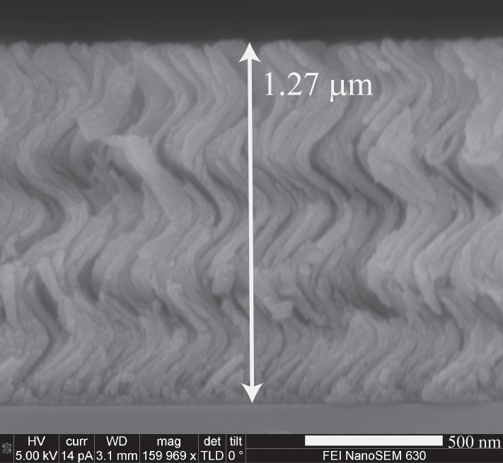
Figure 1 shows the cross-sectional image of an SPP-wave platform incorporating the interface of a thin aluminum film and a lanthanum-fluoride CSTF on a silicon substrate. This substrate was chosen in order to obtain cross-sectional images on a field-emission scanning electron microscope (FE-SEM). The CSTF displays periodic and non-homogenous chiral morphology. The average film thickness is 1.27 μm which is in good agreement with a 1.20-μm-thick film as indicated by an in-situ quartz crystal monitor during thin-film deposition. The CSTF is three periods thick, each period being ~400 nm.
Figure 1. Multiple SPP-wave platform for optical sensing.
High-resolution cross-section FE-SEM image of platform A containing a three-period CSTF made by directing a collimated vapor of LaF3 at an angle χv = 15° to the plane of a substrate rotating at about 0.06 rpm at 6.5 × 10⁻⁶ Torr base pressure. The period of the CSTF is ~400 nm. Underneath is a 30-nm-thick film of Al that had been deposited on a stationary silicon substrate at 1.5 × 10⁻⁵ Torr base pressure and χv = 90°. The silicon substrate was used in order to obtain this image; otherwise, a dense flint glass (SF11) substrate was used for optical sensing experiments in the prism-coupled configuration. Platform B is similar except that the CSTF has four periods, each ~400 nm thick.
Several replicates of this platform (labeled A) along with several replicates of another platform (labeled B) containing a four-period-thick CSTF were deposited on dense flint glass substrates for optical sensing experiments. The period was maintained as ~400 nm. Lanthanum fluoride was chosen because it is insoluble in water and has a bulk refractive index (nLaF3 = 1.601) higher than that of water (nH2O = 1.333) but lower than that of dense flint glass of type SF11 (nSF11 = 1.778) at room temperature and 1 atm pressure22. For the prism-coupled configuration, a dense flint glass prism was affixed to the dense flint glass substrate with an index-matching liquid (niml = 1.785).
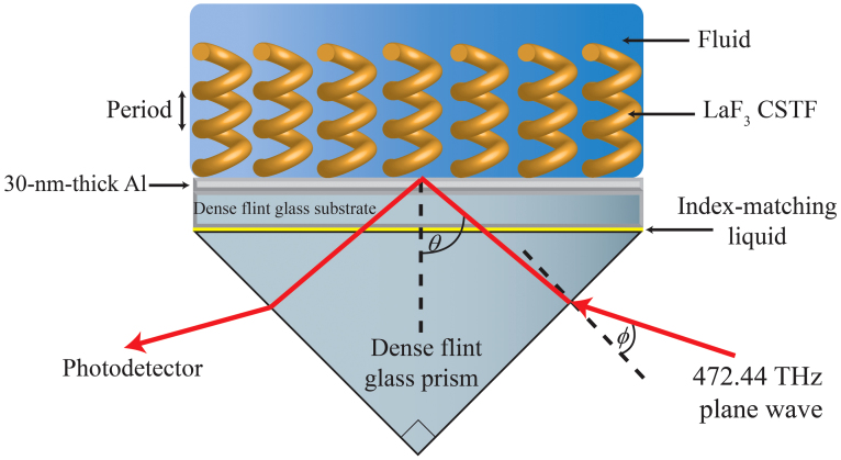
The prism-coupled configuration is shown in Fig. 2 when a fluid infiltrates and lies atop the CSTF. The reflectance of p-polarized light at 472.44 THz was measured using a photodetector as a function of the angle θ = 45° + [sin−1(nSF11−1 sinφ)], where φ is the angle between the direction of the incident light and the normal to the slanted face of the prism on which light is incident. This measurement was made for uninfiltrated platforms as well as for platforms in which the CSTF was infiltrated with deionized water (nH2O = 1.333), 0.183 M aqueous solution of sucrose (n0.183 = 1.340)23, and a 0.367 M aqueous solution of sucrose (n0.367 = 1.351)23. After checking that transmission of optical energy into air beyond the CSTF does not occur in the range of θ investigated, the absorptance can be obtained by subtracting the reflectance from unity. An absorptance peak is then manifested as a reflectance dip.
Figure 2. Schematic of prism-coupled configuration.
The CSTF/metal/substrate platform is affixed to a prism made of the same material as the substrate with an index-matching liquid. Light incident on one slanted face at angle φ is incident on the prism/metal interface at angle θ. This figure shows that the fluid containing the analyte completely infiltrates and lies atop the CSTF.
Uninfiltrated platforms
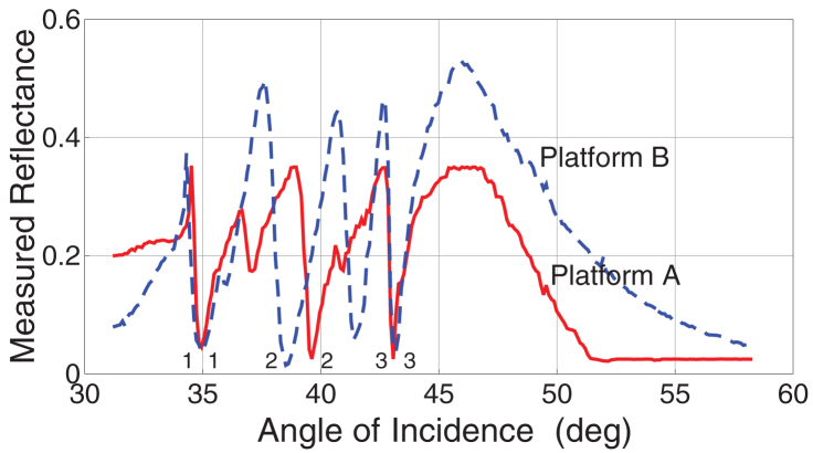
Figure 3 presents typical plots of the reflectance vs. θ for platforms A and B. Pronounced reflectance dips for platform A are located at θ = 34.94°, 37.09°, 39.61°, and 43.06° whereas similar dips for platform B are located at θ = 34.94°, 38.51°, 41.39°, and 43.06°. The angular locations of the leftmost (θ = 34.94°) and the rightmost dips (θ = 43.06°) coincide extremely well, which is a strong indication that both represent two distinct SPP-wave modes11,12,13,14 that are strongly localized to the metal/CSTF interface on the CSTF side. Theoretical understanding13 allows us to conclude that the fields of both SPP-wave modes die out inside the CSTF within a distance of no more than three periods from the metal/CSTF interface. These dips are marked by ‘1' and ‘3' in Fig. 3.
Figure 3. Measured reflectance plots for uninfiltrated platforms.
Reflectance measured as a function of θ at 472.44 THz of platforms A (red solid line) and B (blue dashed line). The incident light is p polarized and the CSTFs are uninfiltrated. The reflectance dips indicating the excitation of an SPP-wave mode are identified by ‘1', ‘2', and ‘3'.
The two reflectance dips labeled ‘2', the one for platform A located at θ = 39.61° and the one for platform B at θ = 38.51°, do not coincide and are 1.1° apart. Either these reflectance dips represent a single SPP-wave mode that is not as strongly localized to the metal/CSTF interface as the ones labeled ‘1' and ‘3', or they represent a waveguide mode25. A waveguide mode would extend over the entire thickness of the partnering dielectric material and its location on the θ axis would change with that thickness25. In contrast, the location of an SPP-wave mode could vary as that thickness increases up to a certain threshold, but not beyond it24.
In order to resolve the nature of the reflectance dips labeled ‘2' in Fig. 3, we computed the propagation constants of different waveguide modes in a homogeneous dielectric slab of refractive index nhds bounded by a perfect electric conductor on one face and air on the other. Since the penetration of electromagnetic fields in a metal cannot occur significantly beyond the skin depth in that metal, and the skin depth for thin-film aluminum is about 30 nm, the replacement of the metal by a perfect conductor simplifies analysis. The refractive index nhds was estimated as the average of nLaF3 and nair = 1.0, with the reasonable assumption that both lanthanum fluoride and air are present in the CSTF in equal volumetric proportions. The propagation constants were divided by the wavenumber in the prism material to obtain the sines of angles that are analogous to θ.
We calculated that waveguide modes should occur at θ ~ 37.1°, 43.6°, and 46.7° in platform A. Evidence of the first waveguide mode (θ ~ 37.1°) is indeed available as a moderate reflectance dip in Fig. 3, but the other two waveguide modes appear to have been excited very weakly, if at all, in the prism-coupled configuration. Waveguide modes could appear at θ ~ 36.5°, 41.9°, 45.2°, and 46.6° in platform B. Evidence of the first waveguide mode (θ ~ 36.5°) is available as a very shallow dip and of the second waveguide mode (θ ~ 41.9°) as a strong dip in Fig. 3, the remaining two waveguide modes being extremely weakly excited if at all. We conclude therefore that the dips marked ‘2' represent a single SPP-wave mode that is localized to the metal/CSTF interface within a distance exceeding at least three periods inside the CSTF24.
Thus, Fig. 3 shows that p-polarized light at 472.44 THz launched three SPP-wave modes in the SPP-wave platform investigated, thereby qualitatively confirming earlier experimental12,14,15 and theoretical10,24 research.
Water-infiltrated platforms
When the air inside and atop the CSTF is replaced by a fluid of a refractive index greater than that of air, theory indicates that a change in the optical properties of the partnering dielectric material seriously affects the SPP-wave phenomenon21. Indeed, the angle of incidence required to excite the (sole) SPP-wave mode is known to increase with increase in the refractive index of the fluid infiltrating a homogeneous, isotropic partnering dielectric material1.
The same trend has been theoretically found for the metal/CSTF interface21. But there is one difference. As the refractive index of the fluid increases towards the refractive index of the skeleton material of the CSTF, the number of SPP-wave modes must tend to unity. This is because the infiltrated CSTF becomes isotropic and homogeneous when the two refractive indexes equal each other26.
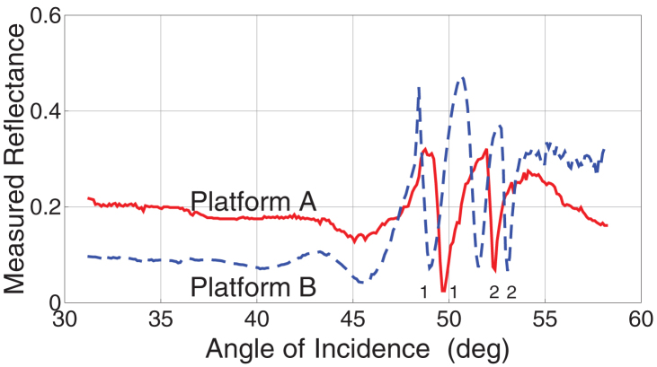
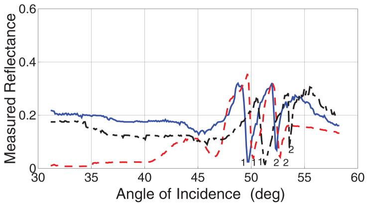
Figure 4 presents typical plots of the reflectance vs. θ for platforms A and B infiltrated by deionized water. Pronounced reflectance dips for platform A are located at θ = 49.65° and 52.17°, and for platform B at θ = 48.98°, 51.52°, and 53.04°. These data indicate a potential reduction in the number of SPP-wave modes as well as shifts to greater angles of incidence to excite those modes.
Figure 4. Measured reflectance plots for water-infiltrated platforms.
Reflectance measured as a function of θ at 472.44 THz of platforms A (red solid line) and B (blue dashed line). The incident light is p polarized and water infiltrates and lies atop the CSTF. The reflectance dips indicating the excitation of an SPP-wave mode are identified by ‘1' and ‘2'.
Although both reflectance dips for platform A are located on the θ axis within a degree of at least one reflectance dip for platform B, the underlying causes for these reflectance dips still need to be ascertained. Therefore, we repeated the analysis for the propagation constants of different waveguide modes in a homogeneous dielectric slab of refractive index nhds bounded by a perfect electric conductor on one face and water on the other. The refractive index nhds was estimated this time as the average of nLaF3 and nH2O, with the assumption that water completely filled the pores of the CSTF. Again, the propagation constants were divided by the wavenumber in the prism material to obtain the sines of angles that are analogous to θ.
Waveguide modes should occur at θ ~ 51.4° and 55.9° in platform A. Neither of these two are easy to find in Fig. 4, indicating that the reflectance dips at θ = 49.65° and 52.17° are indicative of the excitation of two SPP-wave modes.
Waveguide modes should occur at θ ~ 49.4°, 53.3°, and 55.2° in platform B. The leftmost one cannot be seen in Fig. 4, the middle one is strongly present, and the rightmost one has a shallow existence. Accordingly, the strong reflectance dips at θ = 48.98° and 51.52° represent the excitation of two SPP-wave modes. Because their locations on the θ axis are about 0.7° less than those for platform B, we conclude that both of these SPP-wave modes are localized to the metal/CSTF interface within a distance exceeding at least three periods inside the CSTF24. The dips are marked by ‘1' and ‘2' in Fig. 4.
Sucrose-solution-infiltrated platforms
Replicates of the platforms used for the water-infiltration experiments were used for the next two sensing experiments. In the first of these two experiments, a 0.183 M aqueous solution of sucrose (n0.183 = 1.340) infiltrated and lay atop platform A. In the second, a 0.367 M aqueous solution (n0.367 = 1.351) was used instead. The thicker platform B was not used because the viscosity of the solutions could prevent them from reaching the pores close to the interface.
Figure 5 presents typical plots of the reflectance vs. θ for platform A when a sucrose solution infiltrates and lies atop the three-period CSTF. The plot for water-infiltrated platform A is also provided in this figure for comparison. Both SPP-wave modes ‘1' and ‘2' shift to higher values of θ with increase in sucrose content from 0 to 0.367 M (and hence the increase in the refractive index of the infiltrant fluid from 1.333 to 1.351). This figure is the main result of this communication, as it completely validates the theoretical prediction21 of multiple SPP-wave modes available for optical sensing at the interface of a metal and a dielectric material that is a periodically non-homogeneous normal to the interface.
Figure 5. Measured reflectance plots for sucrose-solution-infiltrated platform A.
Reflectance measured as a function of θ at 472.44 THz of platform A when an aqueous solution of sucrose infiltrates and lies atop the three-period CSTF.The incident light is p polarized. The blue solid line is for the 0 M solution, the red dashed line is for the 0.183 M solution, and the black dashed-dotted line is for the 0.367 M solution. The reflectance dips indicating the excitation of the two SPP-wave modes are identified by ‘1' and ‘2'.
Sensitivity
Let θ(ninfil,m) denote the angle of incidence for a reflectance dip indicating the excitation of the SPP-wave mode labeled  in Fig. 5. Then, a sensitivity with respect to water infiltration can be defined as
The sensitivity values for both sucrose solutions and for both SPP-wave modes from Fig. 5 are tabulated in Table 1.
Table 1. Sensitivities ρ(n0.183,m) asnd ρ(n0.367,m) for the mth SPP-wave mode in Figure 5.
| m | ninfil (RIU) | θ(ninfil,m) − θ(nH2O,m) (deg) | ρ (deg/RIU) |
|---|---|---|---|
| 1 | 1.340 | 0.55 | 78.57 |
| 1.351 | 1.54 | 85.55 | |
| 2 | 1.340 | 0.44 | 62.85 |
| 1.351 | 1.68 | 93.33 |
Over the limited range (1.333 to 1.351) of the refractive index of the infiltrant fluid tested, the sensitivity is ~80 deg/RIU. This figure is about three times higher than the one predicted theoretically for a multiple-SPP-wave platform incorporating a titanium-oxide CSTF21. Most likely, the lanthanum-fluoride CSTF used in our experiments is more porous than the titanium-oxide CSTF involved in theoretical prediction.
In the absence of a CSTF, only one SPP-wave mode can propagate guided by a metal/air or a metal/fluid interface at a given frequency. For a single-SPP-wave platform comprising a SF11 prism, a SF11 substrate, and a metal film made of either gold or silver, the dynamic sensitivity
cannot exceed 85 deg/RIU at 472.44 THz27. However, Table 1 yields the ratios
 |
for platform A. Thus, the use of a CSTF has not only delivered multiple SPP-wave modes, each capable of being used for sensing, but also equal or better sensitivity in the prism-coupled configuration27. Further enhancement for commercial purposes would require careful selection of the prism material, the metal, and the CSTF material, as theoretical studies have already shown for single-SPP-wave platforms27. Moreover, the use of a lensing system after the laser-diode module would allow simultaneous measurements for a range of angles θ, and the replacement of the photodetector by an array of charge-coupled device (CCD) sensors would speed up the measurement process28.
Discussion
A multiple SPP-wave-based optical sensor with a single metal/dielectric interface has been demonstrated and confirms previous theoretical predictions, the partnering dielectric material being a chiral sculptured thin film. Improvement in performance will come from optimizing the vapor flux angle during the fabrication of the CSTF. Whereas a CSTF with a high value of χv would have very little porosity and therefore very little sensitivity, a CSTF with a very low value of χv would be so porous as to be fragile. Although only one analyte (i.e., sucrose) was used in the proof-of-concept experiments reported here, the occurrence of multiple SPP-wave modes is exploitable for both more reliable sensing of a single analyte and multi-analyte sensing, using regression analysis29.
More reliable sensing of a simple analyte is possible using Taylor expansions of the shifts θ(ninfil, m) − θ(nH20, m) with respect to ninfil − nH20 for each m, as has been shown for a sensor based on a class of electromagnetic surface waves guided by the interface of two dielectric materials30. The reference infiltrant need not be H2O.
For sensing multiple analytes, layers of different recognition materials will have to be implanted at different depths into the CSTF, care being taken that the implantation depths are such that one of the multiple SPP-wave modes has a maximal electric field at that depth24 in order to perturb the angular location of the reflectance dip significantly. This could be done by short-term co-deposition of a recognition material in addition to one chosen for fabricating the CSTF31. Properly chosen recognition materials would impart specificity of sensing.
Furthermore, as not only p-polarized light but also s-polarized light can excite SPP-wave modes guided by the interface of a metal and a periodically non-homogeneous dielectric material9,10,13, further avenues for multi-analyte sensing are now available for investigation.
In closing, let us mention the imaging SPP-wave sensor in which broadband light is used in place of monochromatic light and the photodetector is replaced by an array of CCD or CMOS sensors. With only one SPP-wave mode launched at a specific frequency, the multi-frequency data is optically manipulated to measure ninfil correct to five decimal digits28. Incorporation of the multiple-SPP-wave platform is expected to enhance the capabilities of imaging SPP-wave sensors as well.
Methods
Deposition of aluminum
A dense flint glass (SF11) substrate (Swiss Jewel Co., Philadelphia, PA, USA) was cleaned in an ultrasonic bath of ethanol for five min and blow-dried with a nitrogen gun before being positioned onto a substrate holder required for thin-film deposition. The substrate holder and the substrate were placed in a low-pressure evaporation chamber in which the resistive-heating PVD technique was employed. At a base pressure of 1.5 × 10⁻⁵ Torr, 35 A current was passed through a tungsten basket housing an aluminum pellet. The aluminum vapor flux was directed towards the substrate until a 30-nm-thick film was produced. The deposition rate monitored using a quartz crystal monitor (Inficon, Bad Ragaz, Switzerland) in situ was kept fixed at 0.4 ± 0.02 nm s−1.
Deposition of CSTF
The low-pressure chamber was opened after the aluminum film had been deposited, was loaded with a notched boat containing LaF3 powder (Phelly Materials, Upper Saddle River, NJ, USA), and then evacuated again. When the base pressure of 6.5 × 10⁻⁶ Torr was reached, a computer-controlled stepper motor tilted the aluminum-coated substrate about an axis tangential to the substrate plane to a fixed angle χv = 15°. Then, a current was passed through the notched boat and increased in increments of 5 A until reaching 95 A in order to generate a LaF3 vapor flux. The deposition rate was kept fixed at 0.4 ± 0.02 nm s−1 while a second computer-controlled stepper motor continuously rotated the substrate holder about an axis which passes normally through it in a clockwise manner when viewed from the vapor source in increments of 18° with a 48-s pause between successive increments. Twenty 18° steps were needed to complete the deposition of one structural period of thickness 2Ω = 400 nm. After the deposition of either three or four periods of the CSTF, the platform was allowed to reach room temperature before the evaporation chamber was exposed to atmosphere. The platform was placed in a low-pressure desiccator for 24 h before its reflectance spectrum was collected.
Optical measurements
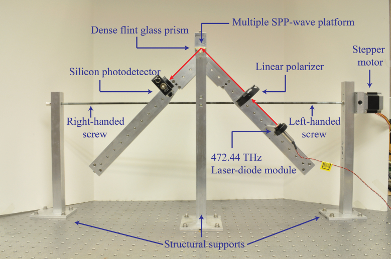
The dense flint glass substrate in the platform was affixed to the hypotenuse of a 45°-90°-45° dense flint glass prism (Edmund Optics, Barrington, NJ, USA) with one drop of an index-matching liquid (Cargille Laboratories, Cedar Grove, NJ, USA). The assembly was then placed onto a custom-built machine shown in Fig. 6. The machine has an incidence arm and reflection arm. A low-power 472.44 THz laser-diode module (ThorLabs, Newton, NJ, USA) followed by a linear polarizer was positioned as the light source on the incidence arm. The intensity of light received by a PDA36A photodetector (ThorLabs, Newton, NJ, USA) on the reflection arm was measured using a TDS 2024B oscilloscope (Tektronix, Beaverton, OR, USA). Dividing the intensity of the reflected light by that of the incident light delivered the reflectance.
Figure 6. Custom-built machine used to perform all experiments with uninfiltrated or infiltrated platforms.
This custom-built machine incorporates a prism-coupled configuration at its apex. As the stepper motor rotates the turnbuckle-style screw, the angle of incidence of the 472.44 THz p-polarized beam on one slanted face of the prism changes and the appropriate voltage readings from an oscilloscope (not shown) connected to the photodetector are recorded.
As the angle between the two arms was changed, the angle φ was increased from −20° to 30° in steps of 0.02°.
For measurements in which the CSTF was infiltrated, a drop of the solution (water, or water containing sucrose) was put on top of the CSTF.
Electron microscopy
An FEI Nova NanoSEM 630 (Hillsboro, OR, USA) field-emission scanning electron microscope was used to image the morphology of the CSTFs.
Author Contributions
S.E.S. and D.P.P. fabricated all thin films and jointly designed and fabricated the custom-built machine which was used for all optical measurements used in this investigation. S.E.S. made all optical measurements. A.L. conducted the waveguide mode analysis and supervised the research. S.E.S. and A.L. were primarily responsible for writing this manuscript.
Acknowledgments
This work was supported in part by the US National Science Foundation under Grant No. CBET-1106503. A.L. and S.E.S. also thank the Charles Godfrey Binder Endowment at the Pennsylvania State University for partial financial support.
References
- Homola J., Yee S. S. & Gauglitz G. Surface plasmon resonance sensors: a review. Sensors & Actuators B: Chemical 54, 3–15 (1999). [Google Scholar]
- Abdulhalim I., Zourob M. & Lakhtakia A. Surface plasmon resonance for biosensing: a mini-review. Electromagnetics 28, 214–242 (2008). [Google Scholar]
- Green R. J., Frazier R. A., Shakesheff K. M., Davies M. C., Roberts C. J. & Tendler S. J. B. Surface plasmon resonance analysis of dynamic biological interactions with biomaterials. Biomaterials 21, 1823–1835 (1999). [DOI] [PubMed] [Google Scholar]
- Maier S. Plasmonics: Fundamentals and Applications (Springer, 2006). [Google Scholar]
- Pitarke J. M., Silkin V. M., Chulkov E. V. & Echenique P. M. Theory of surface plasmon and surface-plasmon polaritons. Reports on Progress in Physics 70, 1–87 (2007). [Google Scholar]
- Otto A. Excitation of nonradiative surface plasma waves in silver by the method of frustrated total reflection. Zeitschrift für Physik 216, 398–410 (1968). [Google Scholar]
- Kretschmann E. & Raether H. Radiative decay of nonradiative surface plasmons excited by light. Zeitschrift für Naturforschung 23a, 2135–2136 (1968). [Google Scholar]
- Schasfoort R. B. M. & Tudos A. J. Handbook of Surface Plasmon Resonance (RSC Publishing, 2006). [Google Scholar]
- Motyka M. A. & Lakhtakia A. Multiple trains of same-color surface plasmon-polaritons guided by the interface of a metal and a sculptured nematic thin film. Journal of Nanophotonics 2, 021910 (2008). [Google Scholar]
- Polo J. A. Jr. & Lakhtakia, A. On the surface plasmon polariton wave at the interface of a metal and a chiral sculptured thin film. Proceedings of the Royal Society of London A 465, 87–107 (2009). [Google Scholar]
- Faryad M. & Lakhtakia A. On surface plasmon-polariton waves guided by the interface of a metal and a rugate filter with a sinusoidal refractive-index profile. Journal of Optical Society of America B 27, 2218–2223 (2010). [Google Scholar]
- Devender, Pulsifer D. P. & Lakhtakia A. Multiple surface plasmon polariton waves. Electronics Letters 45, 1137–1138 (2009). [Google Scholar]
- Lakhtakia A., Jen Y.-J. & Lin C.-F. Multiple trains of same-color surface plasmon-polaritons guided by the interface of a metal and sculptured nematic thin film. Part III: Experimental evidence. Journal of Nanophotonics 3, 033506 (2009). [Google Scholar]
- Gilani T. H., Dushkina N., Freeman W. L., Numan M. Z., Talwar D. N. & Pulsifer D. P. Surface plasmon resonance due to the interface of a metal and a chiral sculptured thin film. Optical Engineering 49, 120503 (2010). [Google Scholar]
- Kim J. B., Zou Y., Kim Y. D., Kim J. J. & Hwangbo C. K. Multiple surface plasmon waves in [prism/Ag/SiO2 helical thin film]. Kretschmann configuration. Thin Solid Films 520, 1451–1453 (2011). [Google Scholar]
- Robbie K., Brett M. J. & Lakhtakia A. Chiral sculptured thin films. Nature 384, 616 (1996). [Google Scholar]
- Lakhtakia A. & Messier R. Sculptured Thin Films: Nanoengineered Morphology and Optics (SPIE Press, 2005). [Google Scholar]
- Robbie K. & Brett M. J. Sculptured thin films and glancing angle deposition: Growth mechanics and applications. Journal of Vacuum Science and Technology A 3, 1460–1465 (1997). [Google Scholar]
- Lakhtakia A., McCall M. W., Sherwin J. A., Wu Q. H. & Hodgkinson I. J. Sculptured-thin-film spectral holes for optical sensing of fluids. Optics Communications 194, 33–46 (2001). [Google Scholar]
- Pursel S. M. & Horn M. W. Prospects for nanowire sculptured-thin-film devices. Journal of Vacuum Science and Technology B 25, 2611–2615 (2007). [Google Scholar]
- Mackay T. G. & Lakhtakia A. Modeling chiral sculptured thin films as platforms for surface-plasmonic-polaritonic optical sensing. IEEE Sensors Journal 12, 273–280 (2012). [Google Scholar]
- Haynes W. M., ed. CRC Handbook of Chemistry and Physics (CRC Press, 2012). [Google Scholar]
- Mehan N., Gupta V., Sreenivas K. & Mansingh A. Surface plasmon resonance based refractive index sensor for liquids. Indian Journal of Pure & Applied Physics 43, 854–858 (2005). [Google Scholar]
- Polo J. A. Jr., Mackay T. G. & Lakhtakia A. Mapping multiple surface-plasmon-polariton-wave modes at the interface of a metal and a chiral sculptured thin film. Journal of Optical Society of America B 28, 2656–2666 (2011). [Google Scholar]
- Kapany N. S. & Burke J. J. Optical Waveguides (Academic Press, 1972). [Google Scholar]
- Lakhtakia A. Enhancement of optical activity of chiral sculptured thin films by suitable infiltration of void regions. Optik 112, 145–148 (2001). [Google Scholar]
- Homola J., Koudela I. & Yee S. Surface plasmon resonance sensors based on diffraction gratings and prism couplers: sensitivity comparison. Sensors and Actuators B: Chemical 54, 16–24 (1999). [Google Scholar]
- Wong C. L. et al. Multiplex spectral surface plasmon resonance imaging (SPRI) sensor based on the polarization control scheme. Optics Express 19, 18965–18978 (2011). [DOI] [PubMed] [Google Scholar]
- Draper N. R. & Smith H. Applied Regression Analysis (Wiley, 1998). [Google Scholar]
- Konopsky V. N. & Alieva E. V. Photonic crystal surface waves for optical biosensors. Analytical Chemistry 79, 4729–4735 (2007). [DOI] [PubMed] [Google Scholar]
- Zhou C. & Gall D. Two-component nanorod arrays by glancing angle deposition. Small 4, 1351–1354 (2008). [DOI] [PubMed] [Google Scholar]


