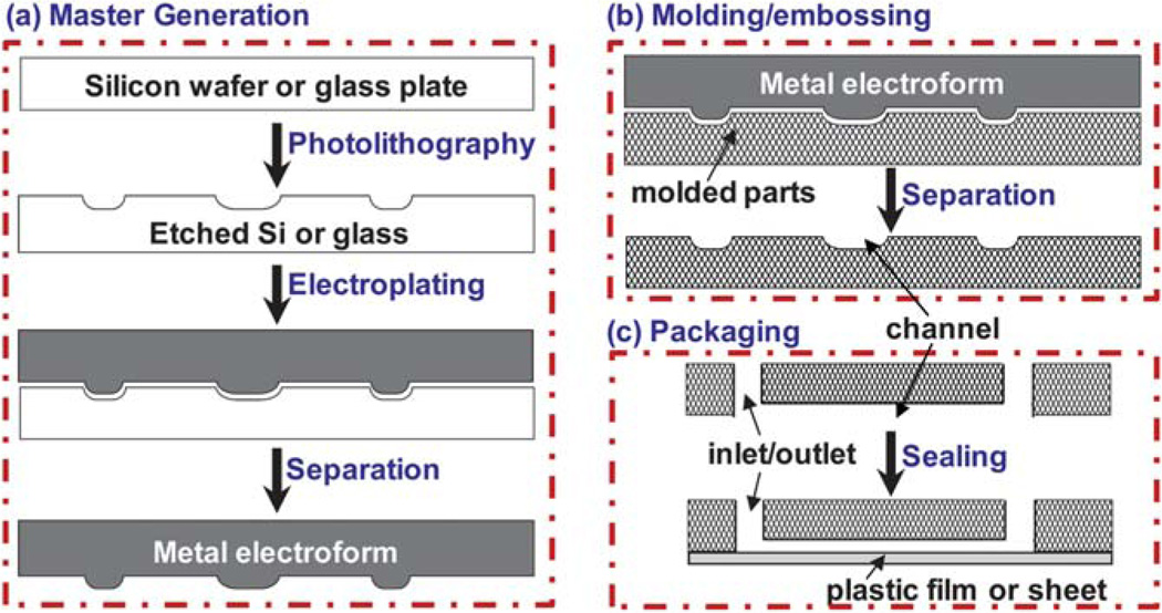
Fig. 1.
(a) The process of generating a master or molding die. A pattern of microfeatures (e.g. channels or chambers) is created in a silicon or glass substrate using photolithography. A metal mold (called electroform) is produced by electroplating on the patterned substrate. Note that the topology of the mold is exactly the opposite of the patterned silicon or glass substrate; a channel in the substrate becomes a ridge in the mold. (b) Plastic parts are fabricated using molding or embossing. The channels are in the direction out of the paper. Note that the topology of the plastic part is a negative image of the mold. Therefore, the plastic part has the exactly same shape as the patterned silicon or glass substrate. Repetitive molding would produce a large number of plastic parts without going through the photolithography steps for each individual device. (c) Packaging steps include drilling the inlet/outlet at the ends of each channel, followed by sealing the part with a plastic film or sheet. Shown in (c) is the molded part in (b) that is flipped vertically and then rotated 90° so that the channel is in the direction along the paper to show the inlet/outlet.

