Abstract
Ultra-small all-optical switches are of importance in highly integrated optical communication and computing networks. However, the weak nonlinear light-matter interactions in natural materials present an enormous challenge to realize efficiently switching for the ultra-short interaction lengths. Here, we experimentally demonstrate a submicron bidirectional all-optical plasmonic switch with an asymmetric T-shape single slit. Sharp asymmetric spectra as well as significant field enhancements (about 18 times that in the conventional slit case) occur in the symmetry-breaking structure. Consequently, both of the surface plasmon polaritons propagating in the opposite directions on the metal surface are all-optically controlled inversely at the same time with the on/off switching ratios of >6 dB for the device lateral dimension of <1 μm. Moreover, in such a submicron structure, the coupling of free-space light and the on-chip bidirectional switching are integrated together. This submicron bidirectional all-optical switch may find important applications in the highly integrated plasmonic circuits.
Miniaturization, integration and multifunctionalization of optical devices hold the key to increasing the integration densities in the next generation of photonic circuits. Surface plasmon polaritons (SPPs)1,2,3, propagating along the dielectric-metal interface with the capability to overcome the diffraction limit, are regarded as the promising candidate for significantly miniaturizing the optical devices. Thus, tremendous interests in SPPs have been attracted recently, and various passive and active plasmonic structures were proposed and demonstrated to realize ultra-small optical devices4,5,6,7,8,9,10,11,12,13,14,15,16. Among them, the ultra-small all-optical plasmonic switch involving nonlinear light-matter interactions is a key component for realizing highly integrated optical communication and computing networks. However, because of the weak nonlinear light-matter interactions in natural materials and the large loss of nanoscale-confined SPP modes in nano-metallic structures, realizing all-optical switches with high on/off switching ratios in ultra-small plasmonic structures is still an open challenge. Designing plasmonic structures with enhanced light-matter interactions therefore becomes extremely urgent, and it could open a route to effectively improve the device performances4,14,15.
In the past decade, considerable efforts have been made to design various metallic structures to realize all-optical plasmonic switches14,16,17,18,19,20,21,22,23,24,25,26,27,28. For example, by changing the imaginary part of the nonlinear optical materials' permittivities, the SPP propagation loss could be all-optically controlled in the coupling-decoupling structures16,17,18,19. The highest on/off switching ratio obtained was up to 6 dB for the device lateral dimension of about 11.4 μm18. However, in order to realize efficiently all-optical switching in these structures, the probe wavelengths have to be close to the absorption peaks of the optical materials (metal or dielectric)16,17,18,19. This greatly limits their applications because of the strong absorptions and the short SPP propagation lengths. Moreover, these switching processes happened during the single-pass propagation of SPPs (traveling waves) in the coupling-decoupling structures16,17,18,19, which allows individual photons to sample their environment for only one time. This makes the switching process not effective due to the weak light-matter interactions. Another direct way is to vary the real part of the optical materials' permittivities to change the effective refractive index of SPPs. This can bring about a spectral shift and nearly has no influence on the SPP propagation length in the plasmonic structures. Based on this principle, the SPP coupling processes in prism20,21,22,23 and grating24,25 structures were all-optically controlled efficiently. But these structures are bulky and difficult to be integrated into chips. Small structures, such as nanohole arrays (with the structure size of about 10 μm)26,27 and nano-antennas28, were also engaged to control SPPs. In these structures, only very small modulation depths (ΔT < 5%) were achieved because of the broad response spectra which behaved low sensitivity to the index variations of the surrounding medium. Moreover, they are not on-chip switching and thus are difficult to be integrated into chips, too. Recently, a compact asymmetric single slit (with lateral dimension of only about 2 μm) based on the resonator effect was experimentally demonstrated to efficiently control the SPPs on a chip14. In this work, the utilization of the resonator effect increased the nonlinear light-matter interaction length, which provided a strategy for improving the device performances, such as increasing the on/off switching ratio and shrinking the device size14. However, the nearly symmetric Lorenz-like response spectra with long decreasing tails in the single resonator make it difficult to further downscale the device sizes due to the relatively low sensitivity of the response spectra to the index variations29,30. Besides, in all the previous plasmonic structures14,16,17,18,19,20,21,22,23,24,25,26,27,28, only the SPPs propagating in one direction could be all-optically switched.
In the letter, an ultra-small asymmetric T-shape single slit composed of two detuned resonators coated with a nonlinear polymer film on a gold film is proposed to realize a submicron bidirectional all-optical switch. With the coupled-resonator effect, inverse and sharp asymmetric spectra as well as significant field enhancements (about 18 times that in the conventional slit case) emerge in the symmetry-breaking structure. This makes the response spectra extremely sensitive to the index variations of the surrounding medium29,30,31,32,33, which is favorable for the efficient all-optical switching of SPPs as well as for downscaling the device sizes. Compared with the previous absorption-type switches16,17,18,19, the nonlinear polymer film here is transparent to the probe light, so the requirement on the probe wavelength is not critical and the SPPs have much longer propagation lengths. By varying the real part of the polymer permittivities with a pump beam, both of the SPPs propagating in two opposite directions on the metal surface can be efficiently switched inversely at the same time, revealing a prospect of more functionalizations. Furthermore, it should be pointed out that the coupling of free-space light to SPPs and the on-chip bidirectional switching are integrated together in the same asymmetric T-shape single slit. This considerably shrinks the device size. Experimentally, an ultra-small bidirectional plasmonic switch with a lateral dimension of <1 μm and a high on/off switching ratios of >6 dB is achieved due to the enhancement of light-matter interactions. This submicron bidirectional plasmonic switch may find important applications in the highly integrated plasmonic circuits and also can be exploited to develop novel ultra-small active plasmonic devices, such as active SPP sources, active filters, and active dichroic splitters.
Results
Theoretical background
The proposed asymmetric T-shape single slit is schematically shown in Fig. 1. Similar structures were designed to study the transmission light in previous works33,34. Here, we mainly focus on the SPPs propagating along the front metal surface in the proposed structure. When p-polarized light (magnetic vector parallel to the slit) illuminates the structure from the back side, the SPPs will be generated and then propagate along the bottoms of the grooves. In each groove, the generated SPPs will be reflected back and forth between the metal steps of the groove and the nanoslit aperture, acting as a Fabry-Perot (FP) resonator5, as shown in Fig. 1. The electromagnetic field in the FP resonators can be scattered into SPPs on the front metal surface by the metal steps of the grooves. Meanwhile, these two FP resonators would affect and couple with each other at the nanoslit aperture. As a consequence, both of the FP resonator characteristics and the coupling effect would greatly influence the generated SPP intensities on the front metal surface, as shown in Fig. 1.
Figure 1. Schematic and geometric parameters of the asymmetric T-shape single slit.
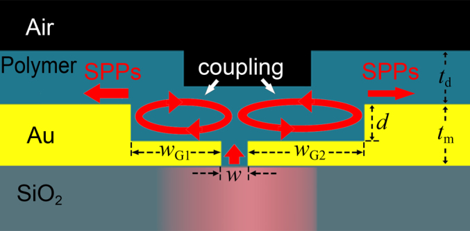
The symmetry-breaking structure comprises a conventional nanoslit (width of w) in immediate contacting with two grooves of detuned widths (wG1 and wG2) covered by a polymer film on a gold film.
To understand this complex generation process of SPPs in such an asymmetric T-shape single slit involving both of the resonator effect and the coupled-resonator effect, the nanoslit in immediate contacting with only one groove is investigated firstly, as shown by the inset in Fig. 2a. In the structure, the tight field confinement by the dielectric film can ensure a high reflectivity off the metal step of the groove33, while the reflectivity off the metal step of the nanoslit aperture is low. The calculated results of the SPP generation spectra (ηR for the right-propagating SPPs and ηL for the left-propagating SPPs) in the single-groove case for the groove width of wG = 630 nm are displayed in Fig. 2a (see Simulation methods). It is observed that the SPP generation spectra exhibit nearly symmetric Lorenz-like profiles with a bandwidth [full width at half maximum (FWHM)] of about ΔλFWHM ≈ 100 nm, corresponding to a low quality factor of about Q = 8. This is a typical response spectrum in the single optical resonator8,14,30, and the broad bandwidth is mainly owing to the low reflectivity off the metal step of the nanoslit aperture.
Figure 2. Simulation results in the single-resonator structure.
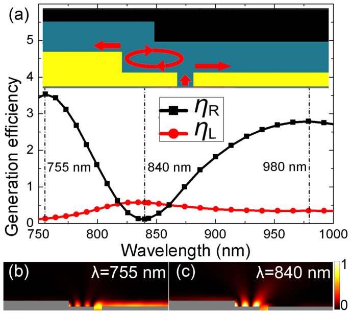
(a) SPP generation spectra with nearly symmetric Lorenz-like line shapes in the single resonator. Inset shows the schematic of the nanoslit with only one groove. The gold film thickness, the slit width, the groove depth, and the dielectric-film thickness are set to be tm = 250 nm, w = 200 nm, d = 150 nm, and td = 160 nm, respectively. Field distributions (|H|2) on the front metal surface for (b) λ = 755 nm and (c) λ = 840 nm. The gray parts denote the Au film.
In these symmetric spectral profiles, from the peak (corresponding to an “on” state) to the valley (corresponding to an “off” state), the wavelength separations are about 140 nm for the long wavelengths and about 85 nm for the short wavelengths. This indicates that the blue-shift (or red-shift) of the spectra should be about Δλ = 140 nm (or 85 nm) to realize a complete on-off switching. The corresponding field distributions (|H|2) at the peak and valley positions are displayed in Fig. 2b,c. At the off-resonant wavelength of λ = 755 nm, the field intensity in the resonator is weak, and the generated SPPs mainly propagate to the right direction with the intensity increased by about 4 times (Fig. 2b). This indicates that the left-propagating SPPs generated by the nanoslit are nearly completely reflected back by the FP resonator and then interference constructively with the right-going SPPs. On the contrary, the field intensity in the resonator becomes strong and the generated SPPs mainly propagate to the left direction at the resonant wavelength of λ = 840 nm (Fig. 2c). It should be stressed that the choice of these structure parameters is arbitrary, and that the geometry of the asymmetric T-shape slit can always be tuned to match the desired wavelength.
Next, the coupled-resonator effect is investigated in the asymmetric T-shape sing slit (inset in Fig. 3a), where the two resonators strongly affect and couple with each other at the nanoslit aperture. To observe the coupling influence, the generation spectra for wG1 = 550 nm and wG2 = 630 nm (the other parameters remaining unchanged) were calculated and the results are displayed in Fig. 3a. Clearly, it is observed that the SPP generation spectra become asymmetric, sharp and inverse in the symmetry-breaking structure. The generation efficiency varies sharply from the valley to the peak with only a small wavelength shift of about 22 nm (Fig. 3a), which is considerably smaller than that (Δλ = 140 nm or Δλ = 85 nm) in the single-resonator case. This reveals that the wavelength shift required for a completely on/off switching is significantly reduced. The corresponding field distributions at the peak and valley positions are displayed in Fig. 3b,c. At λ = 793 nm, the generated SPPs mainly propagate to the left direction (Fig. 3b). While, the generated SPPs mainly propagate to the right direction for λ = 815 nm (Fig. 3c). More importantly, it is noted that the SPP intensities in the corresponding FP resonators become much stronger (Fig. 3b,c), and they are about 3 times that in the single-resonator case and even about 18 times that in the conventional single-slit case (without grooves). The enhanced SPP intensities are attributed to the high reflectivity off the adjacent FP resonator at off-resonant wavelengths in the symmetry-breaking structure. This high reflectivity together with the high reflectivity off the metal step of the groove33 can excite strong trapped resonances with a high quality factor of about Q = 40 in the corresponding FP resonator31. Thus, the sharp and asymmetric spectra, usually termed as Fano profiles, result from the coupling of a narrow discrete resonance (strong resonance) and a broad spectrum (weak resonance)29,31,32. The strong trapped resonances allow individual photons to sample the environment for many times, which makes the Fano profiles become quite sensitive to the index variations of the environment29,32. The pronounced properties in the ultra-small symmetry-breaking structure, such as the small required wavelength shifts, the strong field enhancements, and the increased sensitivity to the index variations, can be exploitable in applications of optical switching14,29,32,33.
Figure 3. Simulation results in the asymmetric T-shape single slit.
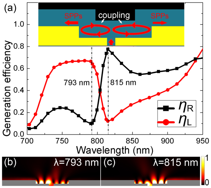
(a) Generation spectra in the asymmetric T-shape single slit for wG1 = 550 nm and wG2 = 630 nm. Inset shows the schematic of the asymmetric T-shape single slit with two detuned resonators. Distributions of the power flow on the front metal surface for (b) λ = 793 nm and (c) λ = 815 nm.
Experiments of submicron all-optical switching
To demonstrate the proposal experimentally, a compact asymmetric T-shape single slit was fabricated in a gold film on a glass substrate (see Fabrication methods). Fig. 4a shows the scanning electron microscopy (SEM) image of the asymmetric T-shape single slit. In the middle, there is a single 18-μm-long nanoslit. The lower half of the nanoslit is flanked by two shallow grooves to form the asymmetric T-shape slit, and the upper half of the nanoslit without the nanogroove acts as an in-chip reference. Figure 4b displays the details of the asymmetric T-shape single slit. The measured geometrical parameters of the asymmetric T-shape single slit are as follows: the slit width is about w = 100 nm; the groove depth is about d = 120 nm; and the width of the two resonators are about wG1 = 280 nm and wG2 = 600 nm. Note that the total lateral dimension of the asymmetric T-shape single slit is only 980 nm (Fig. 4b). Two decoupling gratings (period of about 410 nm and separation of about 26 μm) lying symmetrically on both sides of the nanoslit were merely designed to scatter the SPPs5,14. The whole structure was then spin coated with a 180-nm-thick photorefractive polymer film. This polymer film is a guest-host system: small molecules containing azobenzene chromophore14,35,36 are doped into a Polymethylmethacrylate (PMMA) polymer.
Figure 4. Experimental sample and all-optically switching processes.
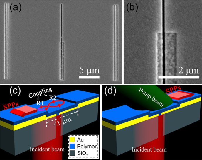
(a) SEM picture of the experimental structure. (b) Details of the asymmetric T-shape single slit. (c) and (d) Schematics of the bidirectional switching process in the asymmetric T-shape single slit coated with a polymer film.
In the experiment, the SPP generation spectra of the asymmetric T-shape single slit was first measured by changing the incident wavelengths without the pump light (see Measurement methods), and the results are displayed in Fig. 5a. Herein, the polymer film is transparent at these probe wavelengths14,35, so the SPP propagation loss is much smaller than that in the previous absorption-type switches16,17,18,19. It is observed that the generation spectra exhibit inverse and asymmetric response profiles, coinciding with the previous analysis. Next, a control (pump) laser beam (semiconductor laser, continuous wave) of p-polarization with the wavelength of 532 nm and a radius of about 100 μm was used to illuminate the structure from the front side at an angle of about 60° to the metal surface, as illustrated in Fig. 4d (see Measurement methods). The control beam wavelength is within the linear absorption band of the photorefractive polymer35, so the control light was absorbed and resulted in reorientations of the azobenzene molecules in a direction parallel to the slit14,35,36. As a result, the SPPs in the groove felt a refractive index (real part) quite different from that of the originally isotropic polymer with random molecule orientations. This index variation can bring about a shift of the SPP generation spectra in the asymmetric T-shape single slit. Figure 5b displays the measured SPP generation spectra with a pump intensity of about Ipump = 480 W/cm2 (the pump light is eliminated by a long pass filter in the detection). A large blue shift of about Δλ = 20 nm is obviously observed here. To verify the experimental results, we numerically simulated the SPP generation spectra in this case (see Simulation methods). It was found that the simulation spectra with the polymer index of nd = 1.58 and nd = 1.53 (Fig. 5c,d) well matched the experimental results without and with the pump light, respectively. This strongly supports our experiment. Here, the slight deviation from the simulation results is mainly owing to the fabrication defects of the sample (Fig. 4b).
Figure 5. SPP generation efficiencies for various incident wavelengths.
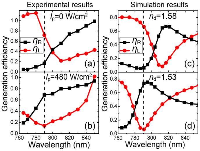
Experimental [(a) and (b)] and simulation [(c) and (d)] results of the SPP generation spectra in the asymmetric T-shape single slit without [(a) and (c)] and with [(b) and (d)] the pump light.
It is noted that the SPP generation efficiencies at λ = 790 nm for the opposite directions have great reversal under the pump beam, as denoted by the dashed lines in Fig. 5. To observe the reversal detailedly, the SPP generation efficiencies at the wavelength of λ = 790 nm were measured by varying the pump intensity, and the results are shown in Fig. 6a. Without the pump, the generation efficiency for the right-propagating SPPs (black line) is nearly at its minimum, and the generation efficiency for the left-propagating SPPs (red line) is nearly at its maximum. As the pump intensity increases, the generation efficiency for the right-propagating SPPs increases, while the generation efficiency for the left-propagating SPPs decreases, as shown in Fig. 6a. This reversal indicates that both of the SPPs in the opposite propagating directions are efficiently all-optically controlled inversely at the same time. This is a submicron bidirectional plasmonic switch, which can also perform as an active SPP source, active filter, and active dichroic splitter. Figures 6b and 6c show typical distributions of the scattered light from the decoupling gratings at λ = 790 nm with the pump intensities of Ipump = 0 W/cm2 and about Ipump = 480 W/cm2. For the upper parts of the two decoupling gratings (Fig. 6b,c), the signal intensities are nearly the same because the “isolated” nanoslit is a symmetric structure. Without the pump light, it is observed that the lower part of the right decoupling grating (ηR = 0.17, corresponding to an “off” state) is much darker than that of the left decoupling grating (ηL = 0.72, corresponding to an “on” state), which means that the SPPs mainly propagate to the left direction. With the pump light, the lower part of the right decoupling grating (ηR = 0.69, corresponding to an “on” state) becomes much brighter than that of the left decoupling grating (ηL = 0.14, corresponding to an “off” state), which means that the SPP propagation direction is changed from the left direction to the right direction. That is, the SPP propagating direction is completely varied by the pump beam, resulting in bidirectional plasmonic switching, as schematically illustrated in Fig. 4c,d. Thus, the submicron bidirectional plasmonic switch is experimentally realized with the on/off switching ratio of 10 × log10(0.69/0.17) ≈ 6.1 dB and 10 × log10(0.72/0.14) ≈ 7.1 dB for the lateral device dimension of <1 μm. Moreover, it is noted that the absolute change of the SPP generation efficiency is as large as about Δη = 0.58 in the submicron T-shape slit, which is a little greater than that in the symmetric single slit14.
Figure 6. SPP generation efficiencies for various pump intensities and CCD detected SPP intensities scattered from the decoupling gratings.
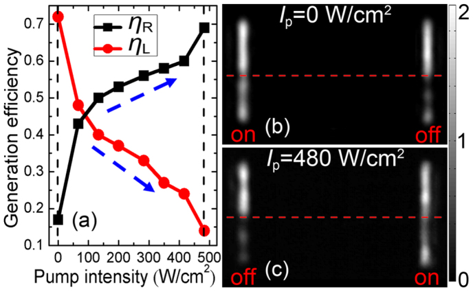
(a) SPP generation efficiencies at λ = 790 nm vs the intensity of the pump light. CCD detected SPP intensities scattered from the decoupling gratings for the pump intensities of (b) Ipump = 0 W/cm2 and (c) about Ipump = 480 W/cm2.
Discussion
The obtained high switching ratios of >6 dB in such a submicron plasmonic structure are mainly owing to two factors. One is that the SPPs are reflected back and forth in the FP resonators (not a single pass anymore), and the other is that the SPPs in the two detuned resonators couple with each other, resulting in strong trapped resonances (standing waves) in the symmetry-breaking structure. Both of these factors give rise to large field enhancements in the resonators, and thus the nonlinear light-matter interactions are dramatically enhanced in the submicron plasmonic structure. This is the guarantee of achieving such a high-performance all-optical switch in the submicron plasmonic structure. Several aspects of the submicron bidirectional all-optically switch can still be improved. For example, by using other fabrication methods to eliminate the sample roughness, such as the template stripping methods37,38, the on/off switching ratio can reach even higher values. Besides, a faster switching speed14 can be achieved by using other nonlinear molecules, such as PC molecules20 and J-aggregates26. At last, it should be pointed out that the sample parameters were designed to get the largest absolute change of the SPP generation efficiency (Δη = 0.58) as well as a relatively high switching ratio (>6 dB). Without considering the absolute change of the SPP generation efficiency, the on/off switching ratio can become much higher by optimizing the parameters of the asymmetric T-shape single slit14.
In summary, an asymmetric T-shape single slit coated with a photorefractive polymer film on the metal film was proposed to realize a submicron bidirectional all-optical plasmonic switch. Due to the coupled-resonator effect, the SPP generation spectra in the proposed structure exhibited inverse, sharp, and asymmetric line-shapes, resulting in that the wavelength shift required for the completely on/off switching was significantly reduced. Meanwhile, in the nano-resonators, the SPP intensities became about 18 times that in the conventional single-slit case (without grooves) because the strong trapped resonances occurred in the symmetry-breaking structure. Thus, the light-matter interactions were significantly enhanced and the sharp responses were quite sensitive to the index variation of the polymer. By varying the real part of the refractive index of the polymer film with a pump beam, both of the SPPs propagating in the opposite directions on the metal surface were efficiently controlled inversely at the same time. Experimentally, an ultra-small bidirectional plasmonic switch with the lateral dimension of <1 μm and large on/off switching ratios of >6 dB was achieved in the proposed structure. Moreover, the coupling of free-space light to SPPs and the on-chip bidirectional switching were integrated in the same asymmetric T-shape single slit. Therefore, this submicron bidirectional all-optical switch may find important applications in the highly integrated plasmonic circuits, performing as active SPP sources, active filters, active dichroic splitters, bidirectional modulators, and so on. It also reveals that the design of ultra-small plasmonic structures can provide a possibility for improving the performance of all-optical switches by enhancing the nonlinear light-matter interaction despite the very weak nonlinear optical processes in natural materials.
Methods
Simulation
The generation spectra of SPPs in the asymmetric T-shape single slit were calculated by using the commercial finite element (FEM) solver of COMSOL Multiphysics. In the simulations, the refractive index of the dielectric film was nd = 1.50, and the permittivity of the gold was calculated as a function of the wavelength using interpolation and was taken from the literature39. Here, a two-dimensional simulation model was used. The SPP generation efficiency (ηR for the right-propagating SPPs and ηL for the left-propagating SPPs) was defined as the quotient between the SPP intensities generated by the nano-slit with and without the groove.
Fabrication
The asymmetric T-shape single slit was fabricated using focused ion beams in a 250-nm-thick gold film, which was evaporated on a glass substrate with a 30-nm-thick titanium adhesion layer. Here, the thin Ti layer can make the gold film adhere to the glass substrate more tightly. The Ti layer added in the modeling will have little influence on the results. The reason is that both of the SPP generation and switching processes occur on the front surface of the gold film.
Measurement
Here, the whole structure was normally illuminated from the back side using a p-polarized laser beam (Ti:sapphire laser) with a radius of about 100 μm, which could ensure nearly uniform incident intensities over the slit (Fig. 4c). The generated SPPs propagated along the front metal surface and were then scattered by the decoupling gratings. The scattered light were collected by a long working distance objective (Mitutoyo 20× NA = 0.58) and then passed through a block to remove the strong light scattered from the middle nanoslit, so only the lights scattered from the two decoupling gratings are imaged onto a charge coupled device (CCD). The measured SPP generation efficiency was obtained from the quotient between the light intensities scattered from the lower and the upper parts of the decoupling grating (evaluated by integration over a spatial scale on the grating). In the switching process, in order to well focus the pump beam and easily adjust the pump and probe beams independently14, the pump beam was designed to illuminate the sample at an oblique incident angle from the front side.
Author Contributions
J.C. carried out the simulation and analysis. J.C. and Z.L. conceived the experiment. J.C. and X.Z. performed the experiments. J.C. wrote the main manuscript text, and Q.G. gave help guidance and discussions. All authors reviewed the manuscript.
Acknowledgments
This work was supported by the National Basic Research Program of China (Grants 2010CB923200, 2009CB930504, and 2013CB328704) and the National Natural Science Foundation of China (Grants 11204018, 11121091, 51172030, and 11134001).
References
- Barnes W. L., Dereux A. & Ebbesen T. W. Surface plasmon subwavelength optics. Nature 424, 824–830 (2003). [DOI] [PubMed] [Google Scholar]
- Ebbesen T. W., Genet C. & Bozhevolnyi S. I. Surface-plasmon circuitry. Phys. Today 61, 44–50 (2008). [Google Scholar]
- Gramotnev D. K. & Bozhevolnyi S. I. Plasmonics beyond the diffraction limit. Nat. Photon. 4, 83–91 (2010). [Google Scholar]
- MacDonald K. F. & Zheludev N. I. Active plasmonics: current status. Laser Photonics Rev 4, 562–567 (2010). [Google Scholar]
- Chen J. J., Li Z., Yue S. & Gong Q. H. Efficient Unidirectional Generation of Surface Plasmon Polaritons with Asymmetric Single-Nanoslit. Appl. Phys. Lett. 97, 041113 (2010). [Google Scholar]
- Nikolajsen T., Leosson K. & Bozhevolnyi S. I. Surface plasmon polariton based modulators and switches operating at telecom wavelengths. Appl. Phys. Lett. 85, 5833–5835 (2004). [Google Scholar]
- Gosciniak J. et al. Thermo-optic control of dielectric-loaded plasmonic waveguide components. Opt. Express 18, 1207–1216 (2010). [DOI] [PubMed] [Google Scholar]
- Chen J. J., Li Z., Yue S. & Gong Q. H. Ultracompact surface-plasmon-polariton splitter based on modulations of quasicylindrical waves to the total field. J. Appl. Phys. 109, 073102 (2011). [Google Scholar]
- Dicken M. J. et al. Electrooptic Modulation in Thin Film Barium Titanate Plasmonic Interferometers. Nano Lett. 8, 4048–4052 (2008). [DOI] [PubMed] [Google Scholar]
- Dickson W., Wurtz G. A., Evans P. R., Pollard R. J. & Zayats A. V. Electronically Controlled Surface Plasmon Dispersion and Optical Transmission through Metallic Hole Arrays Using Liquid Crystal. Nano Lett. 8, 281–286 (2008). [DOI] [PubMed] [Google Scholar]
- Cai W. S., White J. S. & Brongersma M. L. Compact, High-Speed and Power-Efficient Electrooptic Plasmonic Modulators. Nano Lett. 9, 4403–4411 (2009). [DOI] [PubMed] [Google Scholar]
- Dionne J. A., Diest K., Sweatlock L. A. & Atwater H. A. PlasMOStor: A Metal-Oxide-Si Field Effect Plasmonic Modulator. Nano Lett. 9, 897–902 (2009). [DOI] [PubMed] [Google Scholar]
- Temnov V. V. et al. Active magneto-plasmonics in hybrid metal-ferromagnet structures. Nat. Photon. 4, 107–111 (2010). [Google Scholar]
- Chen J. J., Li Z., Yue S. & Gong Q. H. Highly efficient all-optical control of surface-plasmon-polariton generation based on a compact asymmetric single slit. Nano Lett. 11, 2933–2937 (2011). [DOI] [PubMed] [Google Scholar]
- Zhang S. et al. Photoinduced handedness switching in terahertz chiral metamolecules. Nat. Commun. 3, 942 (2012). [DOI] [PubMed] [Google Scholar]
- MacDonald K. F., Sámson Z. L., Stockman M. I. & Zheludev N. I. Ultrafast active plasmonics. Nat. Photon. 3, 55–58 (2009). [Google Scholar]
- Pacifici D., Lezec H. J. & Atwater H. A. All-optical modulation by plasmonic excitation of CdSe quantum dots. Nat. Photon. 1, 402–406 (2007). [Google Scholar]
- Pala R. A., Shimizu K. T., Melosh N. A. & Brongersma M. L. A nonvolatile plasmonic switch employing photochromic molecules. Nano Lett. 8, 1506–1510 (2008). [DOI] [PubMed] [Google Scholar]
- Samson Z. L., MacDonald K. F. & Zheludev N. I. Femtosecond active plasmonics: ultrafast control of surface plasmon propagation. J. Opt. A: Pure Appl. Opt. 11, 114031 (2009). [Google Scholar]
- Sasaki K. & Nagamura T. Ultrafast wide range all-optical switch using complex refractive-index changes in a composite film of silver and polymer containing photochromic dye. J. Appl. Phys. 83(6), 2894–2900 (1998). [Google Scholar]
- Krasavin A. V., MacDonald K. F., Zheludev N. I. & Zayats A. V. High-contrast modulation of light with light by control of surface plasmon polariton wave coupling. Appl. Phys. Lett. 85, 3369–3371 (2004). [Google Scholar]
- MacDonald K. F., Krasavin A. V. & Zheludev N. I. Optical modulation of surface plasmon-polariton coupling in a gallium/aluminium composite. Opt. Commun. 278, 207–210 (2007). [Google Scholar]
- Samson Z. L. et al. Chalcogenide glasses in active plasmonics. Phys. Stat. Sol. RRL 4, 274–276 (2010). [Google Scholar]
- Rotenberg N., Betz M. & van Driel H. M. Ultrafast control of grating-assisted light coupling to surface plasmons. Opt. Lett. 33, 2137–2139 (2008). [DOI] [PubMed] [Google Scholar]
- Zhang X. P., Sun B. Q., Hodgkiss J. M. & Friend R. H. Ultrafast Optical Switching via Waveguided Gold Nanowires. Adv. Mater. 20, 4455–4459 (2008). [Google Scholar]
- Dintinger J., Robel I., Kamat P. V., Genet C. & Ebbesen T. W. Terahertz All-Optical Molecule-Plasmon Modulation. Adv. Mater. 18, 1645–1648 (2006). [Google Scholar]
- Wurtz G. A., Pollard R. & Zayats A. V. Optical bistability in nonlinear surface-plasmon polaritonic crystals. Phys. Rev. Lett. 97(5), 057402 (2006). [DOI] [PubMed] [Google Scholar]
- Abb M., Albella P., Aizpurua J. & Muskens O. L. All-optical control of a single plasmonic nanoantenna –ITO hybrid. Nano Lett. 11, 2457–2463 (2011). [DOI] [PubMed] [Google Scholar]
- Luk′yanchuk B. et al. The Fano resonance in plasmonic nanostructures and metamaterials. Nat. Mater. 9, 707–715 (2010). [DOI] [PubMed] [Google Scholar]
- Chen J. J. et al. Plasmonic Y–splitters of High Wavelength Resolution Based on Strongly–coupled–resonator Effects. Plasmonics 7, 441–445 (2012). [Google Scholar]
- Fedotov V. A., Rose M., Prosvirnin S. L., Papasimakis N. & Zheludev N. I. Sharp trapped-mode resonances in planar metamaterials with a broken structural symmetry. Phys. Rev. Lett. 99, 147401 (2007). [DOI] [PubMed] [Google Scholar]
- Chang W. S. et al. A Plasmonic Fano Switch. Nano Lett. 12(9), 4977–4982 (2012). [DOI] [PubMed] [Google Scholar]
- Chen J. J., Li Z., Yue S., Xiao J. H. & Gong Q. H. Plasmon-Induced Transparency in Asymmetric T-Shape Single Slit. Nano Lett. 12, 2494–2498 (2012). [DOI] [PubMed] [Google Scholar]
- Min Q. & Gordon R. Surface Plasmon Microcavity for Resonant Transmission through a Slit in a Gold Film. Opt. Express, 16(13), 9708–9713 (2008). [DOI] [PubMed] [Google Scholar]
- Zhang L. et al. Photorefractive properties of polyphosphazenes containing carbazole-based multifunctional chromophores. Polymer 49, 2107–2114 (2008). [Google Scholar]
- Chen J. J. et al. Efficient All-Optical Molecule-Plasmon Modulation Based on T-shape single slit. Plasmonics DOI 10.1007/s11468-012-9380-2 (2012). [Google Scholar]
- Nagpal P., Lindquist N. C., Oh S. H. & Norris D. J. Ultrasmooth patterned metals for plasmonics and metamaterials. Science 325(5940), 594–597 (2009). [DOI] [PubMed] [Google Scholar]
- Zhu X. L. et al. Ultrafine and smooth full metal nanostructures for plasmonics. Adv. Mater. 22(39), 4345–4349 (2010). [DOI] [PubMed] [Google Scholar]
- Johnson P. B. & Christy R. W. Optical constants of the noble metals. Phys. Rev. B 6, 4370–4379 (1972). [Google Scholar]


