Abstract
The benzyne functionalization of chemical vapor deposition grown large area graphene and graphite was performed using a mixture of o-trimethylsilylphenyl triflate and cesium fluoride that react with the carbon surface. The reaction requires at least 2 days of treatment before the appearance of Raman and energy-dispersive X-ray spectral signatures that verify modification. Raman spectra of modified graphene and graphite show a rich structure of lines corresponding to C=C-C, C-H, and low frequency modes of surface-attached benzyne rings.
1.Introduction
Graphene is a two-dimensional atomic-thin layer of carbon, in which the carbon atoms have sp2 hybridization and form a hexagonal lattice in perfect crystalline order having two carbon atoms per unit cell. Starting from the first publications [1-4], this remarkable material is in the focus of scientific interest because of unique properties and promising potential applications. Many applications of graphene became possible after chemical modification of this material [5-16]. The most common methods for graphene functionalization utilize graphene oxide (GO) [17]. GO can be produced from graphite by using a strong acids and oxidation agents. This material, compared to graphene, has a rather good solubility in water and contains hydroxyl, carboxyl and epoxy groups available for chemical modifications. At the same time, GO usually has a high level of disorder, is poorly conductive, and has difficulties with reduction to an original graphene state [18]. To overcome these limitations, graphene films having well defined and controllable surface and interface properties, will be important for both fundamental investigations and for practical applications of this material. The chemical stabilization and modification of electronic properties of large-scale graphene structures are critical points for graphene-based electron device fabrication.
Benzyne cycloaddition is one of many variants of graphene functionalization. It could be, for example, an efficient method for the modification of graphene towards composite materials with improved mechanical properties. There are the reports about previous successful incorporation of aromatic rings on surfaces of fullerenes and carbon nanotubes [19-21]. The only existing publication on the previous attempt of benzyne-based graphene modification [22] was focused on GO-based technique.
Our work details the investigation of benzyne [2+2] or [2+4] cycloaddition modification of epitaxial graphene and bulk graphite. The conditions of the reaction were simple and mild. The success of the reaction was confirmed by Raman spectroscopy and energy-dispersive X-ray (EDX) spectroscopy.
2. Chemical vapor deposition grown graphene
Our chemical vapor deposition (CVD) growth procedure was similar to the technique described in Refs. 23-25. As a catalytic substrate, we used 25 μm-thick Cu foil (Alfa Aesar #10950). Before growth, substrates were cleaned in acetic or nitric acid, and then rinsed in deionized water. After that, the substrates were loaded into a 1.5 in. quartz tube furnace (Thermo Blue Ray). Cu foils were heated to approximately 1050 0C under atmospheric pressure in the flow of Ar (1000 cubic centimeters per minute (SCCM)), and then were annealed for 30 min in Ar:H2 flow (Ar:H2=1000:500 SCCM). After annealing, graphene was grown at the same temperature and pressure in the flow of CH4:H2:Ar=100:500:1000 SCCM (growth time 15 min), then the foils were rapidly cooled to room temperature in about 1500 SCCM Ar flow.
For testing purposes, we used chemically treated and untreated graphene-coated Cu foils, highly ordered pyrolythic graphite (HOPG) of SPI-I type (Structure Probe Inc.), and transferred graphene from Cu to Si/SiO2 substrates. For the latter samples, we used a procedure similar to that of Refs. 23,26. For transfer to Si/SiO2 substrates, polymethyl methacrylate (PMMA) was spun-cast on the foils and then baked at 170 0C. Foils then were immersed in water solution of iron (III) chloride until Cu was completely etched out. Then we transferred the PMMA films with attached graphene on Si substrates having 300 nm CVD-grown SiO2 on top. Samples were then dried and the PMMA was dissolved in acetone. The graphene transferred to Si/SiO2 was rinsed in acetone, isopropanol, and in deionized water.
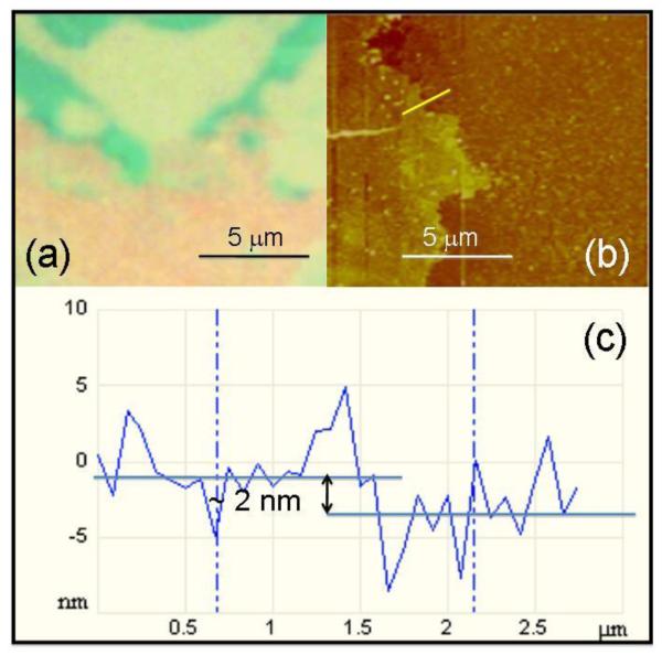
The transfer of graphene to Si/SiO2 substrate allows us to perform optical and atomic force microscopy testing of CVD-grown graphene. Figure 1(a) shows the typical optical image of CVD-grown graphene transferred to Si/SiO2 substrate. The image clearly shows the regions with a lower thickness, and the darker/greener “islands” where the growth of the next graphene layers has been started. In this respect, our results are consistent with those reported in the Ref.18 where it was reported that atmospheric-pressure CVD growth of graphene on Cu may lead to the formation of turbostratic graphene overlayers.
Figure 1.
Optical and AFM images of CVD-grown graphene used in our work. (a) Optical image of an edge of graphene layer transferred to Si/ 300 nm SiO2 substrate. The purple color corresponds to uncovered substrate, the light green-blue color corresponds to the thinner, major part of graphene, and the darker green “islands” show the areas where the next layer of graphene started to grow. (b) AFM image of one of edges of CVD-grown graphene transferred to Si/SiO2. Bright yellow line shows the direction of profile “cut” show in (c). (c) The AFM thickness profile of the edge of graphene shown in (b). Despite of the ocsillations caused the inherent roughness of the CVD-grown SiO2 layer, we see the thickness of graphene of about 2 nm.
We used the transferred graphene for determination of the thickness of our material. Figure 1(b) shows the results of atomic force microscopy (AFM) measurements of one of the flake edges of the Si/SiO2 transferred graphene. The surface of the CVD-grown SiO2 layer on Si is not uniform and has approximately 1 nm roughness that complicates thickness measurements. Despite this, we were able to measure the vertical profile of our samples near the flake edges. Our result (see Fig.1(c)) shows that the thickness of the major part of our CVD-grown graphene samples was about 2 nm corresponding to 2-3 monolayers.
3. Chemical reaction
3.1. The functionalization reaction: synthesis of benzyne-graphene and benzyne-graphite
Using standard procedures for the generation of benzyne species in reaction of carbon with o-trimethylsilylphenyl triflate (TMST) and cesium fluoride (CsF) [19-21], we mixed 0.131 mM of TMST and 0.393 mM of CsF in 1 ml of dry acetonitrile in Ar atmosphere. Then, the CVD-grown graphene sheets of about 1×1 cm2 on Cu substrates were added to the reaction mixture, and left for 1, 2, 4, 6, and 8 days. After these periods of time, the sheets were removed and washed thoroughly by deionized water, ethanol, acetonitrile and acetone, and then dried in gentle flow of Ar. The same procedure was performed on a 1×1 cm2 piece of highly oriented pyrolytic graphite (HOPG), which was left in the solution for 8 days. The possible structures of benzyne-graphene are shown in Fig.2. It is known from the literature [19-22, 27-29], that benzyne reactions with different forms of carbon (for example with fullerenes, carbon nanotubes, and graphene flakes obtained from graphene oxide) produce [2+2] or [2+4] cycloadditions. In fact, in our work we use the experiment of the work [22], using CVD-grown graphene instead of GO-made graphene.
Figure 2.
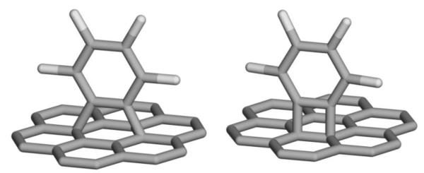
The possible structures of benzyne-graphene for (Left) [2+4] cycloaddition and (Right) [2+2] cycloaddition.. The gray color represents carbon atoms, the white color corresponds to H.
3.2. Selection of substrate for graphene samples
To investigate the properties of the fuctionalization reaction of CVD-graphene , we chose to explore graphene samples on Cu substrates in order to avoid transfer issues and improve accuracy in our subsequent testing. The additional operations required for graphene transfer to conventional Si/SiO2 substrates, combined with the use of more chemical agents and the risk of a longer exposition of graphene to ambient air (instead of pure Ar atmosphere), increases the risk of sample contamination. Working with as-grown graphene on Cu completely eliminates these issues.
4. Characterization techniques: Raman microscopy and energy-dispersive X-ray spectroscopy
We used Raman spectroscopy and Energy-Dispersive X-ray micro analysis (EDX) fluorescence spectroscopy for characterization of CVD-grown graphene and to characterize modifications introduced to graphene after chemical treatment.. In Raman measurements, we used the Horiba Jobin-Yvon Aramis grating micro-Raman spectrometer with a cooled CCD detector. For excitation, we used the second harmonic of Nd:YAG diode pumped laser (emission wavelength 532 nm, radiation power ~5 mW). Spatial resolution of Raman measurements in our experiments was about 2 μm.
We used EDX technique for monitoring of residual impurities, and for the verification of chemical modification of our graphene samples before and after chemical treatment. For this purpose we used the FEI Nova NanoSEM scanning electron microscope equipped with Genesis X-ray microanalysis system (EDAX/Ametek) with 10 keV electron beam energy.
5. Results of functionalization
5.1. Optical images of graphene before and after the treatment
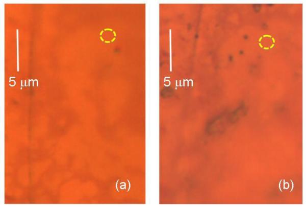
The optical images of the graphene sample before and after chemical modification using TMST with CsF are shown in Figure 3. After modification, the major part of sample appeared very similar to that before reactions, except at some points one can see the appearance of dark agglomerates of deposited material. In our Raman analyses, we selected the uniform areas away of these dark regions. The area from which the Raman spectra of the Figure 4 were taken, is indicated in Fig.2 by the yellow dashed circle.
Figure 3.
Optical images of the selected area of CVD-grown graphene on Cu substrate (a) before and (b) after 8 days of chemical treatment with TMST and CsF. The yellow dashed line encircled area shows the place from which we collected the Raman spectra shown in the Figure 4.
Figure 4.
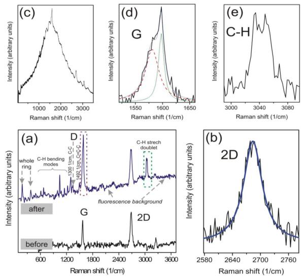
(Color online) Raman spectra of graphene and benzyne-graphene. (a) The spectra of a CVD-grown graphene sample taken from the same point before and after the 8 days-long functionalization treatment (the reaction of graphene with o-trimethylsilylphenyl triflate and CsF), with numerically extracted background from Cu substrate. For the discussion of new lines appearing in the spectrum after treatment see the text. (b): The shape of 2D line in our graphene sample before treatment: single Lorentzian at 2680 cm−1. (c):The raw spectrum of 8 days-treated graphene layer on Cu. (d):The part of the Raman spectrum of treated sample showing the result of benzyne attachment in the G-band region (encircled by the maroon dashed frame in (a)). The G-line of graphene (red dashed line, peak at ~1582 cm−1) overlaps with the C=C-C vibration of the attached benzyne ring (olive dotted line, peak at ~1595 cm−1). (e): The C-H stretching doublet near 3060 cm−1 appeared in the spectrum of treated sample (encircled by olive dashed frame in (a)). Excitation wavelength λexc=532 nm.
5.2. Raman spectra of benzyne-graphene
The Raman spectra for the selected area on graphene before and after treatment are shown in the Fig.4(a) after numerical removal of the background Raman spectrum of Cu substrate (see supporting information for details). The example of a raw as-measured spectrum of chemically-treated graphene with Cu background is shown in the Fig.4(c). The Raman spectra of untreated graphene (see the bottom curve in Fig. 4(a) ) show the typical set of lines: the G-line at 1582 cm−1, the 2D line at about 2680 cm−1, and 2D’ line at 3239 cm−1[30]. The 2D/G intensity ratio is about 1.3. It is worth noting that the position and the symmetric single-Lorentzian shape of 2D line (Fig.4(b)) as expected for monolayer graphene. At the same time, our AFM measurements show that the real thickness of graphene is ~2-3 monolayers (see supporting information for details). This result confirms the observations reported in the Ref.23, and indicates that we are most likely dealing with few-layer turbostratic graphene.
After chemical treatment of our sample, and after following cleaning of sample, the Raman spectra demonstrated significant modifications. The new lines occur at different frequency regions: the line at 1595 cm−1 (see the upper curve in Fig. 4(a)), the doublet at 3060 cm−1, the lines at 1492 cm−1, 1300 cm−1, 1230 cm−1, 1155cm−1, 1046cm−1, 996 cm−1, 673 cm−1, 386 cm−1, and at 187 cm−1 , and the graphene D line at 1340 cm−1[30]. It is important to mention, that our results are different from the results reported in Ref.22, where the only change actually observed in Raman spectra was just the increase of intensity in the defects-related D-line. In our case the Raman spectra shows the direct signatures of benzyne attached to graphene. In particular, the new narrow line at 1595 cm−1 (see Fig.4(d)) corresponds to the vibration of carbon atoms in the attached benzyne ring [31]. The line at 1492cm−1 (Fig.4(a)) also corresponds to attached benzyne, and represent a C=C-C aromatic ring stretching mode [31]. The mode at 1300 cm−1 corresponds to C-C vibrations (Fig.4(a)). The large number of the new lines in the Raman spectrum of benzyne-modified graphene represents the C-H modes. The doublet at 3060 cm−1 (Fig.1(e)) corresponds to the stretch C-H vibrations [31]. The lines at 1230, 1155, 1046, 996, and 673 cm−1 correspond to C-H in-plane and out-of-plane bending modes [31] (shown in Fig.4(a)). Finally, the very interesting region of low frequencies in benzyne-functionalized graphene, with the new lines at 190 and 378 cm−1 (see the upper curve of Fig.4(a)), should represent the vibrations of the whole (rather heavy) attached complex (including benzyne ring with additional hydrogen bonds) about its equilibrium position at the graphene surface. The lines at 190 and 378 cm−1 appear to be the first and second harmonics of the same mode. It is worth noting that the lines at 190 cm−1 and 378 cm−1 have significantly larger linewidths compared to the higher frequency “neighbor” at 673 cm−1.
5.3. EDX spectra of benzyne-graphene
Using EDX microanalysis, we monitored the changes of stoichiometry of our samples introduced during chemical treatment of graphene. We were not able to separate signals from regions with different graphene thicknesses, but had sufficient sensitivity to observe major changes in our samples due to chemical treatment and to assess the purity of chemically modified graphene.
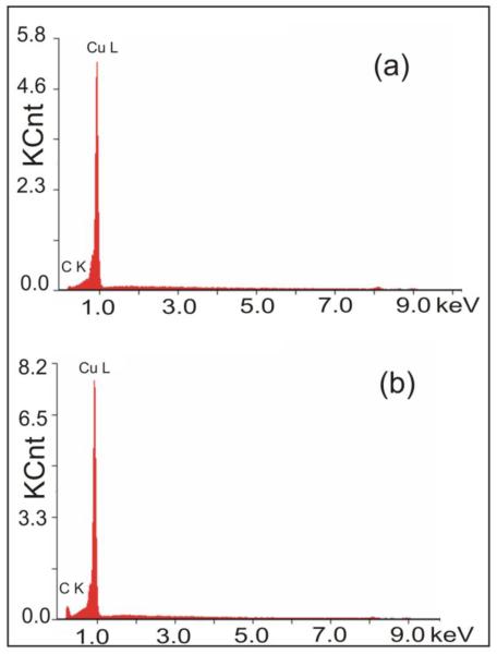
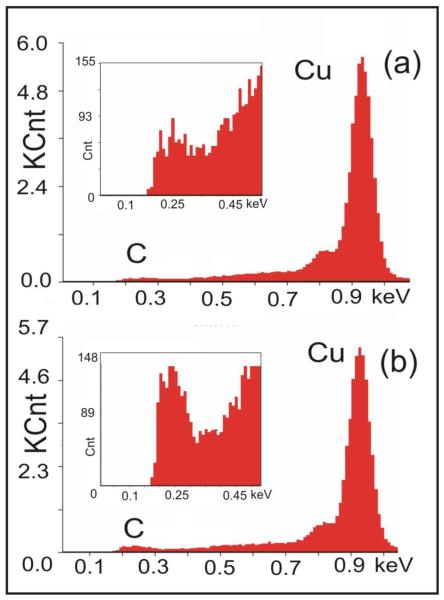
The energy-dispersive X-ray spectroscopy (EDX) spectra collected from the same lateral size (~3000 μm2) area of graphene on Cu substrate before and after the chemical treatment (in TMST and CsF), taken with the electron beam energy of 10 keV, are shown in the Figure 5. Fig. 5(a) shows the EDX spectrum of a graphene sample before chemical treatment. This is the the same sample which was investigated by Raman spectroscopy, and discussed in the Fig. 4. The EDX spectrum of our CVD-grown graphene sample before treatment (Fig. 5(a)) is practically identical to typical EDX spectra of (fully prepared for graphene growth) cleaned and annealed Cu substrates. The Cu substrates demonstrated similar EDX spectra with dominant Cu L peak, and small “tail” in the region between 0.9 and 0.2 keV, corresponding to remaining impurities in Cu, including oxygen (O K-line at 0.515 keV [32]) and carbon (C K-line at 0.246 keV, [32]). The CVD-deposited graphene layer itself is barely detectable by EDX. At the same time, the EDX spectra of the same graphene sample after chemical treatment (Fig. 5(b)) are distinctively different: the EDX signal corresponding to carbon K-line increased significantly. Therefore, EDX spectra (Figure 5(b)) confirm the successful result of chemical treatment via the increase of carbon contents in our samples.
Figure 5.
EDX spectrum (X-ray intensity in kilocounts (KCnt) vs. photon energy) taken from ~3000 μm2 area of the sample discussed in Figure S1, and in the Figure 1 of the main text, (a)-before, and (b)-after 8 days of chemical treatment in TMST and CsF. In EDX spectra the result of graphene functionalization is the increase of signal from carbon atoms (C K line), with no visible changes at any other photon energies. As soon as (a) and (b) shown in this fugure were not obtained in one experiment, one should look on the changes of the ratio of line intensities, ICK/ICuL.
EDX spectra also confirm the purity of our chemical treatment. We did not observe any visible changes in EDX signal from our samples after treatment at any emission energies other than the carbon K-line. Careful monitoring of EDX signal at the positions of oxygen (O K-line at 0.515 keV), nitrogen (N K-line at 0.384 keV,[32] may potentially occur from acetonitrile solvent during treatment), fluorine (F K-lin e [32] at about 0.68 keV) and Cs ( Cs L-line at 4.29 keV,[32] M-line at 0.565 keV,[32] may occur from CsF component of reaction), Si and S (Si K-line at 1.739 keV, S L-line near 0.16 keV and K-line near 0.23 keV ,[32] both may occur from TMST) does not show any increase of signal indicating that we do not see any detectable contamination of our treated graphene samples by compounds containing these elements at the level of sensitivity of EDX spectroscopy. This confirms the efficiency of our post-reaction cleaning procedure and supports the reliability of Raman results and its relation to functionalization, but not on a contamination, of our samples.
Figure 6 shows the details of the EDX spectra of as-grown graphene sample (Fig.6(a)), and the spectra of the part of the same sample after 8 days of reaction with the TMST and CsF (Fig.6(b)). As one can see, the functionalization reaction goes efficiently, and leads to the additional increase of the number of carbon atoms at the surface. This can be seen by comparing the intensity of C K-line in as-grown graphene (inset of the Fig.6(a) with the same after the first (inset of the Fig.6(b)).
Figure 6.
(a):The low energy part of EDX spectrum (X-ray intensity in counts or kilocounts (Cnt, KCnt) vs. photon energy) of the as-grown CVD graphene layer on Cu substrate around C K and Cu L X-ray emission lines [32], the inset represents the details of this spectrum near C K-line. Here the peak intensity of C K-line ICK~80 counts, the ratio of peak intensities of C K and Cu L lines ICK/ICuL~0.014. (b)-the EDX spectrum of the part of the same sample after 8 days of reaction in the mixture of o-trimethylsilylphenyl triflate with cesium fluoride; ICK~140 counts, ICK/ICuL~0.028. Both parts of the sample (the as-grown part, and the part after the reaction) were placed to the sample holder and measured in one experiment under the same electron beam focusing conditions; the same size/shape area of 4000 μm2 has been used for signal collection.
5.4. Reaction details: difference in interaction with oxidized and annealed non-oxidized Cu substrates
To further support our conclusions, we tested if the attachment of benzyne to the sample surface may happen to the surfaces not coated by carbon. We performed the reaction of TMST with CsF at the surface of uncoated Cu substrates including both fully oxidized Cu and Cu that had undergone typical pre-CVD growth annealing treatment. In the case of untreated/ insufficiently cleaned Cu substrates, we have seen addition of benzyne to oxidized, CuO-covered areas of substrates. At the same time, when our samples were properly etched (in nitric acid or in acetic acid) and annealed in the same way we used for growth of graphene (Cu foils were heated to approximately 1050 0C under atmospheric pressure in the flow of Ar (1000 cubic centimeters per minute (SCCM)), and then were annealed for 30 min in Ar:H2 flow (Ar:H2=1000:500 SCCM)), we did not observe products of reaction at the clean non-oxydized surfaces (See.Fig. 7). This test indicates that the observed changes in graphene samples were due to attachment of benzyne to graphene, and not to the Cu substrate.
Figure 7.
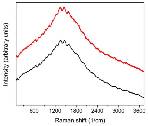
(Color online). The Raman spectrum from non-oxidized area of a clean etched and annealed surface of Cu substrate before (bottom, black curve) and after (top, red curve) 8 days of treatment in the mixture of TMST with CsF. No new lines or extra features in Raman spectra after the treatment. Excitation wavelength λexc=532 nm.
5.5. Duration of treatment
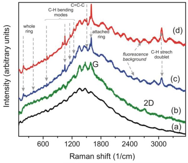
The attachment of benzyne to graphite or graphene surface in the mixture of TMST with CsF requires long reaction times. The Raman spectra of benzyne-graphene, obtained after different durations of treatment (Figure 8), show that the visible functionalization of graphene occured after 2 days of reaction. After a shorter time (24 hours) of reaction we did not observe any changes in Raman spectra of treated graphene. Larger amounts of attached benzyne required about a week-long treatments. This result, as well as the clear observation of signatures of the presence of attached benzyne, is different from to the results about reported in the Ref.22 benzyne functionalization of graphene after just 24 hours of treatment (with result samples having no C-H, C-C, and C=C-C lines in Raman spectra [31, 33-36]). In our case the intensity of defects-related D-line did not raise dramatically after chemical treatment (see Fig.4(a) and Fig.8). The possible reason of this rather unusual behavior of D-line is that the attachment of benzyne “heals” the defects, and “patches” the functionalization-broken bonds of graphene.
Figure 8.
(Color online) Raman spectra of pure cleaned annealed Cu substrate (a) and raw Raman spectra (without numerical removal of Cu background) of the CVD-grown few-layer graphene: (b) as-grown, (c) after 2 days of functionalization in the mixture of TMST with CsF, (d) after 6 days of functionalization. Increase of the duration of treatment leads to the increase of intensities of C-H and C=C-C lines, and to the increase of fluorescence signal, what indicates on the higher concentrations of attached benzyne rings after longer treatment durations. Excitation wavelength for Raman measurements λexc=532 nm.
Another important result of benzyne attachment to graphene is the appearance of broad fluorescence background in Raman spectra (see Fig.4(a) and Fig.8). We must emphasize that this result, as well as all other changes in Raman spectra discussed above, is not due to contamination of samples by byproducts or other components of reaction. We reproduced the same result after aggressive sequential cleaning of benzyne-graphene in deionized water, ethanol, acetone, and acetonitrile, rinsing benzyne-graphene samples twice for 2 minutes in each solvent, and repeating the whole procedure 3 times. In our experiments, the longer duration of treatment led to increase of intensities of benzyne-related Raman lines, and to the increase of fluorescent signal from benzyne-graphene
Figure 8 also illustrates the technique of numerical removal of Cu substrate background, showing the spectra of Cu substrate and the raw spectra of as-grown graphene and modified graphene (benzyne-graphene) on Cu. The appearance of fluorescence signal in Raman spectra of benzyne-graphene may indicate functionalization induced changes of graphene band structure [37], and/or participation of aromatic ring-localized electron states in the processes of radiative electron recombination.
5.6. Benzyne-functionalized graphite
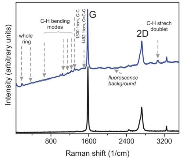
The robustness of the reaction of TMST with CsF at the carbon surface has been also tested at the surface of bulk highly oriented pyrolytic graphite (HOPG), using similar temperature, concentrations, and duration of reaction. As a result, we successfully fabricated benzyne-graphite. Figure 9 shows an optical image of the surface of HOPG after 8 days of treatment in the mixture of TMST and CsF. In order to rule out any possible role of layer edges or defects, we measured Raman spectra of benzyne-graphite selecting the most uniform and smooth areas of the sample surface away of cracks, defects, or irregularities on the surface. Figure 10 demonstrates the typical Raman spectrum of benzyne-graphite. The changes of the Raman spectrum due to functionalization are similar to what has been observed in benzyne-graphene: after addition on benzyne, one can see the C-H bending and stretching bands, attached aromatic ring-related C-C and C=C-C lines (correspondingly at 1300 cm−1 and 1492 cm−1) [31], the low frequency lines at 190 and 380 cm−1, and the appearance of spectrally-broad fluorescence signal. The attached ring-related line at 1595 cm−1 is hardly distinguishable near the strong G line of graphite.
Figure 9.
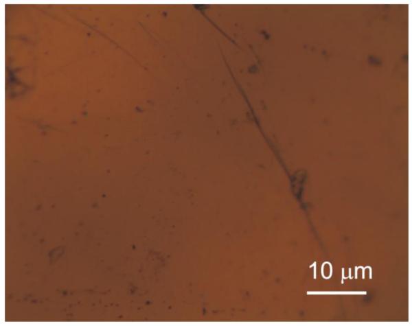
Optical image of benzyne-graphite surface after 8 days of treatment in the mixture of TMST and CsF.
Figure 10.
(Color online) Raman spectra of graphite (HOPG) before (black, bottom curve) and after 8 days-long treatment (blue, upper curve) in TMST and CsF. In the spectrum of treated material we see the same already discussed lines appearing as a result of reaction, and the visible fluorescence background increasing at the Stokes side of Raman spectrum. Excitation wavelength λexc=532 nm.
It is worth to point that the cleaning procedure of benzyne-graphite after functionalization reaction was similar to that described above for benzyne-graphene.
The modification of HOPG confirms that the functionalization reaction with TMST and CsF is successful on a flat carbon surface. It rules out the possible explanations of observed modification as results of involvement of substrate (for example, Cu) or defects of carbon layer.
6. Summary
We have performed the benzyne functionalization of epitaxial graphene and graphite. The functionalization of CVD-grown graphene and HOPG utilized the reaction of these materials with TMST and CsF under the mild conditions, reasonably low (below 100 0C) temperature and atmospheric pressure. The Raman spectra of the products of this reaction (benzyne-graphene and benzyne-graphite) show the direct signatures of attached benzyne: the ring line at 1595 cm−1,the lines at 1492 cm−1 (C=C-C vibrations) and 1300 cm−1 (C-C vibration), the C-H stretching and bending lines at different frequencies, the lines at 190 cm−1 and 380 cm−1, and the appearance of fluorescence from benzyne-graphene and benzyne-graphite. The success of graphene functionalization was confirmed by EDX spectroscopy. The demonstrated functionalization scheme may be important for creation of graphene-utilizing composite materials, and for graphene-based optoelectronic devices for the visible part of electromagnetic spectrum.
Supplementary Material
Acknowledgments
We acknowledge support from NSF (project #0925988), from the National Center for Research Resources (5P20RR016480-12) and the National Institute of General Medical Sciences (8 P20 GM103451-12) from NIH, and from the DOE Center for Integrated Nanotechnologies user support program (grants #U2008A061 and #RA2009B066). Sandia is a multiprogram laboratory operated by Sandia Corporation, a Lockheed Martin Company, for the United States Department of Energy’s National Nuclear Security Administration under contract DE-AC04 94AL85000.
Footnotes
Publisher's Disclaimer: This is a PDF file of an unedited manuscript that has been accepted for publication. As a service to our customers we are providing this early version of the manuscript. The manuscript will undergo copyediting, typesetting, and review of the resulting proof before it is published in its final citable form. Please note that during the production process errors may be discovered which could affect the content, and all legal disclaimers that apply to the journal pertain.
REFERENCES
- [1].Geim AK, Novoselov KS. The rise of graphene. Nature Materials. 2007;6(3):183–91. doi: 10.1038/nmat1849. [DOI] [PubMed] [Google Scholar]
- [2].Rao CNR, Sood AK, Subrahmanyam KS, Govindaraj A. Graphene: The new two-dimensional nanomaterial. Angew. Chem., Int. Ed. 2009;48(42):7752–77. doi: 10.1002/anie.200901678. [DOI] [PubMed] [Google Scholar]
- [3].Rao CNR, Sood AK, Voggu R, Subrahmanyam KS. Some Novel Attributes of Graphene. J. Phys. Chem. Lett. 2010;1(2):572–80. [Google Scholar]
- [4].Allen MJ, Tung VC, Kaner RB. Honeycomb carbon: a review of graphene. Chem. Rev. 2010;110(1):132–45. doi: 10.1021/cr900070d. [DOI] [PubMed] [Google Scholar]
- [5].Kushch SD, Kujunko NS, Tarasov BP. Platinum nanoparticles on carbon nanomaterials with graphene structure as hydrogenation catalysts. Russian J. General Chem. 2009;79(4):706–10. [Google Scholar]
- [6].Li Y, Tang L, Li J. Preparation and electrochemical performance for methanol oxidation of pt/graphene nanocomposites. Electrochem. Commun. 2009;11(4):846–9. [Google Scholar]
- [7].Kou R, Shao Y, Wang D, Engelhard MH, Kwak JH, Wang J, et al. Enhanced activity and stability of Pt catalysts on functionalized graphene sheets for electrocatalytic oxygen reduction. Electrochem. Commun. 2009;11(5):954–7. [Google Scholar]
- [8].Scheuermann GM, Rumi L, Steurer P, Bannwarth W, Mulhaupt R. Palladium Nanoparticles on Graphite Oxide and Its Functionalized Graphene Derivatives as Highly Active Catalysts for the Suzuki–Miyaura Coupling Reaction. J. Am. Chem. Soc. 2009;131(23):8262–70. doi: 10.1021/ja901105a. [DOI] [PubMed] [Google Scholar]
- [9].Li Y, Fan X, Qi J, Ji J, Wang S, Zhang G, et al. Gold nanoparticles–graphene hybrids as active catalysts for Suzuki reaction. Materials Research Bulletin. 2010;45(10):1413–8. [Google Scholar]
- [10].Ji J, Zhang G, Chen H, Wang S, Zhang G, Zang F, et al. Sulfonated graphene as water-tolerant solid acid catalyst. Chem. Sci. 2011;2(3):484–7. [Google Scholar]
- [11].Reddy ALM, Srivastava A, Gowda SR, Gullapalli H, Dubey M, Ajayan PM. Synthesis of nitrogen-doped graphene films for lithium battery application. ACS Nano. 2010;4(11):6337–42. doi: 10.1021/nn101926g. [DOI] [PubMed] [Google Scholar]
- [12].Cheng J, Tang L, Li J. Palladium nanoparticles-decorated graphene nanosheets as highly regioselective catalyst for cyclotrimerization reaction. J. Nanosci. Nanotechnol. 2011;11(6):5159–68. doi: 10.1166/jnn.2011.4173. [DOI] [PubMed] [Google Scholar]
- [13].Pyun J. Graphene Oxide as Catalyst: Application of Carbon Materials beyond Nanotechnology. Angew. Chem. Int. Ed. 2011;50(1):46–8. doi: 10.1002/anie.201003897. [DOI] [PubMed] [Google Scholar]
- [14].Gao Y, Ma D, Wang C, Guan J, Bao X. Reduced graphene oxide as a catalyst for hydrogenation of nitrobenzene at room temperature. Chem. Commun. 2011;47(8):2432–4. doi: 10.1039/c0cc04420b. [DOI] [PubMed] [Google Scholar]
- [15].Frank B, Blume R, Rinaldi A, Trunschke A, Schlogl R. Angew. Oxygen insertion catalysis by sp2 carbon. Chem. Int. Ed. 2011;50(43):10226–30. doi: 10.1002/anie.201103340. [DOI] [PubMed] [Google Scholar]
- [16].Bekyarova E, Sarkar S, Niyogi S, Itkis ME, Haddon RC. Advances in the chemical modification of epitaxial graphene. J. Phys. D.: Appl. Phys. 2012;45(15):154009, 1–9. [Google Scholar]
- [17].Dreyer DR, Park S, Bielawski CW, Ruoff RS. The chemistry of graphene oxide. Chem. Soc. Rev. 2010;39(1):228–40. doi: 10.1039/b917103g. [DOI] [PubMed] [Google Scholar]
- [18].Gomez-Navarro C, Weltz T, Bittner AM, Scolari M, Mews A, Burghard M, et al. Electronic Transport Properties of Individual Chemically Reduced Graphene Oxide Sheets. Nano Lett. 2007;7(11):3499–503. doi: 10.1021/nl072090c. [DOI] [PubMed] [Google Scholar]
- [19].Hoke SH, Molstad J, Dilettato D, Jay MJ, Carlson D, Kahr B, et al. Reaction of fullerenes and benzyne. J.Org. Chem. 1992;57(19):5069–71. [Google Scholar]
- [20].Nakamura Y, Takano N, Nishimura T, Yashima E, Sato M, Kudo T, et al. First Isolation and Characterization of Eight Regioisomers for [60] Fullerene–Benzyne Bisadducts. Org. Lett. 2001;3(8):1193–6. doi: 10.1021/ol0156547. [DOI] [PubMed] [Google Scholar]
- [21].Criado A, Gomez-Escalonilla MJ, Fierro JLG, Urbina A, Pena D, Guitian E, et al. Cycloaddition of benzyne to SWCNT: towards CNT-based paddle wheels. Chem. Commun. 2010;46(37):7028–30. doi: 10.1039/c0cc01907k. [DOI] [PubMed] [Google Scholar]
- [22].Zhong X, Jin J, Li S, Niu Z, Hu W, Li W, et al. Aryne cycloaddition: highly efficient chemical modification of graphene. Chem. Commun. 2010;46(39):7340–2. doi: 10.1039/c0cc02389b. [DOI] [PubMed] [Google Scholar]
- [23].Lenski DR, Fuhrer MS. Raman and optical characterization of multilayer turbostratic graphene grown via chemical vapor deposition. J. Appl. Phys. 2011;110(1):013720, 1–4. [Google Scholar]
- [24].Mattevi C, Kim H, Chhowalla M. A review of chemical vapour deposition of graphene on copper. J. Mater. Chem. 2011;21(10):3324–34. [Google Scholar]
- [25].Li X, Cai W, An J, Kim S, Nah J, Yang D, et al. Large-Area Synthesis of High-Quality and Uniform Graphene Films on Copper Foils. Science. 2009;324(5932):1312–4. doi: 10.1126/science.1171245. [DOI] [PubMed] [Google Scholar]
- [26].Reina A, Jia X, Ho J, Nezich D, Son H, Bulovic V, et al. Large area, few-layer graphene films on arbitrary substrates by chemical vapor deposition. Nano Lett. 2009;9(1):30–5. doi: 10.1021/nl801827v. [DOI] [PubMed] [Google Scholar]
- [27].Pellissier H, Santelli M. The use of arynes in organic synthesis. Tetrahedron. 2003;59(6):701–730. [Google Scholar]
- [28].Bhunia A, Reddy Yetra S, Biju AT. Recent advances in transition-metal-free carbon–carbon and carbon–heteroatom bond-forming reactions using arynes. Chem. Soc. Rev. 2012;41(8):3140–52. doi: 10.1039/c2cs15310f. [DOI] [PubMed] [Google Scholar]
- [29].Gampe CM, Carreira EM. Arynes and Cyclohexyne in Natural Product Synthesis, Angew. Chem. Int. Ed. 2012;51(16):3766–78. doi: 10.1002/anie.201107485. [DOI] [PubMed] [Google Scholar]
- [30].Ferrari AC, Meyer JC, Scardaci V, Casiraghi C, Lazzeri M, Mauri F, et al. Raman Spectrum of Graphene and Graphene Layers. Phys.Rev.Lett. 2006;97(18):187401, 1–4. doi: 10.1103/PhysRevLett.97.187401. [DOI] [PubMed] [Google Scholar]
- [31].Coates JP. Interpretation of Infrared Spectra, A Practical Approach. In: Meyers RA, editor. Encyclopedia of Analytical Chemistry. J. Wiley & Sons, Ltd; Chichester: 2000. pp. 10815–37. [Google Scholar]
- [32].Goldstein J, Newbury D, Joy D, Lyman C, Echlin P, Lifshin E, et al. Scanning Electron Microscopy and X-ray Microanalysis. Kluwer Academic/Plenum Publishers; New York: 2002. [Google Scholar]
- [33].Ferrari AC. Raman spectroscopy of graphene and graphite: Disorder, electron phonon coupling, doping and nonadiabatic effects. Solid State Communications. 2007;143(1-2):47–57. [Google Scholar]
- [34].Tan P, Dimovski S, Gogotsi Y. Raman scattering of non-planar graphite: arched edges, polyhedral crystals, whiskers and cones. Philos Transact A Math Phys Eng Sci. 2004;362(1824):2289–310. doi: 10.1098/rsta.2004.1442. [DOI] [PubMed] [Google Scholar]
- [35].Nemanich RJ, Solin SA. First- and second-order Raman scattering from finite-size crystals of graphite. Phys.Rev. B. 1979;20(2):392–401. [Google Scholar]
- [36].Chieu TC, Dresselhaus MS, Endo M. Raman studies of benzene-derived graphite fibers. Phys.Rev. B. 1982;26(10):5867–77. [Google Scholar]
- [37].Denis PA, Iribarne F. [2 + 2] Cycloadditions onto graphene. J. Mater. Chem. 2012;22(12):5470–7. [Google Scholar]
Associated Data
This section collects any data citations, data availability statements, or supplementary materials included in this article.


