Abstract
ZnO/TiO2 nanolaminates were grown on Si (100) and quartz substrates by atomic layer deposition at 200°C using diethylzinc, titanium isopropoxide, and deionized water as precursors. All prepared multilayers are nominally 50 nm thick with a varying number of alternating TiO2 and ZnO layers. Sample thickness and ellipsometric spectra were measured using a spectroscopic ellipsometer, and the parameters determined by computer simulation matched with the experimental results well. The effect of nanolaminate structure on the optical transmittance is investigated using an ultraviolet–visible-near-infrared spectrometer. The data from X-ray diffraction spectra suggest that layer growth appears to be substrate sensitive and film thickness also has an influence on the crystallization of films. High-resolution transmission electron microscopy images show clear lattice spacing of ZnO in nanolaminates, indicating that ZnO layers are polycrystalline with preferred (002) orientation while TiO2 layers are amorphous.
Keywords: ZnO/TiO2 nanolaminates, ALD, Transmittance, HRTEM
Background
ZnO is a low-cost and widely used semiconductor material with outstanding physical and chemical characteristics. At room temperature, the band gap and exciton binding energy of ZnO are 3.37 eV and 60 meV, respectively, both contributing to its extraordinary chemical and thermal stability. Thus, ZnO thin films exhibit magnificent applications in the manufacturing process of optoelectronic devices [1]. Also, being a promising semiconductor material that is transparent to visible light and has excellent optical transmittance, TiO2 is widely used in the synthesis of semiconductor photocatalysts, solar cell electrodes, and sophisticated electronic optical devices [2-5].
ZnO and TiO2 thin films, both with a wide band gap, high refractive index, high stability, and good catalysis, are suitable partners for multilayer nanostructures. On the one hand, TiO2 could serve as a buffer layer between ZnO and Si substrates. The lattice and thermal mismatches can be reduced, and the quality of ZnO films will be enhanced because TiO2 can inhibit the surface silicon atoms from plundering oxygen atoms in ZnO films [6,7]. Moreover, growing very thin ZnO films over a porous TiO2 electrode can improve the surface state and surface atomic mobility, so high-powered solar cells with better utilization efficiency can be produced [8]. There are also researches on ZnO/TiO2 multilayer mirrors at ‘water-window’ wavelengths with high reflectivity around 2.7 nm, indicating its potential in multilayer optics [9].
ZnO/TiO2 multilayers have been prepared by many techniques, such as chemical vapor deposition, pulsed laser deposition, and co-sputtering [10-12]. However, high-quality nanolaminate films require precisely controlled factors including interfacial roughness, interdiffusion between layers, layer-to-layer consistency, and conformality. Atomic layer deposition (ALD) is more powerful in preparing such multilayers than other techniques, which keeps the precursors separated during the reaction [13]. By sequentially dosing the surface with appropriate chemical precursors and then promoting surface reactions that are inherently self-limiting, the atomic layer control of film growth can be obtained. There has been a variety of publications on ALD-prepared ZnO or TiO2 films [14-17]. Thus, studies on ZnO/TiO2 multilayers prepared by ALD are of increasing importance in this field [18,19]. In this study, a series of ZnO/TiO2 nanolaminates were prepared by ALD. The optical and microstructural properties of ZnO/TiO2 were measured and compared by spectroscopic ellipsometry (SE), ultraviolet–visible-near-infrared (UV–vis-NIR) spectrometry, X-ray diffraction (XRD), and high-resolution transmission electron microscopy (HRTEM).
Methods
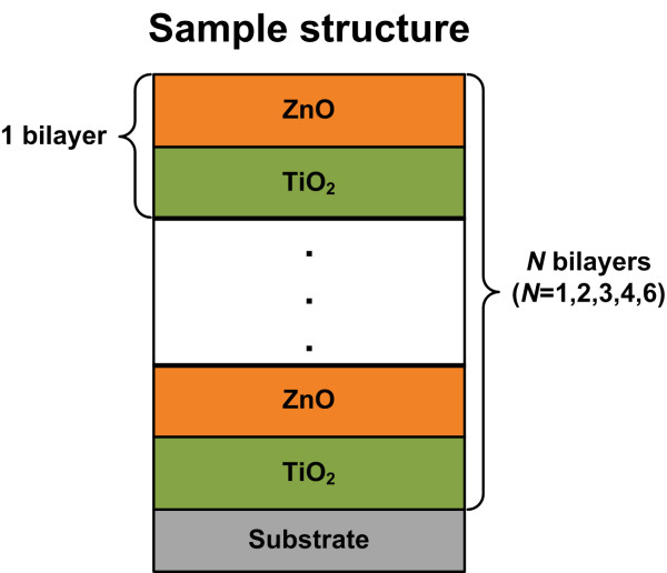
ZnO/TiO2 multilayers were deposited at 200°C using a BENEQ TFS-200 ALD reactor (Beneq Oy, Vantaa, Finland) on n-doped Si (100) (ρ = 1 to 10 Ω cm) and quartz substrates. ZnO films were deposited by alternating exposures to diethylzinc (DEZn) and deionized (DI) water, while TiO2 films were prepared using titanium isopropoxide (TTIP) and DI water as precursors. The TTIP and DEZn were held in stainless bubblers at 58°C and 18°C, respectively. The precursors were alternately introduced to the reactor chamber using high-purity N2 (>99.99%) as a carrier gas. An ALD cycle of TiO2 films consisted of 1.0-s TTIP dosing, 5.0-s N2 purge, 0.5-s DI water dosing, and 5.0-s N2 purge, while for ZnO films, the cycle is 0.5-s DEZn/2.0-s N2/0.5-s DI water/2.0-s N2. A schematic of five sample structures is given in Figure 1. Multilayers were prepared in depositing alternating layers of TiO2 and ZnO. Five samples contain one, two, three, four, and six ZnO/TiO2 bilayers, respectively. Each structure was deposited on Si and quartz substrates, respectively, so ten samples were prepared actually. The nominal film thickness for the multilayer was 50 nm.
Figure 1.
Schematic of physical models of ZnO/TiO2 nanolaminates grown by ALD.
The thicknesses of the multilayer were measured by spectroscopic ellipsometry (Sopra GES5E, SOPRA, Courbevoie, France) where the incident angle was fixed at 75° and the wavelength region from 230 to 900 nm was scanned with 5-nm steps. The optical transmission spectra were obtained using a UV spectrophotometer (UV-3100) in a wavelength range of 200 to 900 nm at room temperature in air. The crystal structures of the films were obtained using an X-ray diffractometer (D8 ADVANCE, Bruker AXS, Inc., Madison, WI, USA) using Cu Kα radiation (40 kV, 40 mA, λ = 1.54056 Å). High-resolution transmission electron microscopy and electron diffraction experiments were performed in a Philips CM200-FEG system operated at 200 kV. The specimens were prepared by mechanical polishing and dimpling, followed by Ar+ ion milling to electron transparency with 4.0-keV beam energy at an angle of 6° using a Gatan precision ion polishing system (Pleasanton, CA, USA).
Results and discussion
The experimental and fitted ellipsometric spectra of ZnO/TiO2 multilayer thin films were measured using the spectroscopic ellipsometer. For example, the experimental (open symbol) and calculated (solid line) ellipsometric spectra (cosΔ and tanψ) of samples 1 and 2 are presented in Figure 2a,b, respectively. It can be observed that the experimental and fitting curves match very well, with the accuracy of the regression (R2) greater than 0.998. Table 1 shows the layer thickness of the samples grown on Si substrate. As can be seen, total thicknesses for samples 1 to 5 are 51.14, 48.27, 46.92, 46.56, and 46.47 nm, respectively. The thickness of the first sample with single bilayer is very close to the nominal thickness of 50 nm. However, with the increase of TiO2 layers, the total thickness seems to be slightly thinner than the expected one, resulting from the reduced adsorption of DEZn on TiO2.
Figure 2.
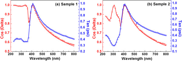
Comparison of experimental (open symbol) and calculated (solid line) ellipsometric spectra (cosΔ and tanψ). (a) Sample 1. (b) Sample 2.
Table 1.
The measured layer thickness of films with indexes 1 to 5 grown on Si by SE
| Sample ID | 1 | 2 | 3 | 4 | 5 |
|---|---|---|---|---|---|
| 1st layer-TiO2 |
18.85 |
8.85 |
5.87 |
4.23 |
2.73 |
| 1st layer-ZnO |
32.29 |
15.13 |
10.67 |
7.49 |
5.31 |
| 2nd layer-TiO2 |
|
8.97 |
4.81 |
4.15 |
2.47 |
| 2nd layer-ZnO |
|
15.32 |
10.37 |
7.46 |
5.28 |
| 3rd layer-TiO2 |
|
|
4.87 |
4.13 |
2.39 |
| 3rd layer-ZnO |
|
|
10.33 |
7.41 |
5.32 |
| 4th layer-TiO2 |
|
|
|
4.24 |
2.38 |
| 4th layer-ZnO |
|
|
|
7.45 |
5.28 |
| 5th layer-TiO2 |
|
|
|
|
2.38 |
| 5th layer-ZnO |
|
|
|
|
5.29 |
| 6th layer-TiO2 |
|
|
|
|
2.36 |
| 6th layer-ZnO |
|
|
|
|
5.28 |
| Total thickness (nm) | 51.14 | 48.27 | 46.92 | 46.56 | 46.47 |
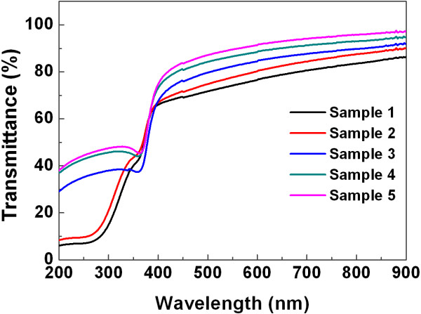
Transmittance spectrum for the samples grown on quartz is given in Figure 3. It can be found that the average transmittance over the entire visible wavelength range of 400 to 900 nm is more than 75%, while a strong absorption peak appears at 380 nm near the ultraviolet region. The transmittance increases with the decrease of the thickness of each TiO2 and ZnO layer. Moreover, the spectral transmittance value intensively decreases with the photon energy in the ultraviolet region. This is due to the strong absorption from fundamental band gap and high-energy critical point transitions. Since the emission band of ZnO is near the UV region, we can assume that the peak is a free-exciton absorption peak caused by oxygen vacancies in the film. It should be noted that the transmittances of samples 1 and 2 incline to 8% in the UV region, while the last three samples exhibit much higher transmittance, all between 30% and 40%. It suggests that the absorption in the UV region significantly depends on the sample structure. As the sample ID number increases, each ZnO layer in the sample becomes thinner, comparted by more TiO2 films, which prevents photon from being fully absorbed by ZnO, that is why the spectra drift upwards in the UV region [20-22].
Figure 3.
Transmittance spectrum of ZnO/TiO2 nanolaminates.
Figure 4a,b shows the XRD patterns of as-deposited ZnO/TiO2 nanolaminates on Si and quartz substrates, respectively. For sample 1 grown on Si substrate, XRD peaks appear at 2θ = 31.8° and 34.4°, which correspond with the spacing in (100) and (002) directions of the ZnO layer, respectively. However, only a small (002) peak is observed in sample 2, while no obvious peaks are observed in the other samples, which suggests that ZnO crystallization is suppressed with ZnO films getting thinner. So ZnO peaks could only be observed in the first two samples, where the thickness of a single ZnO layer is over 15 nm. On the other hand, a strong (002) peak along with (100) is observed for all the samples deposited on quartz. Strong (002) preferential orientation indicates the polycrystalline nature of the ZnO layer. ZnO grains are mainly (002)-aligned corresponding to the wurtzite structure of ZnO [23]. It suggests that ZnO layers within multilayers were grown on amorphous TiO2 layers and showed preferred (002) orientation. In addition, no TiO2 phase is detected in all samples. Taken together, these data suggest that layer growth appears to be substrate sensitive and film thickness also has an influence on the crystallization of films.
Figure 4.
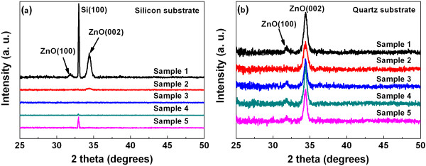
XRD spectra of ZnO/TiO2 nanolaminates. (a) Si substrate. (b) Quartz substrate.
For further investigation, the lattice constants of ZnO films grown on quartz are calculated according to Bragg’s law [24]:
| (1) |
where d is the interplanar spacing, λ is the X-ray wavelength which equals to 1.54 Å for Cu Kα radiation in this case, and θ is the scattering angle. Thus, the calculated values of d for ZnO (100) and (002) orientations are 2.8 and 2.6 Å, respectively. The grain size (D) of each ZnO layer can also be estimated using the Scherrer formula:
| (2) |
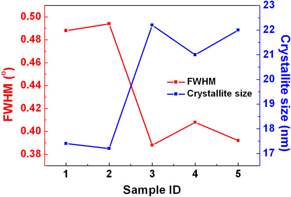
where D is the average crystallite size, K (=0.89) is a constant, λ is the wavelength (Å), β is the full width at half maximum (FWHM) of peaks, and θ is the Bragg angle [25]. Figure 5 shows the FWHM values and average grain sizes for ZnO (002) films on quartz substrates. It can be seen that the grain sizes for the first two samples are around 17 nm, while this value rises to 21 nm for the next three samples. The tendency coincides with the observed increase of transmittance above.
Figure 5.
FWHM of (002) peaks and average grain sizes for ZnO films deposited on quartz substrates.
The cross-sectional HRTEM image of the ZnO/TiO2 nanolaminate is presented in Figure 6. We took the second sample on Si substrate representatively for analysis. As shown in Figure 6a, the ZnO/TiO2 nanolaminate film is well prepared by ALD. The comparatively dark layers are ZnO layers, and the other two gray layers are TiO2 layers. In addition, a bright layer is also found between the first TiO2 layer and the substrate, which is a SiO2 interfacial layer, because the Si substrate is slightly oxidized during the ALD process. Furthermore, the thicknesses for TiO2 and ZnO layers are respectively detected, which are consistent with the results measured from SE. However, the thickness of the first TiO2 layer is slightly thinner than expected. It is mainly because growth rate was unsteady at the beginning of the ALD process. In addition, as referred above, the formed interfacial SiO2 layer between TiO2 and Si substrate will snatch oxygen atoms and decrease the growth rate of TiO2.
Figure 6.
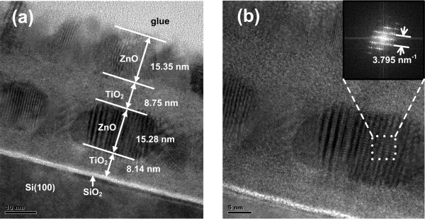
High-resolution TEM images (a, b) of the four-layer ZnO/TiO2 nanolaminate on Si (100) substrate. Inset shows FFT image of ZnO layer.
Crystallized ZnO shows clear lattice in the image, while a crystal structure could hardly be observed in TiO2 layers. Thus, TiO2 films are amorphous, that is why no diffraction peaks are observed in XRD. Fast Fourier transformation (FFT) image is shown in the HRTEM image (Figure 6b). The reciprocal lattice spacing can be identified to be 3.795 nm−1. As a result, the interplanar spacing is 2.6 Å, which is consistent with the calculated data for ZnO (002) orientation. Thus, it could be concluded that ZnO films grow on TiO2 along the (002) direction [26,27]. Besides, the crystallite size of ZnO film shown in TEM images is also very close to the values calculated from XRD peaks, further confirming the structure features of ZnO/TiO2 nanolaminate.
Conclusions
ZnO/TiO2 nanolaminates were grown on Si (100) and quartz substrates by ALD technique at 200°C. The optical and microstructural properties of samples with different numbers of bilayers are investigated. The thickness and growth rate of ZnO and TiO2 films are obtained using a spectroscopic ellipsometer, indicating the high accuracy of the ALD technique in controlling the growth of nanolaminates. The transmittance of multilayers in the visible wavelength increases gradually as the number of sample bilayers increases. The XRD spectra show that ZnO films grown on quartz are polycrystalline with preferred (002) orientation while TiO2 films are amorphous. The high-resolution TEM image for a representative sample shows clear lattice spacing along with the grain size of ZnO, confirming the structural properties of nanolaminated ZnO/TiO2 multilayers.
Competing interests
The authors declare that they have no competing interests.
Authors’ contributions
The experiments and characterization presented in this work were carried out by YZG, YG, and ZYY. The experiments were designed by YZG and HLL. YZG, YG, YZ, ZYY, QQS, SJD, HLL, and DWZ analyzed and discussed the results obtained from the experiments. The manuscript was prepared by YZG, and HLL helped with draft editing. All authors read and approved the final manuscript.
Contributor Information
Yu-Zhu Gu, Email: 10300720261@fudan.edu.cn.
Hong-Liang Lu, Email: honglianglu@fudan.edu.cn.
Yang Geng, Email: gengyang@fudan.edu.cn.
Zhi-Yuan Ye, Email: 10300720094@fudan.edu.cn.
Yuan Zhang, Email: zhangyuanzhy@fudan.edu.cn.
Qing-Qing Sun, Email: qqsun@fudan.edu.cn.
Shi-Jin Ding, Email: sjding@fudan.edu.cn.
David Wei Zhang, Email: dwzhang@fudan.edu.cn.
Acknowledgments
This work is supported by the Important National Science & Technology Specific Projects (no. 2011ZX02702-002), the National Natural Science Foundation of China (no. 51102048), the SRFDP (no. 20110071120017), and the Independent Innovation Foundation of Fudan University, Shanghai.
References
- Pandis C, Brilis N, Tsamakis D, Ali HA, Krishnamoorthy S, Iliadis AA. Role of low O2 pressure and growth temperature on electrical transport of PLD grown ZnO thin films on Si substrates. Solid State Electron. 2006;50:1119–1123. doi: 10.1016/j.sse.2006.04.025. [DOI] [Google Scholar]
- Marci G, Augugliaro V, López-Munoz MJ, Martín C, Palmisano L, Rives V, Schiavello M, Tilley RJD, Venezia AM. Preparation characterization and photocatalytic activity of polycrystalline ZnO/TiO2 systems. J Phys Chem. 2001;105:1026–1032. [Google Scholar]
- Gratzel M. Photoelectrochemical cells. Nature. 2001;414:338–344. doi: 10.1038/35104607. [DOI] [PubMed] [Google Scholar]
- Greene LE, Law M, Tan DH, Montano M, Goldberger J, Somorjai G, Yang P. General route to vertical ZnO nanowire arrays using textured ZnO seeds. Nano Lett. 2005;5:1231–1236. doi: 10.1021/nl050788p. [DOI] [PubMed] [Google Scholar]
- Cui Y, Du H, Wen L. Doped-TiO2 photocatalysts and synthesis methods to prepare TiO2 films. J Mater Sci Technol. 2008;24:675–689. doi: 10.1179/174328408X270301. [DOI] [Google Scholar]
- Zhang Y, Zhang LD, Mo CM, Li YH, Yao LZ, Cai WL. Synthesis, microstructure and optical absorption of coatings with doping of nano-TiO2 for protection against ultraviolet irradiation. J Mater Sci Technol. 2000;16:277–280. [Google Scholar]
- Mane RS, Lee WJ, Pathan HM, Han SH. Nanocrystalline TiO2/ZnO thin films: fabrication and application to dye-sensitized solar cells. J Phys Chem B. 2005;109:24254–24259. doi: 10.1021/jp0531560. [DOI] [PubMed] [Google Scholar]
- Roh SJ, Mane RS, Min SK, Lee WJ, Lokhande CD, Han SH. Achievement of 4.51% conversion efficiency using ZnO recombination barrier layer in TiO2 dye-sensitized solar cells. Appl Phys Lett. 2006;89:253512–253514. doi: 10.1063/1.2410240. [DOI] [Google Scholar]
- Kumagai H, Tanaka Y, Murata M, Masuda Y, Shinagawa T. Novel TiO2/ZnO multilayer mirrors at ‘water-window’ wavelengths fabricated by atomic layer epitaxy. J Phys Condens Matter. 2010;22:474008. doi: 10.1088/0953-8984/22/47/474008. [DOI] [PubMed] [Google Scholar]
- Jin C, Kim H, Jungkeun L, Lee J, Lee C. Fabrication and optical emission of TiO2-sheathed ZnO nanowires. J Nanosci Nanotechnol. 2012;12:1318–1322. doi: 10.1166/jnn.2012.4649. [DOI] [PubMed] [Google Scholar]
- Zhao L, Han M, Liang SH. Photocatalytic activity of TiO2 films with mixed anatase and rutile structures prepared by pulsed laser deposition. Thin Solid Films. 2008;516:3394–3398. doi: 10.1016/j.tsf.2007.10.102. [DOI] [Google Scholar]
- García-Ramírez E, Mondragón-Chaparro M, Zelaya-Angel O. Band gap coupling in photocatalytic activity in ZnO-TiO2 thin films. Appl Phys A. 2012;108:291–297. doi: 10.1007/s00339-012-6890-x. [DOI] [Google Scholar]
- George SM. Atomic layer deposition: an overview. Chem Rev. 2010;110:111–131. doi: 10.1021/cr900056b. [DOI] [PubMed] [Google Scholar]
- Pung SY, Choy KL, Hou XH, Shan CX. Preferential growth of ZnO thin films by the atomic layer deposition technique. Nanotechnology. 2008;19:435609. doi: 10.1088/0957-4484/19/43/435609. [DOI] [PubMed] [Google Scholar]
- Li QC, Kumar V, Li Y. Fabrication of ZnO nanorods and nanotubes in aqueous solutions. Chem Mater. 2005;17:1001–1006. doi: 10.1021/cm048144q. [DOI] [Google Scholar]
- Carcia PF, McLean RS, Reilly MH. High-performance ZnO thin-film transistors on gate dielectrics grown by atomic layer deposition. Appl Phys Lett. 2006;88:123509–123511. doi: 10.1063/1.2188379. [DOI] [Google Scholar]
- Shan CX, Hou XH, Choy KL. Corrosion resistance of TiO2 films grown on stainless steel by atomic layer deposition. Surf Coat Technol. 2008;202:2399–2402. doi: 10.1016/j.surfcoat.2007.08.066. [DOI] [Google Scholar]
- Hussin R, Choy KL, Hou XH. Enhancement of crystallinity and optical properties of bilayer TiO2/ZnO thin films prepared by atomic layer deposition. J Nanosci Nanotechnol. 2011;11:8143–8147. doi: 10.1166/jnn.2011.5086. [DOI] [PubMed] [Google Scholar]
- Sanjo Y, Murata M, Tanaka Y, Kumagai H, Chigane M. In: Synthesis and Photonics of Nanoscale Materials VIII. Conference on Synthesis and Photonics of Nanoscale Materials VIII: January 24–25 2011; San Francisc. Geohegan DB, Dubowski JJ, Trager F, editor. Bellingham: SPIE; 2011. Atomic layer deposition of amorphous TiO2/ZnO multilayers for soft x-ray coherent optics. 79220L. [Google Scholar]
- Gao F, Yu KM, Mendelsberg RJ, Anders A, Walukiewicz W. Preparation of high transmittance ZnO: Al film by pulsed filtered cathodic arc technology and rapid thermal annealing. Appl Surf Sci. 2011;257:7019–7022. doi: 10.1016/j.apsusc.2011.03.013. [DOI] [Google Scholar]
- Lu WL, Hung PK, Hung CI, Yeh CH, Houng MP. Improved optical transmittance of Al-doped ZnO thin films by use of ZnO nanorods. Mater Chem Phys. 2011;130:619–623. doi: 10.1016/j.matchemphys.2011.07.034. [DOI] [Google Scholar]
- Oloomi SAA, Saboonchi A, Sedaghat A. Effects of thin film thickness on emittance, reflectance and transmittance of nano scale multilayers. Int J Phys Sci. 2010;5:465–469. [Google Scholar]
- International Centre for Diffraction Data. Powder diffraction file, data card 5–644. 3c PDS. http://www.icdd.com.
- Bragg WH. The distribution of the electrons in atoms. Nature. 1915;95:344. [Google Scholar]
- Warren BE. X-ray Diffraction. New York: Dover; 1990. [Google Scholar]
- Greene LE, Law M, Goldberger J, Kim F, Johnson JC, Zhang Y, Saykally RJ, Yang P. Low-temperature wafer-scale production of ZnO nanowire arrays. Angew Chem Int Ed. 2003;42:3031–3034. doi: 10.1002/anie.200351461. [DOI] [PubMed] [Google Scholar]
- Hsu YF, Djurisic AB, Tam KH, Cheung KY, Chan WK. Fabrication and characterization of ZnO/TiOx nanoscale heterojunctions. J Crystal Growth. 2007;307:348–352. doi: 10.1016/j.jcrysgro.2007.07.010. [DOI] [Google Scholar]


