Abstract
Control of the motion of domain walls in magnetic nanowires is at the heart of various recently proposed three-dimensional (3D) memory devices. However, fabricating 3D nanostructures is extremely complicated using standard lithography techniques. Here we show that highly pure 3D magnetic nanowires with aspect-ratios of ~100 can be grown using focused electron-beam-induced-deposition. By combining micromanipulation, Kerr magnetometry and magnetic force microscopy, we determine that the magnetisation reversal of the wires occurs via the nucleation and propagation of domain walls. In addition, we demonstrate that the magnetic switching of individual 3D nanostructures can be directly probed by magneto-optical Kerr effect.
Recently, intense research carried out on controlling the motion of domain walls (DWs) in magnetic nanowires (NWs) has led to the development of memories based on this concept1,2,3,4,5. To make these devices commercially viable, their storage capacity has to be substantially increased, requiring the extension of these concepts into the third dimension1,6. The paradigmatic example proposed for a device based on 3D magnetic NWs is the vertical racetrack memory1, where U-shaped NWs normal to the substrate act as shift registers for DWs which move up and down by applying electrical currents. However, whereas the two-dimensional (2D) version of this memory and other functional NW devices are a reality, their 3D realisation faces great challenges using similar lithography methods. Most techniques more suited for the growth of vertical NWs, such as electrodeposition, cannot grow complex 3D geometries, and the characterisation of single nanostructures requires either dissolving the membrane where the NWs have been grown, followed by dispersing the NWs on a substrate for subsequent characterisation7,8, or sophisticated contact strategies9,10. Here, we use focused electron beam-induced-deposition (FEBID) to grow high aspect-ratio functional 3D NWs. FEBID is a nanolithography technique consisting of the local chemical-vapour-deposition of a gas adsorbed on a substrate, where molecules are decomposed by the interaction with a focused beam of keV-range electrons11,12. It can be considered as a “direct writing” nanolithography technique, needing neither resists nor templates, which gives it unique properties for the fabrication of complex 3D nanostructures13. For the growth of magnetic NWs, we have used Co2(CO)8. We previously showed that 2D FEBID structures with up to 95% Co can be deposited using this gas precursor, when the growth is carried out at the precursor-limited-regime14. This contrasts with most FEBID materials, where the metallic content is typically not higher than 30–40%. In addition, we proved that nanostripes (2D-NWs with rectangular section) based on this material present good DW conduit properties15. Recent works show that functional 2D Co deposits can be fabricated at high resolutions16,17. In this work, we fabricate 3D cobalt NWs by FEBID, at the cross-over between the electron- and precursor- limited regime. Under these growth conditions, high aspect-ratio 3D NWs are grown, which present high metallic content, low roughness and functional magnetic properties.
Results
Growth of 3D magnetic nanowires
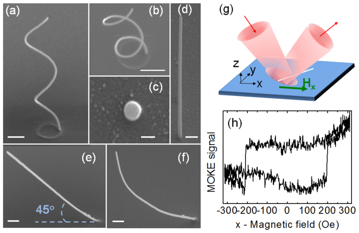
To exemplify the potential of FEBID to create 3D nano-devices, figures 1(a) and (b) show scanning electron microscopy (SEM) images of a two-loop cobalt nano-spiral, erected a few microns above the substrate. Figures 1(d) and (e) show two straight 3D-NWs similar to those studied in this work. They are 4–12 μm long, with a circular cross section (see figure 1(c)), and diameters Ø = 100 ± 25 nm. The NWs can be fabricated at any angle with respect to the substrate plane18. For these dimensions, after optimising growth parameters such as roughness, purity, homogeneity and minimum residual parasitic deposit, we obtained NWs with approximately 85% cobalt content, with the rest being carbon and oxygen. The Co content is remarkably higher than previous studies, where percentages of about 40% were reported for NWs with similar diameters to those studied here19,20. For more details about growth parameters and strategy see the methods section.
Figure 1. 3D magnetic nanostructures grown by FEBID.
(a) and (b) Different views of a double-loop nano-spiral. (c) Top-view of a straight NW. (d) and (e) Lateral view of NWs grown at 0 and 45 degrees, respectively, to the substrate plane. (f) Curved NW after MOKE measurements. The scale bar is 500 nm in all images, except in (c), where it is 100 nm. (g) Sketch of the experimental configuration used to obtain MOKE hysteresis loops of 3D-NWs at 45 degrees. (h) MOKE hysteresis loop of a 3D wire.
Direct magnetometry on single 3D nanowires
To characterise the wires we have used spatially-resolved magneto-optical Kerr effect (MOKE), which has proved to be an invaluable tool to study the magnetic switching of laterally-patterned nanomagnets2,4,5,15,17. Previously, all measurements had been performed on 2D structures; here we directly probe suspended 3D-NWs. Figure 1(g) shows the experimental configuration used. A laser spot is focused on an area of ~5 μm in diameter, over a NW grown at 45 degrees to the substrate (as the one in figure 1(e)). The incident and final angle of the laser beam with the substrate is 45 degrees. A magnetic field is applied in the plane of the film, along the projection of the NW axis on the substrate, referred to from now on as the x-direction. More details about the experimental setup can be found in ref. 21. Using simple arguments, the magnetic moment μ probed by MOKE can be estimated. MOKE is a surface magnetometry technique, where only the top ~20 nm, corresponding to the penetration depth of the light, contribute to the signal22,23. For a Ø = 100 nm wire oriented perpendicular to the substrate, the corresponding volume results in μ ≈ 2 × 10⁻¹³ emu, below the sensitivity of our system. On the other hand, for a μm-long tilted NW, μ ≈ 10−11 emu, well within the resolution limits of MOKE measurements on 2D nanostructures. Thus, to perform this type of MOKE measurements, a technique capable of growing tilted 3D-NWs, such as FEBID, is required.
Figure 1(h) shows a MOKE hysteresis loop for a single 3D-NW, obtained by averaging 1000 individual loops. Together with the standard sources of noise existing in MOKE experiments21, a 3D nanostructure produces a large amount of diffusive scattering when light is reflected, and a strong mechanical noise is generated by the vibration of the wires, making these measurements far more challenging than those on flat nanostripes. In order to minimise these effects, experiments were performed by focusing the laser close to the base of the NWs, where the signal-to-noise ratio is maximum (figure S1 in supplementary materials shows the evolution of the MOKE signal in 3D-NWs when the laser spot is placed on different points along the x-direction). By performing such measurements, as in figure 1(h), we observed square hysteresis loops, with coercivities (for fields applied along the x-direction) corresponding to a few hundred Oersted. These measurements constitute direct evidence of the 3D magnetic functionality of the wires.
Figure 1(f) shows the NW previously imaged in 1(e), after being measured by MOKE for several minutes, where the upper part is bent with respect to its initial direction. When probing a NW, the laser provides a maximum power density per unit length of 10 W/m, which in the case of 2D wires is efficiently dissipated by the substrate. However, we observed that for 3D-NWs only the ~2–3 μm long fragment of the wire closest to the substrate can dissipate this amount of heat quickly enough to avoid deformation. In order to prevent this effect, 3D-MOKE experiments were performed with the laser focused at the base of the wire, and minimising the exposure time, which eliminated any visible damage.
Micromanipulation and magnetometry on felled nanowires
In order to consider FEBID-Co NWs as future building blocks of 3D nanomagnetic architectures, the reversal mechanism of the magnetisation has to be well understood and controlled. The squareness observed for the MOKE loops of 3D-NWs suggests that they are in a single domain state at zero field. Also, the sharp transitions between saturated states, even after hundreds of averages, suggest that the reversal of the magnetisation occurs via the nucleation and propagation of domains24. In order to thoroughly characterise the NWs, we have developed a method to place the as-grown wires flat on the substrate, using a micromanipulator. Figures 2(a–d) show images extracted from video 1 (supplementary materials), where this process is recorded for a particular NW.
Figure 2. Method developed to place the wires flat on the substrate.
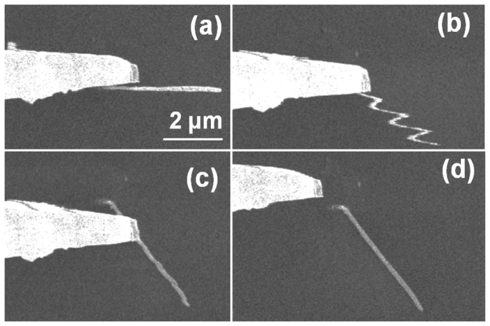
(a) Micromanipulator close to a suspended NW. (b) Manipulator contacting the wire as is moving downwards. The mechanical motion of the probe is transmitted to the NW, resulting in a distorted image, since the motion is faster than the SEM scan. (c) and (d) NW flat on the substrate.
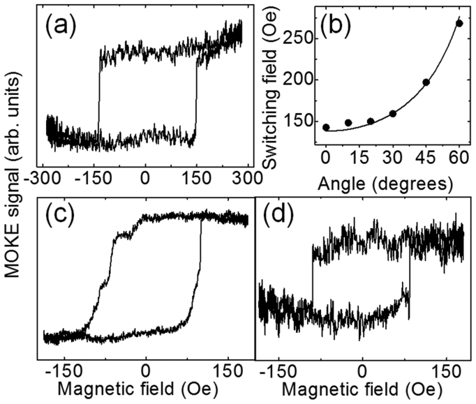
Figure 3(a) shows a MOKE loop for a felled NW when the field is applied along the wire x-axis, showing an abrupt switch of the magnetisation at ~140 Oe. This MOKE configuration for NWs horizontal on a substrate is standard21, with signal changes due to the reversal of the x-component of the magnetisation. The loops measured confirm the single domain state of the wires at remanence, with the magnetisation along the wire axis, due to shape anisotropy. Figure 3(b) shows the switching field of this wire Hsw as a function of the angle θ, formed between the (now in-plane) wire axis and the magnetic field. The data have been fitted to the curling mode of magnetisation reversal for an infinite cylinder:
where a = −1.08(Ø0/Ø)2, Ø is the NW diameter, and Ø0 = 2(A/Ms2)1/2 ≈ 5 λex, with A the exchange stiffness and λex the exchange length. From the fit, we obtain λex = 4 ± 1 nm, in reasonable agreement with values previously reported for Co25,26. The angular dependence observed has been previously found for cylindrical NWs where the main source of magnetic anisotropy is the shape of the wires, and Ø > Ø07, as here. Under those circumstances, the NWs reverse via the curling of a few spins, normally at the edges of the NW, resulting in the nucleation of a small domain, a few hundreds of times smaller than the total volume of the wire, which abruptly expands along it7. A different magnetic behaviour is observed in electrodeposited Co NWs, dictated by a strong magnetocrystalline anisotropy parallel or perpendicular to the wire axis25,27. This is due to the strong texture present in those wires, which is not the case for those studied in this report: TEM analysis (not shown here) reveals 3D-FEBID NWs to be polycrystalline, with ~3–6 nm diameter grains. This microstructure is similar to the one observed in 2D Co nanostripes grown by the same method28, where the magnetic behaviour was found to be dominated by the magnetostatic energy29. We should note that by fitting Hsw(θ) to the curling model we have assumed that the magnetisation reversal is DW nucleation-dominated. If, however, this process were DW propagation-dominated, the Kondorsky model30 should be used. In that case, Hsw (θ) = Hsw(0)/cos(θ), which also gives a satisfactory fit of our data. The similar angular dependence between both models makes it impossible for us to distinguish which of the two mechanisms is present here. In either case, the magnetisation reversal is via the propagation of DWs, and not by coherent rotation of the magnetisation, which would give a different angular dependence for Hsw7,27.
Figure 3. MOKE measurements on in-plane NWs.
(a) and (c) Hysteresis loops of two different wires obtained by averaging 250 individual loops. (d) Single-shot measurement of the same wire as in (c). (b) Dependence of the switching field with the angle formed between the wire axis and the applied magnetic field, fitted to a curling model.
To give a broader picture of the types of hysteresis loops obtained, figure 3(c) shows the MOKE measurement for a NW, where the signal is the result of 250 averages. A multi-step switching behaviour is observed in this case. The significant enhancement of the signal-to-noise ratio for MOKE measurements on felled NWs permits us to perform single-shot measurements (figure 3(d)). The non-averaged loops present single sharp transitions, indicating that the observed broadening of the switching field under averaging is the result of the stochastic nature of the nucleation or propagation processes7,15.
Atomic and magnetic force microscopy
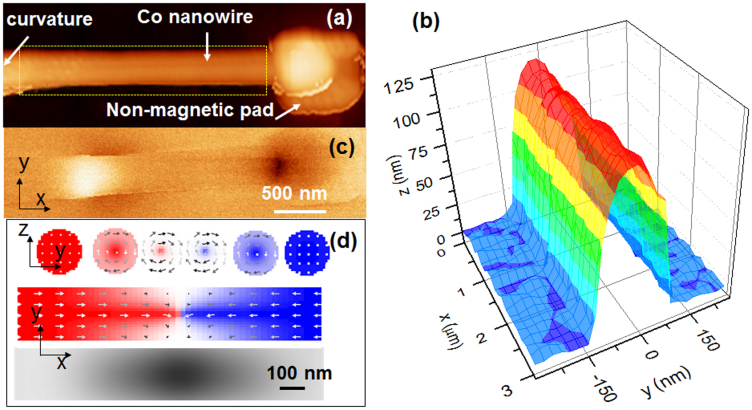
We have performed atomic- (AFM) and magnetic- force (MFM) microscopy measurements on selected felled NWs. Figure 4(a) shows the AFM image of a NW where an additional non-magnetic pad has been deposited by FEBID, using (CH3)3Pt(CpCH3) as gas precursor, to ensure the good adhesion of the NW to the substrate after the felling process. Also, the NW lifts off the substrate at the left side of the image, preventing AFM imaging. Figure 4(b) shows the profile of the NW for the segment marked with a yellow dashed line in figure 4(a). The AFM tip is not able to trace circular sections, overestimating the wire dimension in the y-direction31,32. However, the diameter of the NW can be determined from the maximum height of the wire in the z-direction. In this particular example, Ø = 116 ± 6 nm. In order to achieve such diameter uniformity along several microns, the growth must be performed at the electron-limited regime, but close to the crossover with the precursor-limited regime, to have deposits with a high Co percentage16. Figure 4(c) shows an MFM image of the wire at remanence, after applying a field of ~500 Oe, forming a small angle with the NW axis. Together with the stray field at the right end of the NW, a bright area close to the left edge of the image is observed, corresponding to the presence of a DW. This DW is trapped due to the strong curvature of the NW as it lifts off the substrate. The image confirms the conclusions deduced from MOKE measurements: the mechanism for magnetisation reversal of the wires is the nucleation and propagation of DWs. We have performed micromagnetic simulations33 to study the stability of different types DWs for the Ø/λex ratios present here. We modelled NWs with Ø = 40–100 nm, using parameters for polycrystalline cobalt, modified to take into account the experimental results: Ms = 1190 emu/cm3 (85% of pure Co), A = 1.4 × 10⁻¹¹ J/m (resulting in λex = 4 nm), zero magnetocrystalline anisotropy, cell size = 5 × 4 × 4 nm3. We find that Bloch-point vortex DWs34, as the one shown in figure 4(d), are those with the simplest structure which are stable for these dimensions. The wires are wider than the dimensions for which transverse DWs, which have been predicted to present outstanding dynamic properties35, are energetically favourable. The figure also includes the corresponding MFM image computed from simulations, by calculating the phase shift measured by the microscope, with the tip approximated to be a 40 nm rigid magnetic dipole. See ref. 36 for details. The simulated image shows similar features to the experimental ones. However, additional simulations show small differences between the MFM images corresponding to different types of DWs in cylindrical NWs, much smaller than for flat nanostripes. This, together with the inability of the tip to resolve the real profile of the wire, prevents us from uniquely determining the type of DW observed in these NWs.
Figure 4. Atomic and magnetic-force microscopy of NWs.
(a) AFM image of a felled NW. A non-magnetic pad at the right end of the wire was deposited, and the wire is curved upwards at the left side of the image (b) AFM profile of the NW, corresponding to the yellow dashed area marked in (a). (c) MFM image of the wire showing the presence of a DW (d) Micromagnetic simulations of a NW with Ø = 100 nm hosting a symmetric Bloch-point vortex DW. Top: Different cross sections along the NW axis; middle: top-view of the wire; bottom: MFM image computed from the simulations.
Discussion
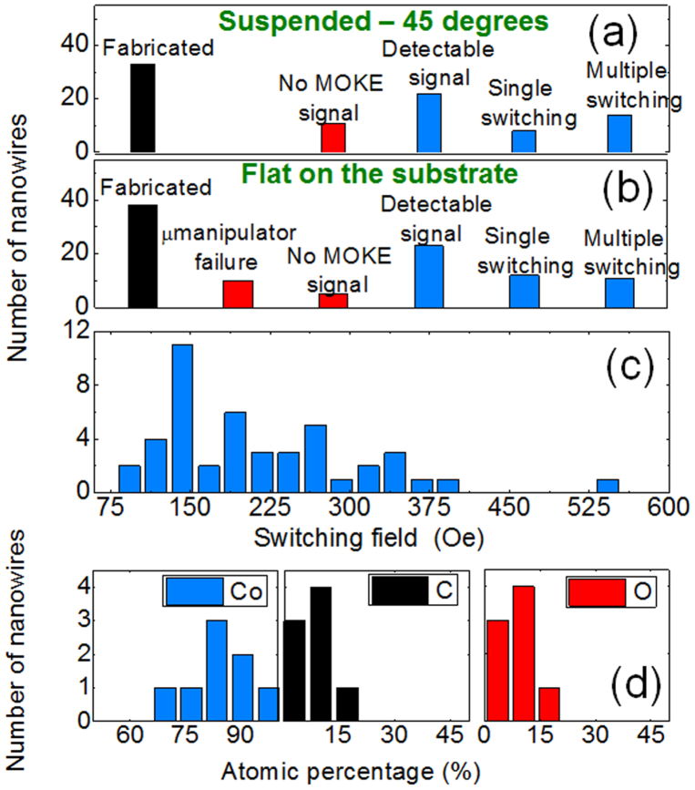
Figure 5 shows a series of histograms which summarise the processes described previously. The histograms compile results for nominally-identical NWs, both suspended and felled, grown in 8 batches, over an 18 month period. In figures 5(a) and (b) we observe that about 60% of the NWs which were grown present a detectable MOKE signal, although this percentage rises up to 80% for successfully felled wires. For those that give a measurable signal, 40–50% present single switching events (± 2 Oe) after 1000 averages.
Figure 5. Statistics of the processes carried out for this work.
(a) and (b) Histograms regarding growth, micromanipulation and magnetic signal of the wires. MOKE data refer to loops with 1000 averages (c) Histogram of the switching fields of the wires. (d) Histograms of the atomic composition of the wires.
Figure 5(c) shows the distribution of switching fields for all the NWs measured, for fields applied along the wire long axis. For suspended NWs, the measurements were performed with the laser spot close to their base, and the switching field observed experimentally has been divided by the denominator of equation (1), with θ = 45°. A significant dispersion of the switching fields is observed, with 75% of the NWs reversing between 110 and 270 Oe. Together with the dispersion in the composition of the wires between batches (see figure 5(d)), the propagation and nucleation fields of DWs along NWs are very sensitive to factors such as defects or geometrical modifications of the wires. Small changes in properties from wire to wire might be responsible for the variation observed here. These data contrast with results for Co 2D micro- and nano-stripes grown by FEBID, which have been shown to have more reproducible switching29. A less uniform deposit is expected in 3D FEBID nanostructures, due to the evolution during growth of factors such as heating, replenishment of gas molecules or beam focusing11,12,20. In spite of an overall large dispersion, the standard deviation of the switching fields for NWs of the same batch was found to be less than 25% for three of the batches, which suggests that future improvements regarding the reproducibility on the growth of 3D NWs are possible.
FEBID, apparently a simple lithography technique, involves tens of parameters, with the composition, morphology or shape of the deposits critically dependent on small variations of the growth conditions11,12. In FEBID each structure is fabricated individually, which is a disadvantage in terms of time, cost and reproducibility with respect to more standard techniques. However, the results shown here demonstrate the unique potential of FEBID to create 3D magnetic nanodevices. By growing NWs in the electron-limited-regime, but close to the precursor-limited-regime, several micron-long, smooth NWs are grown in tens of seconds. The wires have high metallic content, mainly formed by polycrystalline Co. Under external magnetic fields, the magnetisation reverses by the nucleation and propagation of –hundreds of nm wide– DWs. These results represent a significant step towards the use of 3D-NWs for DW-based applications. Together with the development of new strategies to overcome the aforementioned problems, we expect that the use of novel gas precursors and the co-deposition using several gases will make possible the controlled growth of other materials more suitable for spin-transfer torque applications.
In conclusion, we have fabricated and characterised 3D Co nanowires made by FEBID. Under optimised deposition conditions, the nanowires have high aspect-ratio and metallic content, present functional magnetic properties, and can be grown with complex geometries as those required in future 3D nanodevices. Furthermore, we have experimentally shown that the magnetic switching of 3D tilted nanowires can be directly measured by MOKE, offering a means to characterise these 3D magnetic nanostructures.
Methods
Growth parameters, composition and micro-manipulation
The straight NWs were grown by focusing the electron beam on the same point during the full time of exposure. The following conditions were used: base pressure = 5 × 10⁻⁷ mbar, growth pressure = 1–2 × 10⁻⁵ mbar, acceleration voltage = 3 kV, beam current = 21 pA, lateral/vertical distance between the gas injector and beam spot = 50/150 μm. Each NW grows in 1–3 min. The angle formed between the NW axis and the substrate was varied by tilting the stage to the complementary angle, since the wire grows along the electron beam axis. The composition of the deposits, determined by electron-dispersive X-ray spectroscopy, was measured for one wire of each batch. The average composition is (% at): Co = 84 ± 16 %, C = 9 ± 8 % and O = 8 ± 4 %. No significant changes were observed when probing different areas of the NWs. Further details on the growth optimisation will be published elsewhere.
In order to make the NWs fall onto the substrate, a tungsten micromanipulator was used, with tip diameter of ~500 nm. The micromanipulation speed used is 1 μm/s.
Author Contributions
A.F.P. designed the experiments, fabricated, characterised and modelled the wires, and wrote the manuscript. L.S.R. and J.M.D.T. carried out the growth optimisation of the wires. J.L. calculated the MFM images from simulations. All authors discussed the results and contributed to the scientific interpretation as well as to the writing of the manuscript.
Supplementary Material
Supplementary Information-MOKE MEASUREMENTS ON 3D NANOWIRES
Video
Acknowledgments
This research was supported by a Marie Curie Intra European Fellowship project No. 251698: 3DMAGNANOW, a Marie Curie International Outgoing Fellowship project no. 299376: HIGHSPIN and an ERC Advanced Grant project No. 247368: 3SPIN, all funded by the 7th European Community Framework Programme, by the MAT2011-27553-C02 project funded by the Spanish Ministry of Economy (including FEDER funding) and by the I-LINK0026 project funded by the Spanish CSIC. We would like to thank Laura Casado, Rosa Córdoba and Anthony Beguivin for technical help, Agustina Asenjo for discussing MFM results, and Rhodri Mansell for critical reading of the manuscript.
References
- Parkin S. S. P., Hayashi M. & Thomas L. Magnetic domain-wall racetrack memory. Science 320, 190–194 (2008). [DOI] [PubMed] [Google Scholar]
- O'Brien L. et al. Bidirectional magnetic nanowire shift register. Appl. Phys. Lett. 95, 232502 (2009). [Google Scholar]
- Chiba D. et al. Control of Multiple Magnetic Domain Walls by Current in a Co/Ni Nano-Wire. Appl. Phys. Express 3, 073004 (2010). [Google Scholar]
- Kim K.-J. et al. Electric Control of Multiple Domain Walls in Pt/Co/Pt Nanotracks with Perpendicular Magnetic Anisotropy. Appl. Phys. Express 3, 083001 (2010). [Google Scholar]
- Franken J. H. Swagten H. J. M. & Koopmans B. Shift registers based on magnetic domain wall ratchets with perpendicular anisotropy. Nat. Nanotechnol. 7, 499–503 (2012). [DOI] [PubMed] [Google Scholar]
- Cowburn R. P. & Allwood D. U. S. Patent No. 0047156 A1. (1 March 2007).
- Wernsdorfer W. et al. Nucleation of Magnetization Reversal in Individual Nanosized Nickel Wires. Phys. Rev. Lett. 77, 1863 (1996). [DOI] [PubMed] [Google Scholar]
- Ebels U. et al. Spin Accumulation and Domain Wall Magnetoresistance in 35 nm Co Wires. Phys. Rev. Lett. 84, 983–896 (2000). [DOI] [PubMed] [Google Scholar]
- Fusil S. et al. Nanolithography based contacting method for electrical measurements on single template synthesized nanowires. Nanotechnology 16, 2936 (2005). [Google Scholar]
- Piraux L. et al. Template-Grown NiFe/Cu/NiFe Nanowires for Spin Transfer Devices. Nano Lett 7, 2563–2567 (2007). [DOI] [PubMed] [Google Scholar]
- Utke I., Hofmann P. & Melngailis J. Gas-assisted focused electron beam and ion beam processing and fabrication. J. Vac. Sci. Technol. B 26, 1197–1276 (2008). [Google Scholar]
- van Dorp W. F. & Hagen C. W. A critical literature review of focused electron beam induced deposition. Appl. Phys. Rev. 104, 081301 (2008). [Google Scholar]
- Koops H. W. Rapid prototyping and structure generation using three-dimensional nanolithography with electron beam induced chemical reactions. Proceedings of SPIE 5116, 393–401 (2003). [Google Scholar]
- Fernández-Pacheco A. et al. Magnetotransport properties of high-quality cobalt nanowires grown by focused-electron-beam-induced deposition. J. Phys. D: Appl. Phys. 42, 055005 (2009). [Google Scholar]
- Fernández-Pacheco A. et al. Domain wall conduit behavior in cobalt nanowires grown by focused electron beam induced deposition. Appl. Phys. Lett. 94, 192509 (2009). [Google Scholar]
- Serrano-Ramón L. et al. Ultrasmall Functional Ferromagnetic Nanostructures Grown by Focused Electron-Beam-Induced Deposition. ACS Nano 5, 7781 (2011). [DOI] [PubMed] [Google Scholar]
- Nikulina E. Idigoras O. Vavassori P. Chuvilin A. & Berger A. Magneto-optical magnetometry of individual 30 nm cobalt nanowires grown by electron beam induced deposition. Appl. Phys. Lett. 100, 142401 (2012). [Google Scholar]
- Gazzadi G. C., Frabboni S. & Menozzi C. Suspended nanostructures grown by electron beam-induced deposition of Pt and TEOS precursors. Nanotechnology 18, 445709 (2007). [Google Scholar]
- Utke I., Hofmann P., Berger R. & Scandella L. High-resolution magnetic Co supertips grown by a focused electron beam. Appl. Phys. Lett. 80, 4792 (2002). [Google Scholar]
- Utke I. et al. Cross-section Investigations of Compositions and Sub-Structures of Tips Obtained by Focused Electron Beam Induced Deposition. Adv. Eng. Mater. 7, 323–331 (2005). [Google Scholar]
- Allwood D. A., Xiong G., Cooke M. D. & Cowburn R. P. Magneto-optical Kerr effect analysis of magnetic nanostructures. J. Phys. D: Appl. Phys. 36, 2175–2182 (2003). [Google Scholar]
- Qui Z. Q. & Bader S. D. Surface magneto-optic Kerr effect. Rev. Sci. Instrum. 71, 1243–1255 (2000). [Google Scholar]
- Garcia J. A., Saad A. Elbaile L. & Kurlyandska G. V. New Developments in Nanotechnology Research. Editors: Dirote E. V., ed. Nova Science Publishers (2007).
- Leven B. & Dumpich G. Resistance behavior and magnetization reversal analysis of individual Co nanowires. Phys. Rev. B 71, 064411 (2005). [Google Scholar]
- Ferre R. et al. Magnetization processes in nickel and cobalt electrodeposited nanowires. Phys. Rev. B 56, 14066–14075 (1997). [Google Scholar]
- Kläui M. et al. Head-to-head domain-wall phase diagram in mesoscopic ring magnets. Appl. Phys. Lett. 85, 5637 (2004). [Google Scholar]
- Vivas L. G., Escrig J. Trabada D. G., Badini-Confalonieri G. A. & Vázquez M. Magnetic anisotropy in ordered textured Co nanowires. Appl. Phys. Lett. 100, 252405 (2012). [Google Scholar]
- Córdoba et al. Nanoscale chemical and structural study of Co based FEBID structures by STEM-EELS and HRTEM. Nanos. Res. Lett. 6, 592 (2011). [DOI] [PMC free article] [PubMed] [Google Scholar]
- Fernández-Pacheco A. et al. Magnetization reversal in individual cobalt micro- and nanowires grown by focused-electron-beam-induced-deposition. Nanotechnology 20, 475704 (2009). [DOI] [PubMed] [Google Scholar]
- Kondorsky E. On hysteresis in ferromagnetics. J. Phys. (USSR) 2, 161–181 (1940). [Google Scholar]
- Stan G., Ciobanu C. V., Parthangal P. M. & Cook R. F. Diameter-Dependent Radial and Tangential Elastic Moduli of ZnO Nanowires. Nano Lett. 7, 3691 (2007). [Google Scholar]
- Henry Y. et al. Magnetic anisotropy and domain patterns in electrodeposited cobalt nanowires. Eur. Phys. J. B 20, 35–54 (2001). [Google Scholar]
- Micromagnetic simulations were performed using the OOMMF code, available at http://math.nist.gov/oommf/. Accessed in June (2008).
- Wieser R., Nowak U. & Usadel K. D. Domain wall mobility in nanowires: Transverse versus vortex walls. Phys. Rev. B 69, 064401 (2004). [Google Scholar]
- Yan M., Kakay A. Gliga S. & Hertel R. Beating the Walker Limit with Massless Domain Walls in Cylindrical Nanowires. Phys. Rev. Lett. 104, 057201 (2010). [DOI] [PubMed] [Google Scholar]
- Roy P. E. et al. Antivortex domain walls observed in permalloy rings via magnetic force microscopy. Phys. Rev. B 79, 060407(2009). [Google Scholar]
Associated Data
This section collects any data citations, data availability statements, or supplementary materials included in this article.
Supplementary Materials
Supplementary Information-MOKE MEASUREMENTS ON 3D NANOWIRES
Video


