Abstract
Electromigration induced failure development in a copper dual-damascene structure with a through silicon via (TSV) located at the cathode end of the line is studied. The resistance change caused by void growth under the TSV and the interconnect lifetime estimation are modeled based on analytical expressions and also investigated with the help of numerical simulations of fully three-dimensional structures. It is shown that, in addition to the high resistance increase caused by a large void, a small void under the TSV can also lead to a significant resistance increase, particularly in the presence of imperfections at the TSV bottom introduced during the fabrication process. As a consequence, electromigration failure in such structures is likely to have bimodal characteristics. The simulation results have indicated that both modes are important to be considered in order to obtain a more precise description of the interconnect lifetime distribution.
1. Introduction
Three-dimensional (3D) integration has become a very promising technology for the microelectronics industry. Among its main advantages are: high density integration, multifunctionality, better performance, reduced power, heterogeneous integration, etc. [1]. One key component of 3D integration to achieve these features is the through silicon via (TSV) [2]. The TSV consists of a conducting via fabricated trough a silicon substrate, which connects components of different integration levels [1].
Reliability is a critical issue for new emerging technologies, in particular, for TSVs [3]. Electromigration (EM) is one of the main reliability concerns in back-end of line (BEOL) interconnects.
EM failure mechanisms have been extensively studied for copper dual-damascene interconnects, where failure is characterized by the resistance increase with time associated to EM induced material transport. Typically, resistance measurements show an initial period with very small resistance change, followed by a subtle increase phase and further linear growth [4]. Frank et al. [5] have shown that for structures with a TSV formed on a pad at the cathode end of line the resistance development is somewhat different. They have observed that the subtle resistance increase phase does not occur, so that the interconnect resistance remains initially constant and then starts to increase following a logarithmic time dependence. Based on failure analysis methods it was shown that this behavior is due to the growth of a large void under the TSV and concluded that this is the major failure mechanism in such structures.
In this work we investigate the EM failure mechanisms in copper dual-damascene lines with a TSV located at the cathode end of the line. The resistance change of such interconnect structures is studied based on 3D numerical simulations and their lifetimes are modeled. We show that, in addition to the high resistance increase caused by a large void, a small void under the TSV can also lead a significant resistance increase, mainly due to imperfections at the TSV bottom introduced during the fabrication process. Comparison with the available experimental results indicates that both modes have to be considered for a more precise description of the interconnect lifetime distribution.
2. Modeling
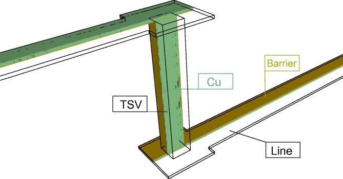
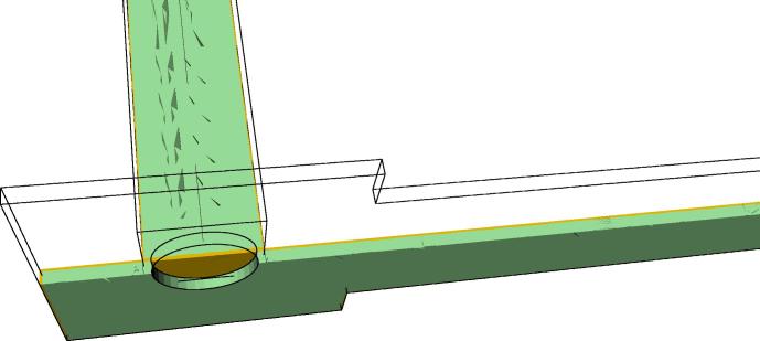
In [5] EM experiments using downstream electron flow showed void formation and growth under the TSV at the cathode end of a line as sketched in Figs. 1 and 2. It was observed that the development of the resistance as a function of time can be divided in two periods: at first the resistance remains practically constant, which is then followed by a measurable resistance increase. Failure analysis indicated that during the first period the void diameter is smaller than the TSV section, while the measurable resistance increase period starts as soon as the void diameter becomes larger than the TSV section. We analyze both periods in more detail in the following sections.
Fig. 1.
Copper dual-damascene line/TSV structure.
Fig. 2.
Detail of the TSV bottom and void under the via.
2.1. Resistance change as a function of void size
Considering a cylindrical void with radius r under the TSV, as shown in Fig. 2, the infinitesimal resistance change for r ⩾ rTSV is given by [5]
| (1) |
since the void causes electrons to flow through the barrier layer along a length dr and conducting area 2πtbr. Here, ρb is the barrier resistivity and tb is the barrier layer thickness at the bottom of the via. Thus, the resistance increase in relation to R(rTSV) is given by
| (2) |
where rvoid and rTSV are the void and the TSV radii, respectively.
Frank et al. [5] observed a very small resistance change while rvoid ⩽ rTSV, so a negligible resistance change was assumed for this period of void growth. Thus, applying R(rTSV) = R0 in Eq. (2), where R0 is the initial resistance, the total resistance change can be written as
| (3) |
Eq. (3) is applicable as long as the resistance change is sufficiently small for the range rvoid ⩽ rTSV, so that the approximation R(rTSV) = R0 can be used. This assumption cannot be always fulfilled, therefore, using Eq. (2), the total resistance change is given by
| (4) |
For rvoid < rTSV, the resistance change is caused by the reduction of the effective conducting area at the TSV bottom. In absence of voiding, the conduction area through the barrier layer is equal to the cross sectional area of the TSV, . In the presence of a void, the effective conduction area becomes . Thus, the resistance increase is written as
| (5) |
This equation suggests a rapid resistance increase as the void radius approaches the TSV one. However, it has a singularity at rvoid = rTSV, which prevents the calculation of ΔR(rTSV) and also leads to a discontinuity between Eqs. (4) and (5). This is a drawback of the model. Nevertheless, later it will be shown that it satisfactorily describes the resistance change development for a wide range of rvoid, namely, rvoid ⩽ 0.95 rTSV. Therefore, the discontinuity does not affect the analysis significantly and, moreover, the modeling is supported by numerical simulation results, from where ΔR(rTSV) can be extracted.
It should be pointed out that the rapid resistance change predicted by Eq. (5) suggests that it is possible that the resistance increase for failure ΔRc is reached for a smaller critical void. Since a smaller void implies a shorter time to build it, earlier failures than those estimated from Eq. (4) are expected to occur.
The models derived above assume a circular TSV, while the via used in the experimental test structure described in [5] and used in this work is approximately square. Therefore, rTSV should be viewed as an effective via radius. This does not affect the modeling and later we will show that rTSV can be determined by fitting Eqs. (4) and (5) to the curves of resistance change as a function of void radius obtained from numerical simulations.
2.2. Resistance change with time
In order to model the resistance variation with time during EM stress the void growth rate rvoid(t) has to be calculated. Once rvoid(t) is known, ΔR(t) is determined by substitution in Eq. (4) or Eq. (5) for large or small voids, respectively. In this way the interconnect TTF can be estimated for a given resistance change ΔRc used as failure criterion.
During EM stress several driving forces for vacancy migration are acting at the same time, so the total vacancy flux is given by [6]
| (6) |
where Dv is the effective vacancy diffusivity, Cv is the vacancy concentration, eZ∗ is the effective charge, ρ is the electrical resistivity of the metal, is the current density, Q∗ is the heat of transport, f is the vacancy relaxation ratio, Ω is the atomic volume, σ is the hydrostatic stress, k is the Boltzmann’s constant, and T is the temperature. The second term on the right-hand side describes the electromigration flux, while the other terms represent components of a back-flux [7–9]. It is commonly assumed that if the product jL is much larger than the critical Blech’s product (jL)c, the back-flux can be neglected [10]. Thus, Eq. (6) is simplified to
| (7) |
Void growth is governed by the rate of vacancies captured by the void. Assuming a constant vacancy flux along the line, the volume formed by capturing vacancies up to a time t is given by [5]
| (8) |
where α (0 < α < 1) is the ratio of vacancies captured by the void, Ωv = fΩ is the vacancy volume, and Al is the line cross sectional area. Considering a cylindrical void under the TSV [5] we can write
| (9) |
and substituting Eq. (7) yields a void radius growth as a function of time
| (10) |
where h is the line thickness. This equation has been obtained following the observations presented by Frank et al. [5]. A more detailed derivation is beyond the scope of this work and can be found in the aforementioned reference.
Substituting rvoid(t) given by Eq. (10) into Eq. (4) yields
| (11) |
where t0 is given by
| (12) |
t0 defines the time at which the void radius becomes equal to the radius of the TSV (rvoid = rTSV), so that the logarithmic resistance increase described in Eq. (11) starts. Thus, Eq. (11) is valid as long as rvoid ⩾ rTSV, which corresponds to the period of void growth when t ⩾ t0. As in the previous section, if the approximation R(rTSV) = R0 is used, Eq. (11) reduces to [5]
| (13) |
In turn, substitution of Eq. (10) into Eq. (5) leads to
| (14) |
which is valid as long as the void remains smaller than the via (rvoid ⩽ 0.95 rTSV).
2.3. TTF estimation
Eqs. (11) and (14) describe the resistance change for large and small voids, respectively. If the maximum allowed resistance change ΔRc is reached for a sufficiently large void (rvoid > rTSV), the interconnect TTF is determined by Eq. (11). In turn, if a small void (rvoid ⩽ 0.95 rTSV) can produce a significant resistance increase, the failure time is governed by Eq. (14). Therefore, for a certain ΔRc the lifetime of structures as those shown in Fig. 1 can be estimated from
| (15) |
with , and from
| (16) |
Although Frank et al. [5] have assumed that EM failures in these structures follow solely Eq. (15), the modeling proposed above indicates that another failure mode, governed by Eq. (16), is likely to exist. In addition, this new failure mode is related to smaller voids and, thus, to shorter lifetimes. Therefore, it corresponds to an early failure mode, which is critical for a correct assessment of the reliability of these interconnect structures.
3. Results and discussion
The resistance change caused by the growth of a void located under the TSV was determined from numerical simulations. A detailed view of the structure and void at the TSV bottom are shown in Figs. 1 and 2. The dimensions, material parameters, and simulation conditions are shown in Table 1.
Table 1.
Parameters used in calculations [5].
| Parameter | Value |
|---|---|
| w | 4.0 μm |
| h | 0.25 μm |
| Al | 1.0 μm2 |
| rTSV | 1.4 μm |
| tb | 70 nm |
| α | 1.0 |
| f | 0.4a |
| Ω | 1.182 × 10⁻²³ cm3a |
| Dv | 1.0 × 10⁻⁴ cm2/s |
| Cv | 1.0 × 1016 cm−3 |
| Z∗ | 1.0 |
| ρ | 2.5 × 10⁻⁸ Ω m |
| ρb | 800 μΩ cm |
| R(rTSV) | 21.44 Ωb |
| R0 | 20.41 Ωb |
| ΔRc | 2.0 Ω |
| j | 2.5 MA/cm2 |
| T | 300 °C |
| e | 1.6 × 10⁻¹⁹ C |
| k | 1.38 × 10⁻²³ J/K |
Sarychev et al. [6].
Numerical simulations.
Following the observations of Frank et al. [5], a cylindrical void is placed under the via and its radius is gradually incremented following Eq. (10). For each void size the resistance of the interconnect is determined from the numerical solution of the Laplace equation. In this way we are able to extract the resistance change of the interconnect shown in Fig. 1 for the whole period of void growth.
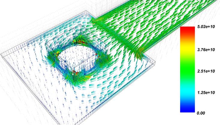
Fig. 3 shows the electron current density distribution at the TSV bottom in the presence of a void. The void causes a reduction of the effective conducting area at the TSV bottom. The electron flow is displaced towards the corners of the via, which leads to current crowding in this region, as can be readily seen in Fig. 3. This supports the modeling approach described in Section 2.1.
Fig. 3.
Electron current density distribution (in A/m2) under the TSV in the presence of a void. Current crowding towards the corners of the via can be seen.
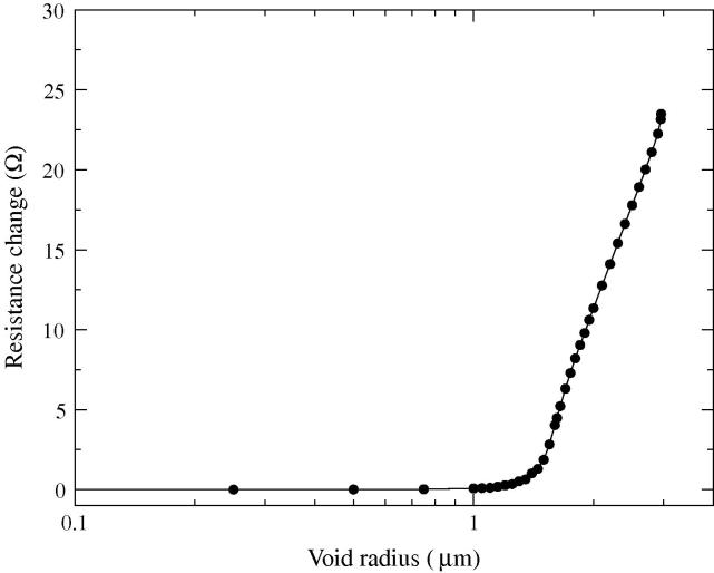
The resistance change as a function of void radius is shown in Fig. 4. Two phases of resistance development can be seen. The resistance change is practically negligible for small void radii (rvoid < rTSV = 1.4 μm). For larger voids, however, a significant resistance increase is observed. Note that the void radius axis is plotted in logarithmic scale and that the resistance appears to closely follow a linear increase in this scale. These results suggest that the approximation R(rTSV) = R0 can be applied, so that the resistance change is well described by Eq. (3). Nevertheless, in order to further investigate the resistance change behavior shown in Fig. 4, a more detailed analysis is presented below for each phase of resistance development.
Fig. 4.
Numerical simulation of resistance change as a function of void size under the TSV.
3.1. Resistance change for large voids
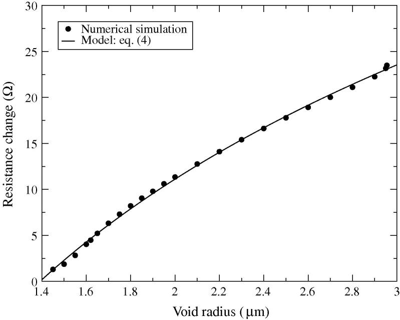
The resistance change of the interconnect line as a function of the void radius within the range rvoid > 1.4 μm is shown in Fig. 5. The symbols represent numerical simulation results obtained for different void sizes. The solid line is a fit to the simulated data according to the model given in Eq. (4). The model correctly describes the resistance change for the tested void radius range. Furthermore, the numerical simulation results reproduce the logarithmic resistance increase suggested by Frank et al. [5]. By fitting Eq. (4) with the numerical simulation results we have obtained as effective TSV radius rTSV = 1.44 μm.
Fig. 5.
Interconnect resistance change as a function of void radius for rvoid > rTSV.
3.2. Resistance change for small voids
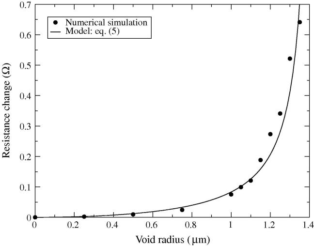
The simulated resistance change as a function of void size for rvoid < 1.4 μm is shown in Fig. 6. Although the magnitude of the resistance change is small, a rapid increase is expected as the void grows. A very good agreement between the numerical simulations and the analytical model given by Eq. (5) is obtained for the range rvoid ⩽ 0.95 rTSV. The estimated effective TSV radius is rTSV = 1.43 μm, which is very close to the value previously determined for the large void case.
Fig. 6.
Resistance change as a function of void radius for small voids (rvoid ⩽ 0.95 rTSV).
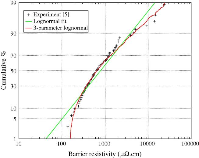
Since the resistance increase for rvoid < rTSV is rather small, EM failures are, in principle, expected to occur for critical void radii in the range rvoid > rTSV [5]. In this case the interconnect lifetime is obtained from Eq. (15). However, imperfections on the bottom of the TSV are typically introduced during the fabrication process [11]. In particular, control of the thin barrier layers at the bottom of the TSV is a key issue and has a significant impact on the structure reliability. As a consequence of these imperfections, Frank et al. [5] observed a high variation of the barrier layer resistivity (100–20000 μΩ cm) estimated from the experimental results. This is shown in Fig. 7, where the symbols represent experimental data and the lines are fits using a standard lognormal distribution and 3-parameter lognormal distribution [12]. Note that the 3-parameter lognormal distribution provides a very good fit to the data. The extracted minimum barrier resistivity is about 115 μΩ cm, which is close to the expected value 200 μΩ cm. This barrier resistivity distribution should be regarded as an effective parameter which takes into account mainly the dispersion of the barrier layer thickness of the TSV bottom.
Fig. 7.
Barrier resistivity distribution. The symbols represent the experimental data extracted by Frank et al. [5] and the lines show possible fits of the distribution.
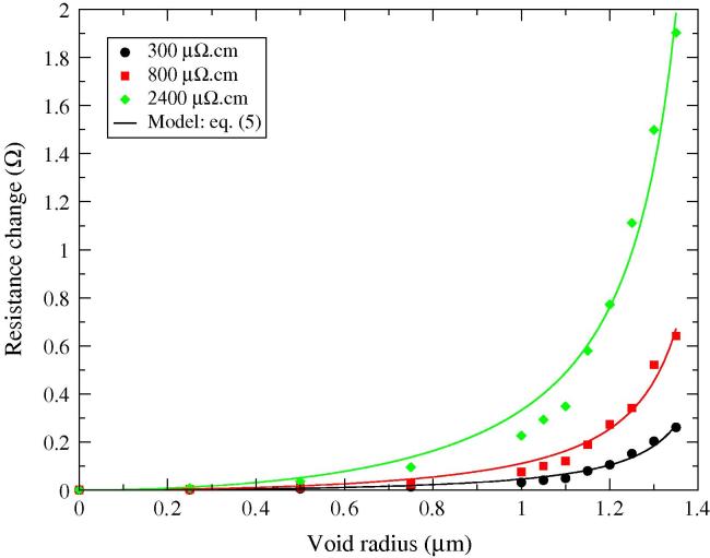
The impact of such variations on the resistance change due to a small void under the TSV for different values of barrier resistivity is shown in Fig. 8. The variation of the effective barrier resistivity affects the structure resistance significantly, leading to a large resistance increase, even when the void size is still smaller than the via section. Taking a 10% resistance increase as failure criterion, we estimate that for ρb ≳ 3000 μΩ cm the interconnect failure is triggered also for voids which rvoid < rTSV. It should be pointed out that these failures form an additional failure mode. Furthermore, since a shorter time is needed to grow a smaller void, this failure mechanism constitutes an early failure mode.
Fig. 8.
Resistance change due to a small void under the TSV for different values of barrier resistivity.
According to the data published in [5], such a high barrier resistivity is found at a cumulative percentile of about 90%. This means that early failures would only be “visible” in lifetime distribution curves for low cumulative percentiles, in particular less than 10%. Considering that the reliability assessment of an interconnect is typically performed at very low failure percentiles, the early failures described above might be the main relevant mechanism for EM failure in copper dual-damascene line/TSV structures.
3.3. TTF estimation
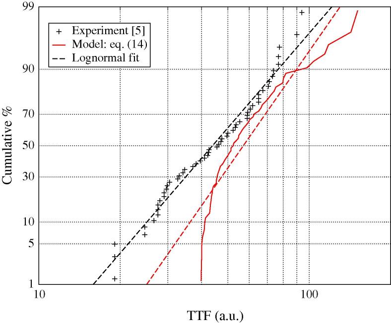
Applying the 3-parameter lognormal fit of the barrier resistivity shown in Fig. 7 into Eq. (15), in addition to the parameters listed in Table 1, we obtain a theoretical TTF distribution. The results are shown in Fig. 9 together with the experimental data. Lognormal fits are also shown as reference. The theoretical results have been determined considering the large void mode only and we can see that they don’t precisely describe the experimental TTF distribution. This is particularly critical for shorter lifetimes (smaller failure percentiles), while for longer lifetimes the theoretical and experimental results are somewhat closer.
Fig. 9.
TTF distribution obtained considering the large void failure mode only (Eq. (15)).
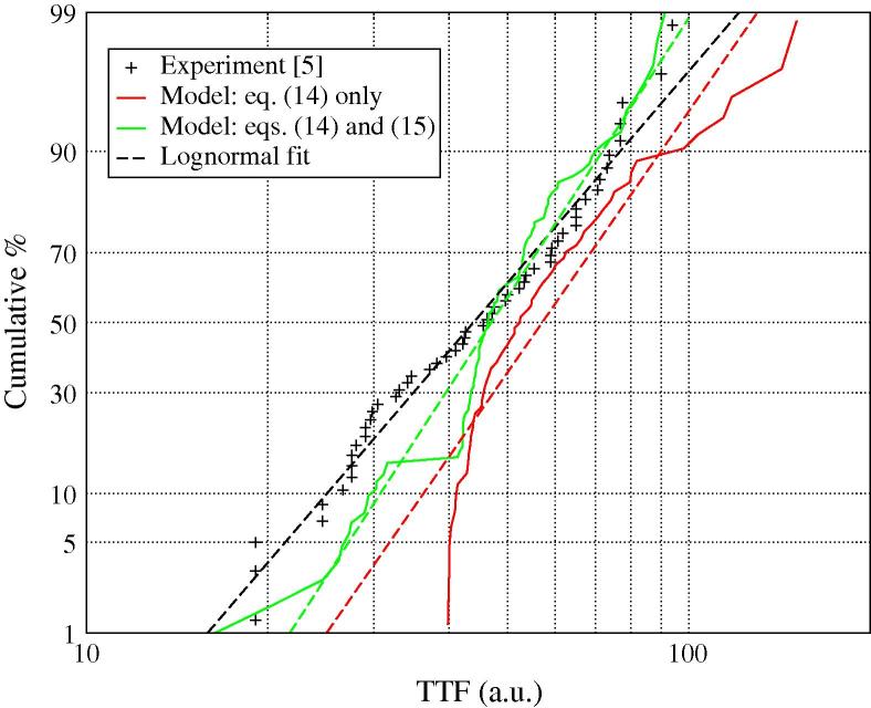
Previously, we have shown that there exists an additional failure mode which is expected to occur at smaller failure percentiles. Taking this extrinsic mode also into account, the TTF distribution given in Fig. 10 has been obtained. The TTF calculations based on the large void mode are also shown for comparison. Considering this additional mode yields in general a better approximation to the experimental results, mainly for shorter lifetimes at lower percentiles. An important issue to consider is the percentile for which the change of late to early mode takes place. In our calculations this percentile is determined by the used barrier resistivity distribution and lies about 13%. Thus, below this value failures are due to the small void mode, while the remaining failures above that percentile are due to the large void mode. Note that around the point of mode change a larger error between the experiment and the simulations is observed. Since more detailed experimental data at such lower percentiles are not available, a more precise estimation of the actual ratio of early/late failures is not possible.
Fig. 10.
TTF distribution obtained considering both failure modes, described by Eq. (15) and by Eq. (16).
4. Conclusion
It was shown that small voids under the via of a copper dual-damascene line/TSV structure generated by EM material transport can cause a significant interconnect resistance increase, particularly in the presence of imperfections on the TSV bottom produced during the fabrication steps. We have proposed a model which satisfactorily describes such resistance increase. In addition, we verified that upon triggering the line failure, this mechanism forms an extrinsic, early failure mode, which acts primarily at low cumulative percentiles, and is expected to have a significant impact on the interconnect reliability assessment. Comparison of the simulation results with experimental data has indicated that both modes are important to be considered for a better description of the TTF distribution.
Acknowledgments
The authors would like to thank T. Frank for helpful discussions. This work was supported by the Austrian Science Fund FWF, project P23296-N13, and also by the European Union Project COCOA.
References
- 1.Lu J.-Q., Rose K., Vitkavage S. 3D integration: why, what, who, when? Future Fab Intl. 2007;23:25–27. [Google Scholar]
- 2.Motoyoshi M. Through-silicon via (TSV) Proc IEEE. 2009;97:43–48. [Google Scholar]
- 3.Koyanagi M. 3D integration technology and reliability. In: Proceedings of the International Reliability Physics of Symposium; 2011. p. 328–4.
- 4.Doyen L., Petitprez E., Waltz P., Federspiel X., Arnaud L., Wouters Y. Extensive analysis of resistance evolution due to electromigration induced degradation. J Appl Phys. 2008;104:123521. [Google Scholar]
- 5.Frank T, Chappaz C, Leduc P, Arnaud L, Lorut F, Moreau S, et al. Resistance increase due to electromigration induced depletion under TSV. In: Proceedings of the International Reliability Physics of Symposium; 2011. p. 347–52.
- 6.Sarychev M.E., Zhitnikov Y.V., Borucki L., Liu C.-L., Makhviladze T.M. General model for mechanical stress evolution during electromigration. J Appl Phys. 1999;86(6):3068–3075. [Google Scholar]
- 7.Blech I.A. Electromigration in thin aluminum films on titanium nitride. J Appl Phys. 1976;47(4):1203–1208. [Google Scholar]
- 8.Blech I.A., Herring C. Stress generation by electromigration. Appl Phys Lett. 1976;29(3):131–133. [Google Scholar]
- 9.Blech I.A., Tai K.L. Measurement of stress gradients generated by electromigration. Appl Phys Lett. 1977;30(8):387–389. [Google Scholar]
- 10.Oates A.S., Lin M.H. Electromigration failure distribution of Cu/low-k dual-damascene vias: impact of the critical current density and a new reliability extrapolation methodology. IEEE Trans Device Mater Reliab. 2009;9(2):244–254. [Google Scholar]
- 11.Frank T, Chappaz C, Leduc P, Arnaud L, Moreau S, Thuaire A, et al. Reliability approach of high density through silicon via (TSV). In: Proc IEEE electronics packaging technology conference (EPTC); 2010. p. 321–4.
- 12.Li B, Christiansen C, Gill J, Filippi R, Sullivan T, Yashchin E. Minimum void size and 3-parameter lognormal distribution for EM failures in Cu interconnects. In: Proceedings of the International Reliability Physics of Symposium; 2006. p. 115–22.


