Abstract
Picoliter droplets actuated on an electrowetting-on-dielectric (EWD) actuator are demonstrated. In this study, the physical scaling of electrodes for 33 μm and 21 μm EWD devices resulted in droplets of 12 pl and 5 pl being dispensed respectively in conjunction with 3 μm SU8 gaskets. The stacked multi-layer insulators in the actuators consisted of 200 nm tantalum pentoxide (Ta2O5) and 200 nm parylene C films deposited and coated with 70 nm of CYTOP. The voltages for dispensing droplets on chips without any external pressure sources are 17.1 Vrms and 22 Vrms for these two sets of devices. A 12 pl droplet can be split into two 6 pl daughter droplets at 18.7 Vrms with 33 μm electrode devices. Droplet manipulation is also demonstrated with paramagnetic beads and buffer solutions with proteins. In addition, electrodes with interlocking protrusions and special featured reservoir gasket are designed to facilitate droplet dispensing on these scaled EWD devices. In order to improve sealing of the two-piece sandwich EWD structure, a soft material, Norland Optical Adhesive (NOA), was coated on the top plate along with pressure on top. We demonstrate that based on fundamental theories and experiments, the dimensional scaling of EWD devices has not yet met a limitation as long as the EWD device can be sealed well.
Keywords: Picoliter droplet, Digital microfluidics, Electrowetting on dielectric, Multi-layer insulator
1. Introduction
In recent years, digital microfluidic manipulation of droplets has been widely investigated as a platform for the transport of chemical or biomedical liquids on biochips [1]. The ultimate goals are to reduce the laboratory reactants and procedures and miniaturize the instruments. With high throughput and minimized reagent consumption, droplet-based systems can provide benefits to the applications of medical diagnosis, drug delivery, point of care, environmental monitoring, and basic scientific research with speed, convenience, low-cost, and reliability.
An EWD device is a liquid droplet actuator based on controlling charges at the interface of a liquid and an insulator over buried electrodes [1–3]. The droplets of microliter or nanoliter sizes can be promptly driven to a precise position, which is not achievable by any other microfluidic methods [4]. EWD actuators have been shown to transport, split, mix, and dispense droplets from on-chip reservoirs. Such liquid control gives more flexibility and better choices for multiple applications performed on a common platform [5–10]. This technique has been adapted to applications, such as polymerase chain reaction (PCR) [11,12], clinical diagnostics [13], proteomic sample preparation [14], DNA ligation [15], simple separations [16], DNA sequencing [17,18] and other complex biochemical [19,20] or biophysical [21] techniques. For most biomedical or biochemical research, reagents and chemical samples are among the most expensive items used in experiments, as compared to machines and upstream costs. Miniaturized devices with picoliter droplets promise to provide the benefits of high throughput, fast diagnosis, but with lower volumes of reagent required.
The electrode sizes used in previous studies were in the range of 750–1500 μm, and the droplet volumes were nano-to-microliter scale [3,6,7,9,22]. We previously reported a multi-layer insulator EWD device, consisting of tantalum pentoxide (Ta2O5) and parylene C, and the smallest volume of 30 pl droplets could be dispensed with 35 μm electrodes at 30 V [10]. Nelson and Kim [23] also fabricated monolithic EWD chips to actuate 100 pl droplets at 30 Vrms. Here, we experimentally demonstrate further scaled, low voltage, picoliter EWD devices. To allow for low-voltage operation, multilayer insulators were still implemented. In addition, the interleaved electrode design and the special gasket neck opening design facilitate droplet dispensing on these scaled EWD actuators. A soft material layer of Norland Optical Adhesive (NOA) is coated on the top plate to perform better sealing. The physical scaling of electrodes is designed and demonstrated for 33 μm and 21 μm electrodes to dispense droplets of 12 pl and 5 pl respectively with 3 μm gaskets at 17.1 Vrms and 22 Vrms on chip without any external pressure sources. A 12 pl droplet can be dispensed and split into two 6 pl daughter droplets on 33 μm electrodes at the voltage as low as 18.7 Vrms. Not only deionized (DI) water is demonstrated, but also droplets of buffer solution containing paramagnetic beads and with some concentration of proteins have been manipulated on scaled devices.
2. Electrowetting theory
Electrowetting is a principle extended from electrocapillarity, where an electric field changes the effective surface energy between a solid electrode and a liquid interface to induce a driving force [3,24]. The mathematical model of electrowetting on dielectric that relates the applied voltage, V, and the droplet contact angle change is given by the Lippmann–Young equation [25]:
| (1) |
where θ and θ0 are the contact angles with and without applying voltage, γSL is the interfacial tension between the droplet and filler medium, εr is the relative dielectric constant of the insulator layer, ε0 is the permittivity of vacuum, and t is the thickness of the insulator. The droplet wets the electrode surface as the contact angle decreases and the surface becomes effectively less hydrophobic along the contact line while voltage is increased. The variation of contact angle or wettability shift is caused predominantly by the charge-induced change in the solid-liquid interfacial tension [3].
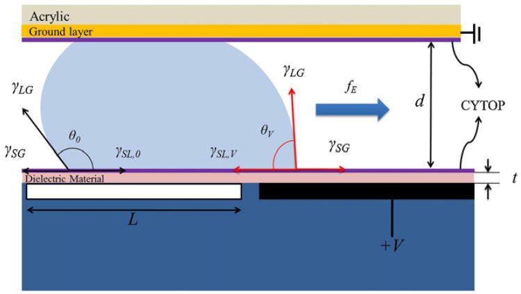
Since the voltage applied changes the contact angle of the droplet and the interfacial tension between the electrode and droplet, an actuator using EWD is proposed using this characteristic to manipulate droplets in micro-channels [3,5,6], as shown in Fig. 1. When a voltage is applied on an adjacent electrode, the solid–liquid interfacial tension (γSL) difference between active and non-active electrodes induces a wetting force (fE) to distort the droplet and even to move the droplet forward if the force exceeds the drag forces and contact-line friction. Electrowetting actuators require a droplet to overlap the adjacent electrode when the droplet rests on the biased electrode, so that the droplet can response to the voltage applied on the adjacent electrode. Therefore, the interleaves electrodes were designed to facilitate the droplet actuation. Even if the droplet is slightly smaller than the electrode, the droplet can still overlap the protrusions of adjacent electrodes and be wetted when a voltage is applied.
Fig. 1.
The side view of a EWD actuator with an applied voltage on the adjacent electrode. The difference of γSL between two ends of the droplet induces the electrowetting force fE.
According to our previous research results [2,10], the determining factors for low voltage EWD are the thickness and dielectric constant of the insulator, and the fluid choices of droplets and filler medium. Regardless of the insulator effects, the threshold voltage ratio for actuation in air to actuation in oil is 1.9–2.5 [2]. Thus, all the EWD devices in this study were operated in a 1.5 cSt silicone oil medium (γSL = 47 mN/m) to have lower actuation voltages and also prevent liquid vaporization. The other factor affecting the actuation voltage is the thickness-to-dielectric-constant ratio of the insulator layer. We demonstrated that multi-layer insulator EWD devices, consisting of stacked insulators of tantalum pentoxide (Ta2O5, εr ∼ 23) and parylene C (εr ∼ 3) thin films, could provide adequate EWD operating voltage ranges that avoid insulator breakdown and allow for reliable operation [10].The stacked of insulators in this study were 200 nm Ta2O5 and 200 nm parylene C.
3. Device design and fabrication
3.1. Device design
The electrode sizes and configurations are very important parameters in the physical dimensional scaling of EWD devices, because the electrowetting force is directly proportional to the area and contact line of the droplet that overlaps the adjacent electrode. Another key element is the gasket height and channel structure design in the actuator, because the gasket thickness determines the liquid volume per area driven by the electrowetting force and affects the capability of liquid manipulation. The compatible design of electrodes and gaskets provides the best platform for droplet manipulations on chip. The smallest electrode sizes ever reported for electrowetting based devices were 100 μm and 35 μm with 20 μm SU8 gaskets for 300 pl and 30 pl droplets manipulation respectively [10].
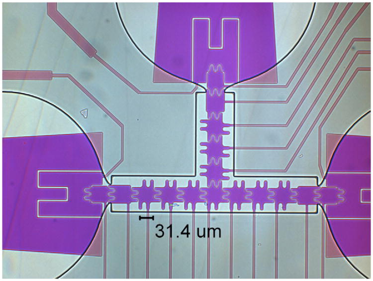
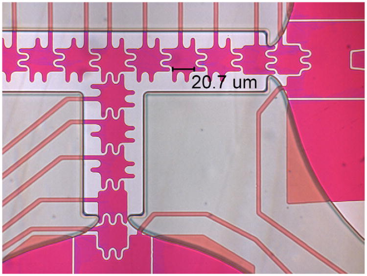
Two different sizes of electrodes were designed to demonstrate scaling. Dimensional-scaled electrodes were designed having sizes (L) of 33 μm with an 18 μm base and 6 μm round interlocking shapes, and L = 21 μm with a 10 μm base and 3 μm interlocking protrusions. Spaces between electrodes of 3 μm were used due to the photo mask limitation of 3 μm features, as shown in Figs. 2 and 3. In order to provide more force and improve the droplet dispensing from the reservoirs, the reservoir electrode was designed with a trapezoidal shape with wide margins toward the neck, which provided larger wetting area, so that when this reservoir electrode was turned on, the liquid would flow forward. Interlocking fingers facilitated the droplet electrowetting, since the droplet would overlap the adjacent electrodes while resting on one biased electrode [26]. The larger overlapping area allows for a significantly larger electrowetting force when an adjacent electrode is activated.
Fig. 2.
33 μm electrode design with rounded interlocking fingers of 18 μm long, 6 μm wide, and 3 μm spaces between electrodes.
Fig. 3.
21 μm electrode design is similar to the 33 μm electrode device, with fingers of 10 μm long and 3 μm wide, and the spaces between electrodes are 3 μm.
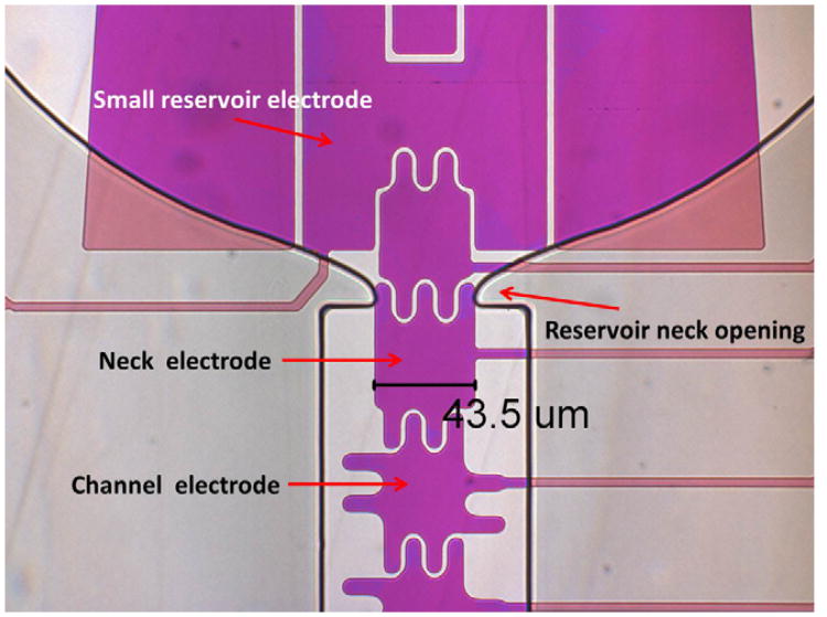
In addition, a small reservoir electrode was put in the front of each reservoir to keep liquid close to the neck opening while turned on, as shown in Fig. 4. The neck electrode was slightly larger than the channel electrodes with three fingers on the opening side, allowing for a larger overlapping area, which resulted in a greater electrowetting force. Based on the previous experience of dispensing droplets on EWD devices, the reservoir neck opening helped to focus the extracted liquid finger and to assist pinch off of the liquid at the neck during liquid dispensing from a reservoir. However, a thick reservoir neck opening increased the difficulty of pulling out liquid. Thus, the gasket design at the reservoir neck opening was tapered to a point on either side to facilitate pulling liquid out of reservoirs and pinching off liquid, as shown in Fig. 4.
Fig. 4.
Special neck opening designs for 33 μm electrode devices. The body of the neck electrode is slightly largerthan that of channel electrodes and three fingers at the opening side with the tapered gasket opening can facilitate pulling out liquid from the reservoir.
3.2. Device fabrication
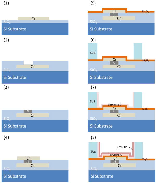
Two-level metal EWD devices were fabricated on 2 cm × 3 cm silicon wafer pieces coated with 150 nm of SiO2 as a bulk insulation layer. With a two-level-metal process interconnects are routed on the lower level, which is insulated from the top level electrodes by a 1 μm silicon dioxide film. By burying the interconnecting wires beneath the electrodes, electrowetting is restricted to only the electrode, and the footprint of the device can be made more compact while allowing more flexibility in the electrode layout. The steps in the two-level metal EWD device process are listed below, and shown in Fig. 5:
The first layer of 70 nm Cr for the electrode connections was deposited by E-beam evaporation and patterned by Cr etchant with approximately 3 μm positive photoresist S-1813.
1 μm layer of PECVD SiO2 was deposited as an inter-layer insulator.
Via holes were next etched in a buffered oxide etchant (BOE, 10 parts 40% NH4F and 1 part 49% HF) for 700 s, and filled with patterned sputtered aluminum.
The second layer of 70 nm Cr for the electrodes and pads was again deposited and patterned (same as process 1).
200 nm Ta2O5 were sputtered as the first layer dielectric layer of EWD by an RF dielectric sputtering system (Kurt Lesker PVD 75) with a 99.99% Ta2O5 target. The deposition power was set at 200 W and the deposition pressure was set at 15 mTorr with 10% oxygen percentages in the chamber.
An SU-8 gasket was spun on the wafer, and developed. The SU-8 gasket thickness (d) was dependant to the electrode size and determined by the desired d/L ratio of approximately 0.1–0.2 [2,3,8]. For the devices with L = 33 μm and 21 μm, the gaskets thicknesses formed were 7 μm, 5 μm, and 3 μm.
A 200 nm second dielectric layer of parylene C was deposited in the parylene coater.
Finally, the hydrophobic layer, composed of 70 nm CYTOP, was spun on the wafers at 3000 rpm, then the film was annealed on a hot plate at 110°C for 1 min, and the devices were placed in a vacuum desiccator over night.
Fig. 5.
The fabrication process for EWD actuators.
For one-level-metal devices, the process starts from step 4 of the two-level metal process, which avoids three photolithography steps, and allows the whole fabrication to be finished in two to three work days. When the electrode number is fewer than the control pads, which means each electrode can be independently controlled without complex bussing, this one-level-metal structure is a better choice to have devices tested in a shorter fabrication time.
The other fabricated part of a EWD device is the top plate, which is a 3 cm × 5 cm acrylic (polycarbonate) piece that covers the entire device with additional space for the ground pad connection. Holes (approximately 500 μm in diameter) were drilled at the locations of the reservoir injection ports to dispense liquid into the reservoirs. For larger scale (100 μm and 35 μm electrodes) devices, the top plate was a piece of polycarbonate with sequential depositions of ITO and CYTOP serving as a ground layer and a hydrophobic layer respectively [10]. Since the gasket height was lower than 10 μm and the structure of the device was smaller, the surface topography tolerance and the fabrication accuracy for SU8 decreased. The problem first faced was that of sealing the channel, especially the edges of the channel and the neck of the reservoir opening. The channel and reservoir volumes became much smaller, so while loading liquid onto the device, the pressure from the manually controlled pipette would squeeze the liquid out of the reservoir. Thus, the liquid would no longer be confined in the reservoir by the gasket. Due to the pressure sealing method, a layer of elastic material on the top plate might be able to diminish the sealing issue caused by the surface roughness and fabrication inaccuracy. For an elastic and soft material, polydimethylsiloxane (PDMS) is the most common choice for microfluidic applications, but PDMS would absorb silicone oil, which was the filler medium for EWD devices in this study. Instead, Norland Optical Adhesive (NOA, ThorLabs) was spin-coated on the top plate with 2500 rpm for 60s to get an approximately 50 μm thick film. The conductive polymer polydioctyl-bithiophene (PDOT, Aldrich) was then spin-coated for 150 nm as the ground layer followed by the hydrophobic layer of CYTOP. With pressure on the top plate, the NOA layer could compensate the roughness of the SU8 surface at the edges and channel necks, and seal the channel on the 7 μm and 5 μm gasket. However, for the gasket of 3 μm thickness, the end point of the channel neck could not be accurately fabricated due to the limitation of photolithography, especially for 21 μm electrodes. The neck edge was not sharply defined, so that when liquid was pulled out of the reservoir into the channel, the liquid flowed over the neck, which reduced the pinch-off during dispensing.
4. Experimental results
Smaller volumes of liquid for EWD devices means scaling physical dimensions, including electrode sizes and gasket heights. In the present research, EWD devices were fabricated with electrodes scaled to 33 μm and 21 μm. To verify the operation of the EWD devices, the droplet manipulations performed included transport, merging, splitting, and dispensing. Here, the operation of scaled devices was demonstrated with dispensing and splitting, which were the most difficult manipulations to be achieved on EWD devices.
4.1. 33 μm electrodes
The electrodes were patterned as shown in Fig. 2. According to previous reports [7,8], the best channel-height-to-electrode-size ratio was 1:5 to provide the most efficient droplet manipulations, so that 5 μm and 3 μm SU8 gaskets were patterned for testing. The oil-based medium of 1.5 ctS silicone oil with 0.02% Triton™ X-15 was first introduced on the entire chip, and 10 nl DI water was then dispensed into the reservoirs by a pipette with the large reservoir electrode turned on.
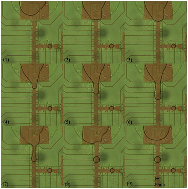
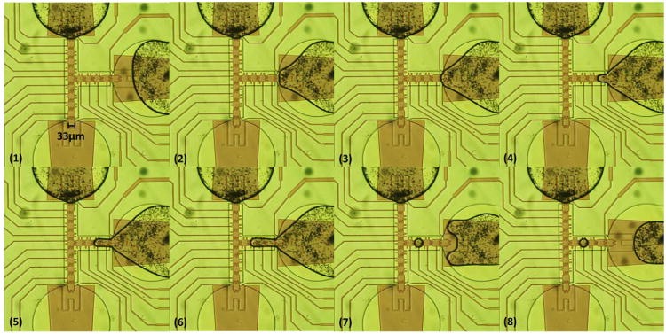
For the 33 μm electrode device with a 5 μm gasket, dispensing by extending the liquid over three electrodes was not successful, since liquid was pulled back into the reservoir. However, by using the third channel electrode (four electrodes) to split off the droplet from the extended liquid, one 18 pl droplet could be dispensed from the reservoir at 17.1 Vrms (1 kHz) with 200 nm Ta2O5 and 200 nm parylene C, as shown in Fig. 6. The reservoir's front electrode, neck electrode, and channel electrodes were turned on in sequences (Fig. 6(2)–(6)), and the droplet was cut off when the third channel electrode and reservoir electrode were on and the others off (Fig. 6(7) and (8)). The droplet volume was obtained from the top view area of the droplet, which was a circle of 69 μm in diameter multiplied by the gasket height of 5 μm.
Fig. 6.
Image sequences of droplet dispensing on 33 μm electrodes with the gasket of 5 μm. A 18 pl droplet was dispensed from a reservoir. The electrodes in the channel were turned on in sequences to pull the liquid out from the reservoir (3) to (6). The reservoir electrode and the third channel electrode were then turned on to split the droplet in (7) and (8).
The droplet size from the top view in Fig. 6 was observed to cover an entire electrode including the protrusions on each side. Comparing this situation to the droplet dispensed on 100 μm electrode device and extended over three electrodes until necking occurred, the dispensed droplet area covered only the electrode body but not the protrusions [10]. The longer necking distance does favor liquid splitting, but because the necking distance made the liquid retraction force smaller and the speed slower, the liquid volume maintained in the droplet would be larger. This result verified the concept that dispensing could be easier over a longer distance, but would result in a larger droplet volume. For 33 μm electrode devices, the droplet size was independent of the electrodes number for dispensing, because during the splitting step the liquid had already covered the entire channel electrode, the maximum area for the electrowetting force could achieve with one electrode, including the protrusions.
In addition to droplet dispensing, droplet splitting is another critical function to verify manipulation on chip. In order to have uniform splitting, the electrowetting forces on each side of the 2× droplet must be equal (or similar) in magnitude and must be applied at the same time. According to previous research [2], the electrowetting force is proportional to the applied voltage and the overlapping area of the droplet over the electrode, so that for the initial state of splitting, the 2× droplet has to be centered on the original electrode with this electrode turned on. Therefore, when the two adjacent electrodes are on, each overlap area of the 2× droplet and adjacent electrodes is equal. In addition, the two adjacent electrodes have to be simultaneously turned on, and the central electrode turned off at this time to cut off the droplet in the middle. Thus, a programmed controller was required to complete splitting without timing issues.
Despite the success in dispensing on 33 μm electrode devices with 5 μm gaskets, the droplet could not be split into two daughter droplets through the three electrode splitting protocol. During splitting of an 18 pl droplet on 33 μm electrodes with a 5 μm gasket, three electrodes with the central one off and the other two on could only form a narrow neck in the middle, but could not split the droplet. It was not possible to split a larger droplet into two 1 × droplets even when the voltage was increased to 30 Vrms, which was higher than the actuation voltage limit of 30 Vrms for the 200 nm Ta2O5 and 200 nm parylene C stack. Since the EWD device reached its actuation voltage limit, the electrowetting force could no longer increase proportionally to the voltage applied due to contact angle saturation [2]. We expected the splitting voltage should be similar to the dispensing voltage, because the cut-off mechanisms were similar. The differences between dispensing and splitting were the cut-off length, the reservoir electrode area, and the gasket neck. The cut-off approach was to stretch the liquid in opposite directions and to form a narrow neck in the middle until the neck was pinched off, as shown in Fig. 6(7) and (8). Therefore, to make dispensing possible at a relative low voltage, the dispensing protocol used three channel electrodes plus one reservoir electrode (larger area), which provided the required liquid extension and force. In addition, the gasket neck design for the reservoir opening helped the liquid pinch off the neck.
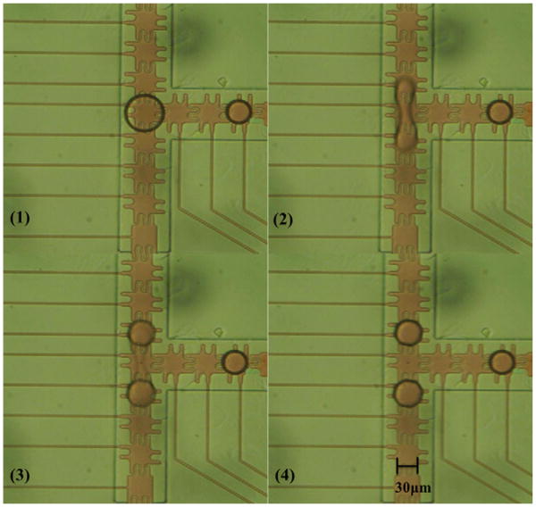
Based on the previous experience, the gasket needed to be scaled to reduce the liquid volume per electrode area, so a 3 μm gasket was fabricated on the 33 μm electrode devices and tested. Although devices with 3 μm SU8 gaskets could not seal the channel neck as well as 5 μm gaskets, the device still could dispense droplets of approximately 12 pl at the same voltage, the same dielectric insulator thickness, and the same numbers of electrodes. The volume was calculated by the same top view area of a circle 69 μm in diameter multiplying the 3 μm gasket height. Because the 12 pl droplet was big enough to overlap the two adjacent electrodes while resting on the central electrode, the splitting protocol was tested with this droplet volume. The 12 pl droplet was split into two 6 pl droplets at 18.7 Vrms, as shown in the series pictures in Fig. 7.
Fig. 7.
Image sequences of droplet splitting on 33 μm electrodes with the 3 μm height gasket. One 12 pl droplet (2× droplet) were dispensed from a reservoir to the position in (1). Two adjacent electrodes were turned on with 18.7 Vrms to split into two 6 pl droplets simultaneously.
4.2. 21 μm electrodes
When designing the 33 μm electrode devices, the overall area of the EWD device was mostly determined by the 22 pins of the control pads, and so the device size was set at 2 cm × 3 cm. Since the actual active region for electrodes is reduced by scaling, a 33 μm and a 21 μm device could be fabricated together on a single chip, and each device had its own control pads on one long edge. As a result, once the fabrication process was completed, two different devices could be tested on a single chip.
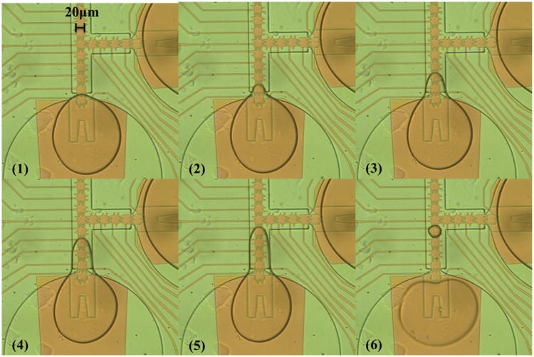
Two different gasket thicknesses of 5 μm and 3 μm could be also examined on the 21 μm electrode shown in Fig. 3. For the 5 μm gasket devices, the same issue occurred, whereby the liquid could be pulled out of the reservoir, but could not be cut off, even when extended across the distance of all 7 electrodes in the channel. In each attempt, all the liquid would be dragged back to the reservoir when the reservoir electrode was turned on. Therefore, a thinner, 3 μm, gasket was then tested. The sealing quality at the reservoir neck of a 3 μm gasket on a 21 μm electrode device was worse than that on a 33 μm electrode device. Despite the poor sealing, a droplet of approximately 5 pl was still able to be dispensed at 22 Vrms as demonstrated in Fig. 8 (Video 1). However, due to the sealing issue, the liquid being pulled out of the reservoir overflowed the reservoir neck and the required narrow neck was not formed, as shown in Fig. 8(3)–(5). As a result, four electrodes were not enough to split the droplet from the reservoir, so that the fifth electrode (Fig. 8(6)) and a higher voltage (compared to the same thickness of dielectric layers on other scale devices) were required to hold the droplet on the electrode from the retraction force of liquid as the reservoir electrode was on. Although dispensing was reproducible on 21 μm electrode devices with 3 μm gaskets, splitting could not be accomplished. The 2 × droplet could not be cut off at 30 Vrms, which was above the actuation voltage limit. This issue was also observed in previous devices, so further scaling of the gaskets was needed. Therefore, a 1 μm SU8 gasket was fabricated and tested on a 21 μm electrode device, but this gasket was too thin to maintain liquid in the reservoir area with pressure sealing, even on a NOA coated top plate. While dispensing liquid from a pipette into an on-chip reservoir, liquid would overflow and spread over the entire device.
Fig. 8.
Image sequences of droplet dispensing on 21 μm electrodes with the gasket of 3 μm. A 5 pl droplet was dispensed from a reservoir at 22 Vrms. The electrodes in the channel were turned on in sequences to pull the liquid out from the reservoir, from (2) to (5). The reservoir electrode was turned on to split the droplet in (6). Because of the poor sealing, the liquid being pulled out of the reservoir overflowed the gasket neck and no narrow neck was formed (3)–(5), and five electrodes and a higher voltage were required to dispense.
During the experiments of fabricating and testing the picoliter scale devices, all the manipulations of scaling devices were operated on chip without any external forces, relying only on electrowetting forces. Although many different parameters, such as types of surfactants, liquid volumes, and gasket thicknesses and designs needed to be considered in real situations while dispensing and splitting, the results of these studies verified and demonstrated the basic theories and concepts of scaling EWD devices.
4.3. EWD actuator implementation
DNA pyrosequencing has been demonstrated in both nanoliter and 300 pl EWD devices [17,18]. For a simplified verification, DNA pyrosequencing on EWD devices included manipulation of paramagnetic beads and buffer solutions with luciferase and ATP with luciferin. Here, these solutions were also demonstrated on the scaled devices of 33 μm and 21 μm electrodes. Invitrogen Dynabeads M-270 2.8 μm streptavidin-functionalized paramagnetic bead solution was dispensed into the reservoir, and droplets could be dispensed on chip into the channel for both devices with 3 μm gaskets. A 12 pl bead droplet was dispensed on a 33 μm electrode device, as shown in Fig. 9. The dispensing voltages were the same as needed for DI water manipulation mentioned above. Reservoirs containing buffer solutions of 1 μg/μl luciferase and 400 μg/ml luciferin with 0.1 μM ATP [18] were dispensed as droplets on both 33 μm and 21 μm electrode EWD devices.
Fig. 9.
2.8 μm paramagnetic beads in a 12 pl droplet were dispensed from a reservoir on a 33 μm electrode device with a 3 μm gasket. The bead solution was first dispensed into the reservoir with a pipette. The electrodes in the channel were turned on in sequences to pull the bead solution out from the reservoir (3) to (6). The reservoir electrode and the third channel electrode were then turned on to split the bead droplet in (7) and (8).
In the pyrosequencing reaction, the amount of pyrophosphate (PPi) produced by the incorporation reaction between DNA and nucleotides is a linear response to the amount of nucleotides reacted. ATP, which is produced by an enzymatic reaction with PPi, is used in the chemiluminescent reaction that produces light that allows the amount of nucleotides reacted to be determined during the sequencing of unknown DNA. Using an externally mounted cooled CCD camera (CoolSnap ES2, Photometrics) mounted with a 10× objective (Epiplan-Neofluar), we were able to create a calibration curve relating light intensity versus reactant ATP concentration on 300 pl chips [18]. For 100 pl chips, the light intensity decreased by about 1/3.
As the device dimensions are further scaled, the ATP-luciferin reaction was implemented on 33 μm and 21 μm electrode devices with 3 μm and 5 μm gaskets. Both substrate and enzyme solutions could be successfully dispensed and merged on all these devices (Video 2) with the same concentrations used for 100 pl droplet reactions, but the resulting light intensity was too low to be detected by the external cooled CCD camera even with long exposure times and 8 × 8 pixel binning. As an alternative to the cooled CCD camera, an EMCCD camera (QuantEM, Photometrics), whose working temperature is −30 °C and quantum efficiency at 560 nm wavelength is 92%, was also tested as a sensor of the chemiluminescent signal, but no light could be detected with such small droplet volumes. These results suggest that better coupling of light out of the droplet itself is required using integrated sensors built into the top plate of the actuator, as demonstrated by Luan et al. [19]. However, the EWD actuator was demonstrated and verified as a platform to manipulate picoliter droplets on demand, and could be implemented to different applications in the future.
5. Conclusions
The work reported in this study has demonstrated dimensional scaling of EWD actuators into the picoliter volume range. Picoliter actuator fabrication has required new multi-layer insulator structures, interleaved electrode design to increase electrowetting forces, and improved gasket designs to allow for the sealing of the two plate sandwich actuator as well as adequate flow focusing for dispensing droplets from on-chip reservoirs. With dielectric layers of 200 nm Ta2O5 and parylene C, the results of different electrode sizes and gasket thicknesses are listed in Table 1. The droplet size of 5 pl is the smallest volume reported in view of all the EWD microfluidic research results published up to date. In addition, paramagnetic beads and buffer solutions with luciferase and luciferin with ATP were manipulated on these scaled devices. These results have demonstrated that the scaled EWD actuators can be implemented in real biomedical or biochemical applications.
Table 1.
The results of scaled EWD devices. The cross line means splitting failures.
| Electrode size (μm) | Gasket thickness (μm) | Droplet size (pl) | Dispensing voltage (Vrms) | Splitting voltage (Vrms) |
|---|---|---|---|---|
| 100 [10] | 20 | 300 | 11.4a | – |
| 15 | 200 | 17.7 | 17.7 | |
| 33 | 5 | 18 | 17.1 | – |
| 3 | 12 | 17.1 | 18.7 | |
| 21 | 3 | 5 | 22 | – |
The dielectric layer are 135 nm Ta2O5 and 180 nm parylene C.
These results also show that two plate EWD devices are feasible for gasket thicknesses smaller than 10 μm. However, the physical scaling of EWD devices appears to face a significant difficulty in confining liquid in a reservoir with a gasket thinner than 3 μm. In addition, dispensing liquid from a macro-scale pipette onto the nano-scale on-chip reservoir becomes a challenge due to the limited capillary filling for 3 μm gaskets. Despite this sealing problem, we believe the electrowetting theory is still viable for smaller scale electrodes, but due to the electrode-size-to-channel-height ratio, the submicron dimension channel fabrication would be the key obstacle to overcome.
Supplementary Material
Acknowledgments
This research was supported by grant # R01HG004354-01 from the National Institutes of Health.
Biographies
Yan-You Lin received his B.S. degree in electronics engineering from National Chiao Tung University, Taiwan in 2004; M.S. degree in electrical engineering from National Taiwan University, Taipei, Taiwan, in 2006; Ph.D. degree in electrical and computer engineering from Duke University, Durham, NC, in 2011. His research interests include microfluidics, lap-on-a-chip technologies, and microsystems design.
Erin R.F. Welch received her PhD in analytical chemistry from the University of North Carolina at Chapel Hill in 2009. She was a postdoctoral fellow in Electrical and Computer Engineering at Duke University, with interests in general microfluidics, digital electrowetting, DNA sequencing and analysis.
Richard B. Fair is a Lord-Chandran Professor of Engineering at Duke. His current research areas include digital microfluidic devices, applications, and technology. He has published over 150 papers in refereed journals and conference proceedings, written 11 book chapters, edited nine books or conference proceedings, and given over 130 invited talks. Dr. Fair is also a Fellow of the IEEE, a Fellow of the Electrochemical Society, past Editor-in-Chief of the Proceedings of the IEEE, and he has served as associate editor of the IEEE Transactions on Electron Devices. He is a recipient of the IEEE Third Millennium Medal (2000) and the 2003 Solid State Science and Technology Prize and Medal from the Electrochemical Society, which was presented in Paris.
Footnotes
Appendix A. Supplementary data: Supplementary data associated with this article can be found, in the online version, at http://dx.doi.org/10.1016/j.snb.2012.07.022.
References
- 1.Fair RB. Digital microfluidics: is a true lab-on-a-chip possible? Microfluidics and Nafluidics. 2007;3(3):245–281. [Google Scholar]
- 2.Song JH, Evans R, Lin YY, Hsu BN, Fair RB. A scaling model for electrowetting-on-dielectric microfluidic actuators. Microfluidics and Nafluidics. 2009;7:75–89. [Google Scholar]
- 3.Pollack MG, Fair RB, Shenderov AD. Electrowetting-based actuation of liquid droplets for microfluidic applications. Applied Physics Letters. 2000;77(11):1725–1727. [Google Scholar]
- 4.Tabeling P. Introduction to Microfluidics. Oxford University Press; New York: 2005. [Google Scholar]
- 5.Cho SK, Fan SK, Moon H, Kim CJ. Towards digital microfluidic circuits: creating, transporting, cutting and merging liquid droplets by electrowetting-based actuation. Proceedings IEEE Micro Electro Mechanical Systems. 2002;11:454–461. [Google Scholar]
- 6.Cho SK, Moon H, Kim CJ. Creating, transporting, cutting, and merging liquid droplets by electrowetting-based actuation for digital microfluidic circuits. Journal of Microelectronic Systems. 2003;12(1):70–80. [Google Scholar]
- 7.Pollack MG. PhD Thesis. Duke University; 2001. Electrowetting-based microactuation of droplets for digital microfluidics. [Google Scholar]
- 8.Pollack MG, Shenderov AD, Fair RB. Electrowetting-based actuation of droplets for integrated microfluidics. Lab on a Chip. 2002;2:96–101. doi: 10.1039/b110474h. [DOI] [PubMed] [Google Scholar]
- 9.Li Y, Parkes W, Haworth LI, Stokes AA, Muir KR, Li P, Collin AJ, Hutcheon NG, Henderson R, Rae B, Walton AJ. Anodic Ta2O5 for CMOS compatible low voltage electrowetting-on-dielectric device fabrication. Solid State Electronics. 2008;52:1382–1387. [Google Scholar]
- 10.Lin YY, Evans RD, Welch E, Hsu BN, Madison AC, Fair RB. Low voltage electrowetting-on-dielectric platform using multi-layer insulators. Sensors and Actuators B. 2010;150(1):465–470. doi: 10.1016/j.snb.2010.06.059. [DOI] [PMC free article] [PubMed] [Google Scholar]
- 11.Zhang T, Chakrabarty K, Fair RB. Behavioral modeling and performance evaluation of microelectrofluidics-based PCR systems using System C. IEEE Transactions on Computer-Aided Design of Integrated Circuits and Systems. 2004;23(6):843–858. [Google Scholar]
- 12.Pollack MG, Paik PY, Shenderov AD, Pamula VK, Dietrich FS, Fai RB. Investigation of electrowetting-based microfluidics for real-time PCR applications. Proceedings of Micro Total Analysis Systems; 2003; pp. 619–622. [Google Scholar]
- 13.Srinivasan V, Pamula VK, Fair RB. An integrated digital microfluidic lab-on-a-chip for clinical diagnostics on human physiological fluids. Lab on a Chip. 2004;4:310–315. doi: 10.1039/b403341h. [DOI] [PubMed] [Google Scholar]
- 14.Moon H, Wheeler AR, Garrell RL, Loo JA, Kim CJ. An integrated digital microfluidic chip for multiplexed proteomic sample preparation and analysis by MALDI-MS. Lab on a Chip. 2006;6(9):1213–1219. doi: 10.1039/b601954d. [DOI] [PubMed] [Google Scholar]
- 15.Lin HC, Liu YJ, Yao DJ. Core shell droplets for parallel DNA ligation of an ultra-micro volume using an EWOD microfluidic system. Journal of Laboratory Automation. 2010;15(3):210–215. [Google Scholar]
- 16.Cho SK, Zhao Y, Kim CJ. Concentration and binary separation of micro particles for droplet-based digital microfluidics. Lab on a Chip. 2007;7:490–498. doi: 10.1039/b615665g. [DOI] [PubMed] [Google Scholar]
- 17.Boles DJ, Benton JL, Siew GJ, Levy MH, Thwar PK, Sandahl MA, Rouse JL, Perkins LC, Sudarsan AP, Pamula VK, Srinivasan V, Fair RB, Griffin PB, Eckhardt AE, Pollack MG. Droplet-based pyrosequencing using digital microfluidics. Analytical Chemistry. 2011;83(22):8439–8447. doi: 10.1021/ac201416j. [DOI] [PMC free article] [PubMed] [Google Scholar]
- 18.Welch ERF, Lin YY, Madison A, Fair RB. Picoliter DNA sequencing chemistry on an electrowetting-based digital microfluidic platform. Biotechlogy Journal. 2011;6:165–176. doi: 10.1002/biot.201000324. [DOI] [PMC free article] [PubMed] [Google Scholar]
- 19.Luan L, Evans R, Jokerst NM, Fair RB. Integrated optical sensor in a digital microfluidic platform. IEEE Sensors Journal. 2008;8:628–635. [Google Scholar]
- 20.Srinivasan V, Pamula VK, Fair RB. Droplet-based microfluidic lab-on-a-chip for glucose detection. Analytica Chimica Acta. 2004;507(1):145–150. [Google Scholar]
- 21.Lin YY, Lin CW, Yang LJ, Wang AB. Micro-viscometer based on electrowetting on dielectric. Electrochimica Acta. 2007;52:2876–2883. [Google Scholar]
- 22.Moon H, Cho SK, Garrell RL, Kim CJ. Low voltage electrowetting-on-dielectric. Journal of Applied Physics. 2002;92(7):4080–4087. [Google Scholar]
- 23.Nelson WC, Kim CJ. Monolithic fabrication of EWOD chips for picoliter droplets. Journal of Microelectronic Systems. 2011;20:1419–1427. [Google Scholar]
- 24.Lippmann MG. Relations entre les phénomènes electriques et capillaires. Annales de chimie et de physique. 1875;5(11):494–549. [Google Scholar]
- 25.Berge B. Electrocapillarite et mouillage de films isolants par l'eau. Comptes rendus de l'Académie des sciences. 1993;317(2):157–163. [Google Scholar]
- 26.Berthier J. Microdrops and Digital Microfluidics. William Andrew; New York: 2008. [Google Scholar]
Associated Data
This section collects any data citations, data availability statements, or supplementary materials included in this article.


