Abstract
ZnO/Al2O3 multilayers were prepared by alternating atomic layer deposition (ALD) at 150°C using diethylzinc, trimethylaluminum, and water. The growth process, crystallinity, and electrical and optical properties of the multilayers were studied with a variety of the cycle ratios of ZnO and Al2O3 sublayers. Transparent conductive Al-doped ZnO films were prepared with the minimum resistivity of 2.4 × 10⁻³ Ω·cm at a low Al doping concentration of 2.26%. Photoluminescence spectroscopy in conjunction with X-ray diffraction analysis revealed that the thickness of ZnO sublayers plays an important role on the priority for selective crystallization of ZnAl2O4 and ZnO phases during high-temperature annealing ZnO/Al2O3 multilayers. It was found that pure ZnAl2O4 film was synthesized by annealing the specific composite film containing alternative monocycle of ZnO and Al2O3 sublayers, which could only be deposited precisely by utilizing ALD technology.
Keywords: Aluminum-doped zinc oxide, Zinc aluminate, Atomic layer deposition, X-ray diffraction, Photoluminescence
Keywords: 81.15.Gh, 72.20.Jv, 78.20.Ci
Background
In the ZnO-Al2O3 composite material system, Al-doped zinc oxide (AZO) and zinc aluminate (ZnAl2O4) spinels are well known for their applications in optoelectronic devices and chemical industry. AZO was considered as an alternative low-cost transparent conductive oxide material instead of indium tin oxide in photovoltaic cells and displays [1,2]. ZnAl2O4 material has been used in many catalytic reactions, such as cracking, dehydration, hydrogenation, and dehydrogenation reactions [3,4]. As a wide-bandgap semiconductor material, ZnAl2O4 was also used as host of phosphors doping with Mn and rare earth ions [5,6]. AZO and ZnAl2O4 thin films have been deposited by different techniques [7], such as sol–gel coating [8], pulsed laser deposition [9], chemical vapor deposition [10], radio-frequency sputtering [11], and atomic layer deposition (ALD) [12,13]. Recently, ALD technology has been employed to grow transparent conductive AZO films with low resistivity in the order of 10−3 Ω·cm [14,15]. However, the correlation between the optical and the electrical properties in the ALD of AZO films has not yet been understood very well. Meanwhile, ZnAl2O4 film deposited on porous or nanostructure supporting materials by ALD technology may have large surface area and potential applications in catalysts and phosphors. However, since the ZnAl2O4 films need to be synthesized by annealing ZnO/Al2O3 composite films at elevated temperatures, the preferable crystallization of ZnO in the ALD of ZnO/Al2O3 composite films may strongly influence the purity of the synthesized ZnAl2O4 films. A detailed study on the correlation between the ZnO/Al2O3 cycle ratios in the multilayers and the formation of ZnO and ZnAl2O4 crystal phases during the subsequent thermal annealing would be crucial for synthesizing high purity ZnAl2O4 films.
In this paper, the ALD processes of the Al2O3 and ZnO thin films were studied using diethylzinc (DEZn), trimethylaluminum (TMA), and water with a variety of substrate temperatures. The growth temperature of the ZnO/Al2O3 composite films was determined by optimizing the growth temperature of ZnO layer according to the photoluminescence (PL) spectroscopy analysis. Then AZO films were prepared by adding a small fraction of Al2O3 doping cycles in the ALD process of ZnO films. The dependences of the crystalline structure, resistivity, and optical band gap of the AZO films on the Al doping concentration were studied in detail. Afterwards, multiple crystalline ZnAl2O4 films were synthesized by annealing the ALD ZnO/Al2O3 multilayers with a high fraction of Al2O3 layers. The influences of the ALD cycle ratio of the ZnO/Al2O3 sublayers and the annealing temperature on the formation of ZnO and ZnAl2O4 phases were studied by X-ray diffraction analysis. PL spectroscopy was used in conjunction with X-ray diffraction (XRD) to analyze traceable ZnO phase in thermal processed samples. It was found that pure ZnAl2O4 film was synthesized by annealing the specific composite film containing alternative monocycle of ZnO and Al2O3 sublayers, which could only be deposited precisely utilizing ALD technology.
Methods
ZnO/Al2O3 composite films were deposited on quartz glass substrates or n-type Si substrates with (100) orientation. Before the film deposition, the Si substrates were cleaned through the Radio Corporation of America process, and the quartz glass substrates were treated by ultrasonic cleaning in alcohol and acetone. The ALD equipment is a 4-in. small chamber ALD system (Cambridge NanoTech Savannah 100, Cambridge NanoTech Inc., Cambridge, MA, USA). Diethylzinc (DEZn Zn(C2H5)2) and TMA Al(CH3)3 were used as the metal precursors for ZnO and Al2O3, respectively, while water vapor was used as oxidant. During the ALD process, the DEZn and TMA sources were not intentionally heated, and the precursor delivery lines were kept at 150°C. Nitrogen (99.999%) was used as carrier and purge gas with a flow rate of 20 sccm. One ZnO cycle consists of 0.015 s DEZn pulse time, 5 s N2 purge, 0.02 s H2O pulse time, and 5 s N2 purge. One Al2O3 cycle has 0.015 s TMA pulse time, 5 s N2 purge, 0.02 s H2O pulse time and 5 s N2 purge. First, pure ZnO and Al2O3 films were deposited on Si substrates with a variety of the growth temperature from 100°C to 350°C to determine the ALD windows. Then AZO films were deposited on quartz glass substrates at a temperature of 150°C. The total ALD cycles of ZnO plus Al2O3 layers are 1,090 for all the AZO samples, and the ALD cycles of the ZnO and Al2O3 sublayers in AZO films are varied with 50/1, 22/1, 20/1, 18/1, 16/1, 14/1, 12/1, and 10/1, respectively. For the ZnO/Al2O3 composite films with high fraction of Al2O3 sublayers, the total ALD cycles of the multilayers are 1,002, and the ALD cycles of the ZnO and Al2O3 sublayers are varied with 5/1, 4/1, 3/1, 2/1, 1/1, and 1/2, respectively. In order to synthesize crystalline ZnAl2O4 spinel films, the as-grown composite films were annealed subsequently in air at 400, 600, 700, 800, 1,000, and 1,100°C for 30 min, respectively.
The crystal structures of the samples were characterized by XRD analysis with Cu Kα radiation. The resistivity of the AZO films deposited on quartz substrate was measured using four-point probe technique. Transmission spectra were taken by a spectrometer with a 150 W Xe lamp. The thickness and the refractive index of the ZnO/Al2O3 composite films were measured by an ellipsometer with a 632.8-nm He-Ne laser beam at an incident angle of 69.8°. The average film growth per cycle was calculated by dividing the film thickness by the total number of ALD cycles. PL spectra from the films were measured at room temperature under the excitation of the 266 nm line of a Q-switch solid state laser (CryLas DX-Q; CryLaS GmbH, Berlin, Germany). The PL signal was collected by a 1/2-m monochromator and detected by a photomultiplier (model H7732-10) connected to a computer controlled Keithley 2010 multimeter (Keithley Instruments Inc., Cleveland, OH, USA). The topography of the ZnAl2O4 films was observed using a scanning electron microscope (SEM).
Results and discussion
Growth temperature of the ZnO/Al2O3 composite films
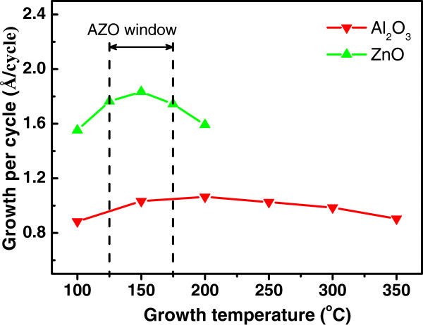
In order to determine the common ALD growth temperature for ZnO/Al2O3 multilayers, the dependences of the growth per cycle on the substrate temperatures were studied on pure ZnO and Al2O3 films, respectively, as shown in Figure 1. The growth per cycle of the ZnO film increases from 1.55 to 1.83 Å as the deposition temperature increases from 100°C to 150°C, and then decreases to 1.59 Å as the temperature increases to 200°C, indicating a narrow ALD growth window of ZnO around 150°C with growth rate of 1.83 Å/cycle. The thermal dependence of the growth rate of Al2O3 shows a nearly constant value at around 1.0 Å/cycle in a wide temperature window from 100°C to 350°C. The optimized growth temperature for growth of uniform ZnO/Al2O3 multilayer should be optimized within the overlap region of the two ALD windows. Optimization should be done according to the growth temperature for high-quality ZnO films.
Figure 1.
Dependences of the growth per cycle of pure ZnO and Al2O3 films on the growth temperatures.
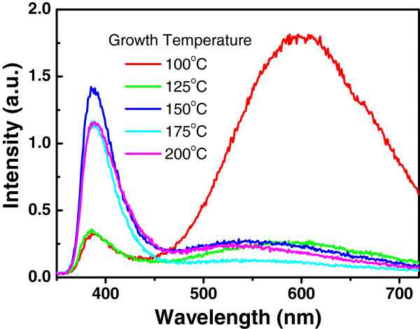
The crystal quality of a semiconductor is normally evaluated by the efficiency of its band-edge photoluminescence; therefore, room temperature PL spectra of the ZnO films grown at different temperature were studied under the excitation of a 266-nm laser, as shown in Figure 2. The ultraviolet (UV) peak at around 387 nm is from the near-band-edge emission of crystalline ZnO, while the broad peak around 600 nm can be ascribed to the radiative recombination at the defects in ZnO films. The intensity of the UV peak increases with increasing the growth temperature from 100°C to 150°C, with a maximum growth temperature at 150°C and saturation at higher growth temperature up to 200°C. In the meantime, the luminescent band at 600 nm from the defects strongly decreases from 100°C to 150°C. This indicates that the crystalline quality of the ZnO film is getting better with a decrease of the defect density from 100°C to 150°C and become stable at higher growth temperatures up to 200°C. Luca et al. [16] reports an increase of the PL intensity with further increasing growth temperature from 200°C to 240°C, indicating a better crystal quality of the ZnO film at higher growth temperature. However, ZnO films cannot be deposited uniformly in ALD mode at higher temperatures above 200°C due to the thermal decomposition of DEZn precursor [17]. As a consequence, the optimized growth temperature for deposition of ZnO/Al2O3 composite films was selected at 150°C. The growth rates of the pure ZnO and Al2O3 films were 1.83 and 1.03 Å per cycle at this temperature, respectively, which are consistent with the reported values in [18].
Figure 2.
Room temperature PL spectra from the ZnO films with different growth temperatures.
The AZO films
AZO films with overall 1,090 cycles of ZnO plus Al2O3 layers were alternatively deposited on quartz substrates at 150°C. The ALD cycles in the ZnO/Al2O3 supercycles are 50/1, 22/1, 20/1, 18/1, 16/1, 14/1, 12/1, and 10/1, where monocycle Al2O3 doping layers were inserted between different cycles of ZnO sublayers. Since the real Al concentration matches the ‘rule of mixtures’ formula well at lower Al concentration below 5%, in which the growth rate of the AZO is close to pure ZnO [19]. The Al concentration in the AZO films was calculated using the following formula:
| (1) |
where is the percentage of Al2O3 cycles, ρAl, and ρZn are the densities of Al and Zn atoms deposited during each ALD cycle for the pure Al2O3 and ZnO films, respectively. The densities of Al2O3 and ZnO growth by ALD are 2.91 and 5.62 g/cm3[20], So ρAl and ρZn were calculated to be 5.89 × 10⁻¹⁰ mol/cm2/cycle and 1.27 × 10⁻⁹ mol/cm2/cycle, respectively.
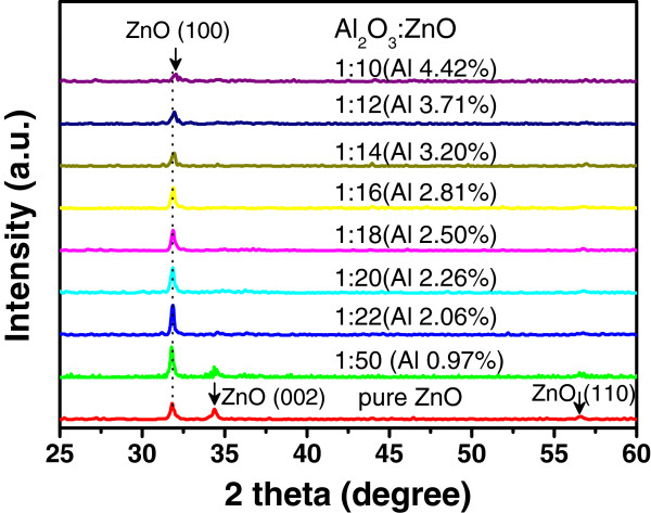
Figure 3 shows the XRD patterns of the AZO films grown on quartz substrate with different ZnO/Al2O3 cycle ratios that are varied from 50:1 to 10:1 (corresponding to Al concentration from 0.96% to 4.42%). The diffraction pattern of the pure ZnO film without Al2O3 doping layer is also shown as a reference. The X-ray diffraction pattern from pure ZnO film exhibits multiple crystalline ZnO structure with (100), (002), and (110) peaks [17]. With increasing the Al doping concentration, the (002) and (110) diffraction peaks decrease strongly, thus the AZO films exhibiting (100) dominated the orientation. The intensity of the (100) diffraction peak reaches a maximum at 2.06% (with the ratio of ZnO/Al2O3 layers is 22/1), and then it decreases at higher Al concentration above 3%. The preferred (100) orientation of the AZO films in our samples is consistent with the results reported by Banerjee et al. [18]. It is worthy to note that the Al2O3 layer by ALD is amorphous at the growth temperature of 150°C, so the decrease of the (100) peak at higher Al concentration can be explained that the amorphous Al2O3 doping layers destroy the crystal quality during the growth of AZO films. Figure 3 also shows that the (100) peak of ZnO shifts to larger diffraction angle with increasing the concentration of Al in AZO films. This can be interpreted as that the increase of the Al concentration will reduce the lattice constant by substitutions of Zn2+ ions (ion radius 0.74 Å) with smaller Al3+ (0.53 Å) ions; therefore, the (100) peak of ZnO shifts to larger diffraction angle in AZO films.
Figure 3.
XRD patterns of the AZO films with different Al content from 0% to 4.42%.
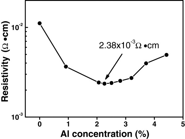
Figure 4 plots the resistivity of AZO films as a function of Al concentration, which was measured by four-point probe technique. As the Al concentration increases from 0% to 2.26%, the resistivity initially decreases from 1.11 × 10⁻² to a minimum of 2.38 × 10⁻³ Ω·cm, and then increases at higher Al doping concentration. This result is comparable to the values of the ALD grown AZO films reported by other groups [12,14,21]. The decreasing of the resistivity may attribute to the increase of Al donor concentration by substitution of Zn2+ sites with Al3+ ions in the ZnO lattices. However, it should be noted that the variety of resistivity in Figure 4 is also in strong correlation to the change of crystal quality in the AZO films at different Al doping concentrations, as shown in Figure 3. Initially, the decrease of the resistivity with increasing the Al concentration from 0% to 2.26% is related to the improvement of the crystal quality of the AZO films, as it was indicated by the increased intensity of the (100) X-ray diffraction peak in Figure 3. The AZO film with the best crystal quality has the minimum resistivity of 2.38 × 10⁻³ Ω·cm at Al concentration of 2.26%. At higher Al doping concentration above 3%, a decrease of the intensity of the (100) diffraction peak indicates a degeneration of the crystal quality; as a consequence, an increase of the resistivity was shown in Figure 4. The reason for the increase of the resistivity at high Al concentration is probably related to the formation of Zn vacancy acceptors or the formation of homologous phase like ZnAlxOy or Al2O3 in the AZO films [9,22].
Figure 4.
Dependence of the resistivity of AZO films on Al concentration.
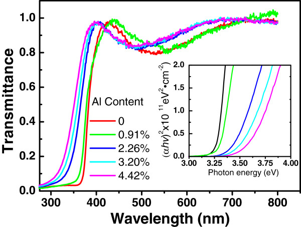
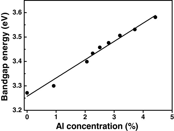
The transmission spectra of the AZO films deposited on quartz glasses are shown in Figure 5. The average transmittance was above 80% in the visible wavelength, regardless of the Al concentration in the AZO films. A blue shift of the optical band edge was observed with increasing the Al concentration. The relationship between absorption coefficient and optic band gap of direct band gap semiconductor is given by Tauc equation [23], (αhv)2 = B(hv − Eg), where α is the absorption coefficient, hν is the photon energy, B is a constant, and Eg is the optical band gap energy, respectively. The dependence of (αhν)2 on photon energy was plotted in the inset of Figure 5. The band gap energy was obtained by the extrapolations of the liner regions of the optical absorption edges. Figure 6 shows the variation of band gap energy versus Al concentration. The band gap energy increased from 3.27 to 3.58 eV with increasing Al concentration from 0% to 4.42%. A linear fit to the bandgap energy versus Al concentration gives Eg= 3.26 + 0.0749xAl, where Eg is the band gap energy of AZO, xAl is the Al concentration of AZO. The correlation between the blue shift of the absorption edge and the increased conductivity with Al doping can be attributed to the Bustein-Moss increase of the band gap with increasing carrier concentration in semiconductors [12].
Figure 5.
Transmission spectra of AZO films deposited on quartz glasses. The inset is the plots of (αhν)2 versus photon energy.
Figure 6.
Dependence of the band gap energy of AZO films on Al concentration.
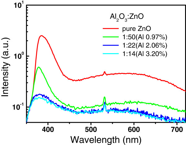
Figure 7 shows the room temperature PL spectra excited by a 266-nm laser for AZO films with different Al concentrations. The blue shift of the UV peaks from the near-band-edge emission of ZnO is consistent with the results from the transmittance spectra in Figure 5 and Figure 6. The intensity of the PL decreases strongly with increase of the Al concentration from 0% to 3.2% in the as-prepared AZO films. This is probably due to the introduction of the nonradiative recombination centers with increasing fraction of the amorphous Al2O3 doping layers in AZO films.
Figure 7.
Room temperature PL spectra excited by a 266-nm laser for AZO films with different Al concentration.
ZnAl2O4 films
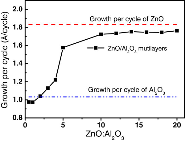
Starting ZnO/Al2O3 composite films with high fraction of Al2O3 layers were grown by ALD prior to synthesis of the ZnAl2O4 films by high temperature annealing process. Figure 8 shows the dependence of the average growth per cycle on the ZnO/Al2O3 cycle ratio in the multilayers. The average growth per cycle of the composite films at ZnO/Al2O3 ratio of 1:2 and 1:1 is smaller than the growth rate of pure ZnO and Al2O3 layers. The reason is that there is a strong etching of the pre-deposited ZnO layer during exposure ZnO surface to the TMA precursor in the ALD cycle of Al2O3, as discussed in detail in [18,19]. The removal of the ZnO surface layer causes a reduction of average growth rate especially when the thickness of the ZnO sublayers reduces to several cycles. The influence of the surface etching of ZnO sublayer on the growth rate can be eliminated by increasing the thickness of the ZnO sublayer. This is observed by the strong increase of the average growth per cycle with increasing ZnO sublayer thickness from 1 to 10 cycles in Figure 8. The average growth rate is almost constant at around 1.75 Å/cycle during the ALD ZnO/Al2O3 multilayers when the ALD cycles of the ZnO/Al2O3 sublayers is above 10:1, which is close to the growth rate of pure ZnO (1.838 Å/cycle).
Figure 8.
Dependence of the growth per cycle of the ZnO/Al2O3 composite films on the ZnO/Al2O3 cycle ratio.
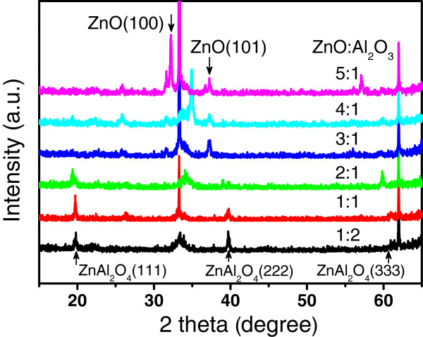
Attention has been paid to select the starting specific ZnO/Al2O3 composite films with appropriate sublayer thicknesses for synthesizing pure ZnAl2O4 films. ZnO/Al2O3 multilayers with different ZnO/Al2O3 cycle ratios from 1:2 to 5:1 were grown by ALD and then subsequently annealed at 1,000°C for 0.5 h. Figure 9 shows the XRD patterns of the annealed samples with different ZnO/Al2O3 cycle ratios. The XRD patterns of the annealed composite films show (111), (222), and (333) peaks of ZnAl2O4 spinel structure for the ZnO/Al2O3 cycle ratios at 2:1, 1:1, and 1:2 respectively, indicating that only ZnAl2O4 films with spinel crystal structure are synthesized from these specific ZnO/Al2O3 starting multilayers by ALD. A competition process of the easy ZnO crystallization with the formation of crystalline ZnAl2O4 is observed with the increasing thickness of ZnO sublayer. It should be noted that only the (100) and (101) peaks of the hexagonal phase ZnO appear and no crystalline Al2O3 or ZnAl2O4 peaks are detectable in the X-ray diffraction patterns of the samples with cycle ratio of 3:1, 4:1, and 5:1, where the ZnO sublayer thickness is more than three ALD cycles. This reveals that the thickness of the ZnO sublayer in the ZnO/Al2O3 composite films is a crucial parameter for the control of the formation of ZnO and ZnAl2O4 phases during the thermal annealing process. Taking into account of the etching during the Al2O3 cycle, the measured ZnO sublayer thickness is 0.91 and 2.01 Å in the samples with the ZnO/Al2O3 cycle ratios of 2:1 and 1:1. Comparing to the reported length of the Zn-O bond (1.98 Å) [24], the critical thickness of the ZnO sublayer is limited within one atomic layer for the formation of the ZnAl2O4 phase. This can be interpreted by the chemical reaction for synthesis of the ZnAl2O4, ZnO + Al2O3 = ZnAl2O4, where one monolayer of Al2O3 consumes one atomic layer of ZnO. Thicker ZnO sublayer containing excess atomic layers has a priority forming in the ZnO crystal phase of the annealed ZnO/Al2O3 multilayers, because the crystallization of ZnO need much lower energy than that for the ZnAl2O4 crystallization.
Figure 9.
XRD patterns of the compound films at different ZnO/Al2O3 cycle ratios.
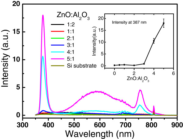
Room temperature PL spectroscopy was used to analyze and control traceable amount of the crystalline ZnO phase in the annealed samples. Figure 10 shows the PL spectra from the ZnO/Al2O3 mutilayers annealed at 1,000°C with different cycle ratios of ZnO/Al2O3 from 1:2 to 5:1. No PL signal from the crystalline ZnO is observed for the annealed samples with the ZnO/Al2O3 cycle ratios at 2:1, 1:1, and 1:2, respectively; this is supported by the XRD results in Figure 9, which showed only diffraction peaks of spinel ZnAl2O4 without ZnO impurity phase in these samples. The PL intensity from ZnO near-band-edge emission increases strongly as the ZnO sublayer thickness increases above three ALD cycles; this is also in good agreement with the formation of ZnO phase in the samples with ZnO/Al2O3 ratios of 3:1 to 5:1. These results reveal that the presence of excess ZnO bonds leads to the formation of the ZnO crystal phase due to the easy crystallization of ZnO. The specific multilayers containing alternative monatomic layers of ZnO and Al2O3 are crucial as the starting composite for synthesis of pure ZnAl2O4 films. The composite can only be deposited precisely through layer by layer ALD technology. Preformation of Zn-O-Al-O bonds at the interface of two ZnO/Al2O3 multilayers during the ALD process may play an important role for the crystallization of pure ZnAl2O4 films in the subsequent high-temperature annealing.
Figure 10.
Room temperature PL spectra of the ZnO/Al2O3 composite films with different ZnO/Al2O3 cycle ratios.
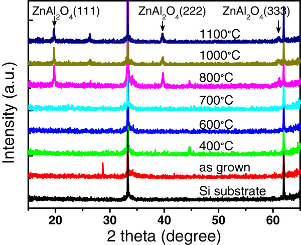
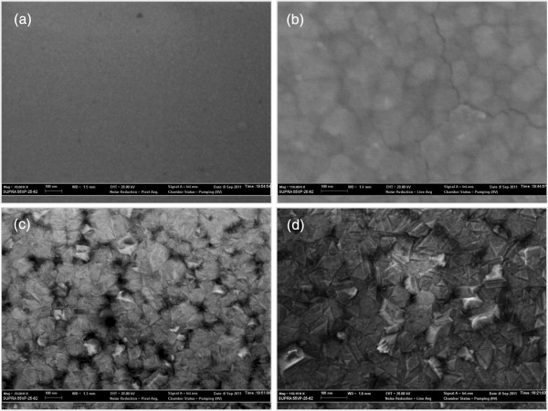
Figure 11 shows the XRD patterns of the composite films after annealed at different temperatures ranging from 400 to 1,100°C, in which the ZnO/Al2O3 cycle ratio of the composite film was set to 1:1. The XRD patterns of the as-grown ZnO/Al2O3 composite film and those annealed below 800°C show amorphous layers, where no diffraction peak from ZnAl2O4 crystal was observed. When the annealing temperature is above 800°C, diffraction peaks of (111), (222), and (333) from the cubic phase of the ZnAl2O4 spinel structure appear in the XRD patterns. This result shows that the multiple crystalline ZnAl2O4 film is synthesized by the high temperature annealing process above 800°C. The surface morphologies of the samples annealed at different temperatures of 700, 800, 1,000, and 1,100°C were observed by SEM, as shown in Figure 12a,b,c,d. The film annealed at relatively low temperature of 700°C for 0.5 h had a smooth surface morphology as shown in Figure 12a. At annealing temperature of 800°C, the film starts to crystallize, with significant grain boundaries emerge on the surface, as shown in Figure 12b. The crystalline grains in the film grow up with increasing annealing temperature from 1,000 to 1,100°C, as shown in Figure 12c,d.
Figure 11.
XRD spectra of the ZnO/Al2O3 composite films after annealed at different temperatures.
Figure 12.
SEM images of the ZnO/Al2O3 composite films with optimized ZnO/Al2O3 monocycle ratio of 1:1. Samples were annealed at 700°C (a), 800°C (b), 1,000°C (c), and 1,100°C (d), respectively.
Conclusions
AZO and ZnAl2O4 films were prepared by alternating atomic layer deposition (ALD) of ZnO/Al2O3 laminates using DEZn, TMA and water. A deposition temperature of 150°C was selected for the ZnO/Al2O3 composite films. The growth per cycle, structure, electrical, and optical properties of the ZnO/Al2O3 laminates were studied at different Al concentration, which was controlled by varying the cycle ratio of ZnO/Al2O3 from 1:2 to 50:1. It is shown that the growth rate of the ZnO is reduced during the ALD of ZnO/Al2O3 multilayers due to the etching of the ZnO surface layer during exposure to TMA precursor in Al2O3 cycle. Conductive transparent AZO films were obtained at low Al doping concentration with the minimum resistivity of 2.38 × 10⁻³ Ω·cm and transmittance above 80% in the visible range. The PL spectroscopy in conjunction with XRD reveals that pure ZnAl2O4 film was synthesized from the composite with alternative monocycle of ZnO and Al2O3 deposited by precise ALD technology. SEM and XRD studies indicate that the crystalline ZnAl2O4 films can be synthesized at annealing temperature from 800°C to 1,100°C.
Abbreviations
ALD: atomic layer deposition; AZO: Al-doped ZnO; DEZn: diethylzinc; PL: photoluminescence; SEM: scanning electron microscope; TMA: trimethylaluminum; XRD: X-ray diffraction; UV: ultraviolet
Competing interests
The authors declare that they have no competing interests.
Authors’ contributions
QQH performed the experiment of the ZnAl2O4 films and drafted the manuscript. FJM performed the experiment of the pure ZnO, Al2O3, and AZO films. JMS carried out the designation and the preparation of the study, supervised the work, and finalized the manuscript. All authors read and approved the final manuscript.
Contributor Information
Qiongqiong Hou, Email: houqiong007@163.com.
Fanjie Meng, Email: mfjmfj111@163.com.
Jiaming Sun, Email: jmsun@nankai.edu.cn.
Acknowledgments
One of the authors would like to acknowledge Dr. Jun Qian for assisting in X-ray diffraction analysis. This work was supported by Chinese ‘973’ project (no. 2013CB632102) and National Natural Science Foundation of China NSFC (nos. 61275056 and 60977036).
References
- Nomura K, Ohta H, Takagi A, Kamiya T, Hirano M, Hosono H. Room-temperature fabrication of transparent flexible thin-film transistors using amorphous oxide semiconductors. Nature. 2004;8:488–492. doi: 10.1038/nature03090. [DOI] [PubMed] [Google Scholar]
- Chen M, Pei Z, Sun C, Wen L, Wang X. Surface characterization of transparent conductive oxide Al-doped ZnO films. J Cryst Growth. 2000;8:254–262. doi: 10.1016/S0022-0248(00)00834-4. [DOI] [Google Scholar]
- El-Nabarawy T, Attia A, Alaya M. Effect of thermal treatment on the structural, textural and catalytic properties of the ZnO-Al2O3 system. Mater Lett. 1995;8:319–325. doi: 10.1016/0167-577X(95)00101-8. [DOI] [Google Scholar]
- Wrzyszcz J, Zawadzki M, Trawczynski J, Grabowska H, Mista W. Some catalytic properties of hydrothermally synthesised zinc aluminate spinel. Appl Catal Gen. 2001;8:263–269. doi: 10.1016/S0926-860X(00)00821-8. [DOI] [Google Scholar]
- Lou Z, Hao J. Cathodoluminescent characteristics of green-emitting ZnAl2O4:Mn thin-film phosphors. Appl Phys Mater Sci Process. 2005;8:151–154. doi: 10.1007/s00339-003-2211-8. [DOI] [PubMed] [Google Scholar]
- Cheng B, Qu S, Zhou H, Wang Z. Porous ZnAl2O4 spinel nanorods doped with Eu3+: synthesis and photoluminescence. Nanotechnology. 2006;8:2982. doi: 10.1088/0957-4484/17/12/027. [DOI] [Google Scholar]
- Sickfaus K, Wills J. Spinel compounds: structure and property relations. J Am Ceram Soc. 1998;8:3279–3292. [Google Scholar]
- Mathur S, Veith M, Haas M, Shen H, Lecerf N, Huch V, Hüfner S, Haberkorn R, Beck HP, Jilavi M. Single-source sol–gel synthesis of nanocrystalline ZnAl2O4: structural and optical properties. J Am Ceram Soc. 2001;8:1921–1928. [Google Scholar]
- Yoshioka S, Oba F, Huang R, Tanaka I, Mizoguchi T, Yamamoto T. Atomic structures of supersaturated ZnO-Al2O3 solid solutions. J Appl Phys. 2008;8:014309. doi: 10.1063/1.2829785. [DOI] [Google Scholar]
- Volintiru I, Creatore M, Kniknie B, Spee C, van de Sanden M. Evolution of the electrical and structural properties during the growth of Al doped ZnO films by remote plasma-enhanced metalorganic chemical vapor deposition. J Appl Phys. 2007;8:043709. doi: 10.1063/1.2772569. [DOI] [Google Scholar]
- Fang GJ, Li D, Yao BL. Influence of post-deposition annealing on the properties of transparent conductive nanocrystalline ZAO thin films prepared by RF magnetron sputtering with highly conductive ceramic target. Thin Sol Film. 2002;8:156–162. doi: 10.1016/S0040-6090(02)00733-2. [DOI] [Google Scholar]
- Ahn CH, Kim H, Cho HK. Deposition of Al doped ZnO layers with various electrical types by atomic layer deposition. Thin Solid Films. 2010;8:747–750. doi: 10.1016/j.tsf.2010.08.151. [DOI] [Google Scholar]
- Dasgupta NP, Neubert S, Lee W, Trejo O, Lee J-R, Prinz FB. Atomic layer deposition of Al-doped ZnO films: effect of grain orientation on conductivity. Chem Mater. 2010;8:4769–4775. doi: 10.1021/cm101227h. [DOI] [Google Scholar]
- Geng Y, Guo L, Xu SS, Sun QQ, Ding SJ, Lu HL, Zhang DW. Influence of Al doping on the properties of ZnO thin films grown by atomic layer deposition. J Phys Chem C. 2011;8:12317–12321. doi: 10.1021/jp2023567. [DOI] [Google Scholar]
- Lee D-J, Kim H-M, Kwon J-Y, Choi H, Kim S-H, Kim K-B. Structural and electrical properties of atomic layer deposited Al-doped ZnO films. Adv Funct Mater. 2011;8:448–455. doi: 10.1002/adfm.201001342. [DOI] [Google Scholar]
- Luka G, Krajewski T, Wachnicki L, Witkowski B, Lusakowska E, Paszkowicz W, Guziewicz E, Godlewski M. Transparent and conductive undoped zinc oxide thin films grown by atomic layer deposition. Phys Status Solidi A. 2010;8:1568–1571. doi: 10.1002/pssa.200983709. [DOI] [Google Scholar]
- Jung AK, Jung AK. Dialkylzinc compositions having improved thermal stability. Westford: Stauffer Chemical Company; October 4, 1983. (US Patent 4407758). [Google Scholar]
- Banerjee P, Lee WJ, Bae KR, Lee SB, Rubloff GW. Structural, electrical, and optical properties of atomic layer deposition Al-doped ZnO films. J Appl Phys. 2010;8:043504. doi: 10.1063/1.3466987. [DOI] [Google Scholar]
- Elam JW, George SM. Growth of ZnO/Al2O3 alloy films using atomic layer deposition techniques. Chem Mater. 2003;8:1020–1028. doi: 10.1021/cm020607+. [DOI] [Google Scholar]
- Elam JW, Routkevitch D, George S. Properties of ZnO/Al2O3 alloy films grown using atomic layer deposition techniques. J Electrochem Soc. 2003;8:G339–G347. doi: 10.1149/1.1569481. [DOI] [Google Scholar]
- Gong SC, Jang JG, Chang HJ, Park JS. The characteristics of organic light emitting diodes with Al doped zinc oxide grown by atomic layer deposition as a transparent conductive anode. Synth Met. 2011;8:823–827. doi: 10.1016/j.synthmet.2011.02.007. [DOI] [Google Scholar]
- Lany S, Zunger A. Dopability, intrinsic conductivity, and nonstoichiometry of transparent conducting oxides. Phys Rev Lett. 2007;8:045501. doi: 10.1103/PhysRevLett.98.045501. [DOI] [PubMed] [Google Scholar]
- Tauc J. The Optical Properties of Solids. Waltham: Academic; 1966. [Google Scholar]
- Seetawan U, Jugsujinda S, Seetawan T, Ratchasin A, Euvananont C, Junin C, Thanachayanont C, Chainaronk P. Effect of calcinations temperature on crystallography and nanoparticles in ZnO disk. Mater Sci Appl. 2011;8:1302–1306. [Google Scholar]


