Abstract
Integrating different steps on a chip for cell manipulations and sample preparation is of foremost importance to fully take advantage of microfluidic possibilities, and therefore make tests faster, cheaper and more accurate. We demonstrated particle manipulation in an integrated microfluidic device by applying hydrodynamic, electroosmotic (EO), electrophoretic (EP), and dielectrophoretic (DEP) forces. The process involves generation of fluid flow by pressure difference, particle trapping by DEP force, and particle redirect by EO and EP forces. Both DC and AC signals were applied, taking advantages of DC EP, EO and AC DEP for on-chip particle manipulation. Since different types of particles respond differently to these signals, variations of DC and AC signals are capable to handle complex and highly variable colloidal and biological samples. The proposed technique can operate in a high-throughput manner with thirteen independent channels in radial directions for enrichment and separation in microfluidic chip. We evaluated our approach by collecting Polystyrene particles, yeast cells, and E. coli bacteria, which respond differently to electric field gradient. Live and dead yeast cells were separated successfully, validating the capability of our device to separate highly similar cells. Our results showed that this technique could achieve fast pre-concentration of colloidal particles and cells and separation of cells depending on their vitality. Hydrodynamic, DC electrophoretic and DC electroosmotic forces were used together instead of syringe pump to achieve sufficient fluid flow and particle mobility for particle trapping and sorting. By eliminating bulky mechanical pumps, this new technique has wide applications for in situ detection and analysis.
INTRODUCTION
Microparticle manipulation including trapping and sorting attracts much attention in colloid1 and biological systems.2, 3, 4 Traditional methodology, such as filtering,5, 6 is a cost-effective and straightforward method for rapid trapping and enrichment of particles. However, this method has limited specificity to target specific particles as the selection criteria are fixed by the orifice size. Dielectrophoresis(DEP)-based devices7, 8, 9 which have high sensitivity to dimension, shape, conductivity and permittivity of particles have been developed to manipulate different kinds of particles. Many researchers have applied DEP force to assemble colloidal particles10, 11, 12 and separate them13 for difference purposes. Meanwhile, several groups14, 15, 16 have demonstrated the capability of DEP force for enrichment and sorting of bioparticles with either DC or AC signals. Nonetheless, these devices have a relatively low processing speed and most of them require mechanical pumps, preventing equipment portability for on site sample treatment.
Bioparticle manipulation based on balance of hydrodynamic, electrokinetic, and dielectrophoretic forces is an effective method for on-chip process.17, 18 Electroosmosis and electrophoresis-based mechanisms can be exploited to generate fluid flow and manipulate particles in view of replacing syringe pumps. Zeng et al.19 developed a DC electroosmotic pump to drive fluid inside the microchannel, while Wu et al.20 used AC electroosmosis to suppress undesirable reactions by energizing embedded microelectrodes with high-frequency potentials for bioparticle manipulation. If the frequency was larger than or comparable to the inverse reaction time at a given voltage, net electrolysis and other Faradaic reaction products could be avoided. However, this type of pump requires complicated array of electrodes along the entire length of channel since the effective fluid flow is driven by local vortices between two electrodes. Dutta and Ramsey21 demonstrated pressure-driven separation based on the mismatch in the rated electroosmotic flows (EOF). Their work involved complex coating and fabrication procedure. Pysher and Hayes15 developed a device for separating complex biological particles by DC electric field that produced both electrokinetic mobility and insulator dielectrophoresis, but the simultaneous occurrence of these two phenomena has thus blurred the distinction between the signals required for a particular process of separation.
In this work, we investigated the integration of hydrodynamic, DC electroosmotic, DC electrophoretic, and AC dielectrophoretic forces in microchannels and developed a high-throughput Lab-on-a-chip device. By combination of these effects, we successfully demonstrated trapping and sorting to increase sample concentration. In trapping experiments, fluid flow driven by pressure difference between inlet and outlet was employed for continuous flow and AC DEP force was applied to trap particles. DC EP and DC EO were employed to move particles in releasing and sorting experiments. Exploiting these electric field induced phenomena in microchannels, mechanical pump can be removed. Thanks to the combination of different forces on the chip, our device allows to integrate trapping, release and separation functions and operates in several channels in parallel. Our chip design and fabrication method are also compatible with the addition of other steps on the same support for complex diagnosis operations.
To validate the performance of our technique, we used three different samples, namely, polystyrene particles (colloidal sample), yeast cells (eukaryotic cell), and E. coli (prokaryotic cell). Considering different conditions faced in pathogen detection, we tested our approach with media of different conductivities. Effects of AC dielectrophoresis, DC electrophoresis, DC electroosmosis, and hydrodynamic force are discussed and validated through experiments.
THEORY
There are four main forces acting in this system, namely, hydrodynamic force, electrokinetic force including electroosmotic force and electrophoretic force and dielectrophoretic force. We introduce here the general principle of these forces as well as parameters of the particles and carrying fluid.
Hydrodynamics affecting incompressible fluid flow in microchannel is determined by the pressure difference and can be expressed as22
| (1) |
where f is the friction factor, ρ is the fluid density, ν is the average velocity, L is the channel length, D is the hydraulic diameter, and ΣKL represents the sum of minor losses. According to this equation, the fluid velocity is determined by the pressure difference inside microfluidic channel. Therefore, the water level between inlet and outlet could be adjusted to get desired fluid flow in microfluidic devices.
In DC electric fields, suspended particles experience the electrokinetic (EK) effect, which is a combination of fluid electroosmosis (EO) and particle electrophoresis (EP). The resulting motion is determined by23
| (2) |
where and are electroosmotic and electrophoretic mobility, respectively; and η are the permittivity and dynamic viscosity of the medium; and represent the zeta potentials of the channel wall and particle, respectively. DC electric fields of varied magnitudes and directions could be applied to move particles to desired position in microchannels.
The above two effects are applicable in microfluidic chip to replace mechanical pumps. The other phenomenon—dielectrophoresis (DEP) could also be employed to trap required particles, which is expressed by24
| (3) |
where denotes the average operator with respect to time, Re[ ] is the real part of a complex number, a represents the radius of the particle, represents the gradient of the square of electric field, and K*(ω) is the complex Clausius-Mossotti (CM) factor.
If particles are more polarizable than the surrounding medium, CM factor is positive and it is called positive DEP. Alternatively, if the particles are less polarizable than the medium (negative value of CM factor), they will move away from the regions of strong electric field, and the resultant mechanism is called negative DEP.
MATERIALS AND EXPERIMENTS
Preparation of particle suspensions and experiment setup
Particles studied in our demonstrations are fluorescent polystyrene (PS) beads, yeast cells, and E. coli bacteria.
Yellow green fluorescent 10 μm polystyrene particles (Invitrogen, CA, USA) were diluted into DI water with a ratio of 1:100, which gave a concentration of 3.6 × 10⁴ particles/ml and NaCl concentration of 1.5 mM. Cells of Saccharomyces cerevisiae (yeast cells) were cultured on a yeast extract (YE) agar plate. After incubating at 37 °C for 2 days, yeast colonies were scratched and transferred to NaCl solution of 19.6 mM with a conductivity of 140 μS/cm. Yeast cell suspensions for positive DEP experiment were prepared by transferring yeast colonies into NaCl solution of 0.28 mM with a conductivity of 2 μS/cm. Dead yeast cell samples were prepared by heating the solution at 80 °C in water bath for 30 min. Fluorescent dye from bacterial viability kits (LIVE/DEAD BacLight, Invitrogen, CA, USA)25 was dropped into the suspension at a volume concentration of 0.1% to distinguish live and dead yeast cells mixed at a ratio of 2:1. Before being spread on an agar plate, E. coli (cell strain K12) modifying at chromosomic level to express Green Fluorescent proteins were taken from stock at −20 °C with a toothpick. They carry a gene expressing GFPμ2 fused to lacZ and under control of the Lac repressor.26 Expression of GFP was induced by the addition to Luria broth (LB) of isopropylthio-β-galactoside (IPTG) at 1 μM concentration in culture medium. Then, E. coli were cultured on a LB agar plate at 37 °C for 12 h to get enough E. coli colonies which were then transferred into two NaCl solutions: (1) conductivity of 380 μS/cm (53.2 mM) for negative DEP (n-DEP) and (2) conductivity of 2 μS/cm (0.28 mM) for positive DEP (p-DEP), respectively.
A function generator (HP 33120A) and an AC amplifier (Stereo Power Amplifier 216THX) were used to supply the AC signal and the waveform of the input signal was monitored by an oscilloscope (Tektronix TDS 2012B). A DC power supply—Topward DUAL-TRACKING DC power supply 6303D (Topward Electric Instruments Co., Ltd., Taiwan) was applied to provide an output voltage from 0 V to 30 V. The motions of PS particles and cells were monitored using an inverted optical microscope (Olympus IX71, Tokyo, Japan) and recorded by a CCD camera (Olympus DP73, Tokyo, Japan).
Fabrication and design of multilayer microfluidic chip
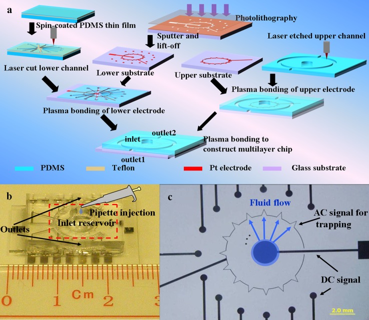
Figure 1a shows the fabrication process of a highly integrated microfluidic chip with 3D structures for particle manipulation. Compared with planar electrodes lying only on one substrate, the aligned electrodes on both top and bottom substrates is fabricated to realize 3D electrodes. The effective area for DEP effect is larger as it includes the whole channel height for top-bottom patterned electrode structures (3D electrode). However, for planar electrodes, it only holds a limited area near the surface of electrodes. The detailed information of the fabrication method can be found in our previous work.27 Here, we briefly describe fabrication of each of the layers and its assembly to form a 3D structured chip. The major steps of this fabrication include: patterning of electrodes, PDMS thin film preparation, laser cutting for lower channel and upper channel, and plasma bonding.
Figure 1.
Chip fabrication and real pictures. (a) Fabrication process flow of a 3D integrated microfluidic chip: the lower and upper channels as well as the chip are fabricated separately before being plasma bonded; (b) real image of fabricated microfluidic chip containing 13 channels in a small area; (c) optical microscope image of the electrodes configuration in the region indicated by red dashed square in 1(b). The arrowhead shaped electrode is designed for trapping particles by AC signal, while the circle shaped electrodes are used for manipulating particles by DC signal.
Standard photolithography, sputtering and lift-off process were processed to pattern planar electrodes on the glass substrate. The cleaned glass substrate was processed by spin-coating positive photoresist HPR 507 at a spin speed of 2000 rpm for 30 s, soft-baked on a hotplate at 110 °C for 2 min, UV exposed by Mask Aligner (ABM #2) for 20 s, and developed the photoresist using FHD-5 for 60 s, and post-baked on hotplate at 110 °C for 2 min. Cr/Pd electrodes (15 nm/150 nm thick) were deposited on this glass plate by a sputtering machine—Explorer 14 (Denton Vacuum). It was followed by a lift-off process to obtain microelectrodes patterned on glass plates.
PDMS thin film was spin coated on a substrate pretreated with Teflon (Dupont, Grade 601S1-100-1). The spin speed was set at 2000 rpm for 30 s and 3500 rpm for 30 s to get a uniform film with a thickness of 30 μm and 15 μm, respectively to process different particles with different dimensions. PDMS slab with a thickness of 2 mm was also prepared by mixing PDMS base and curing agent and pouring into a container.
After curing PDMS in an oven at 60 °C for 2 h, laser cutting of both PDMS thin film and PDMS slab were conducted by a CO2 laser plotter (Versa Laser System, Model VLS3.50, Universal Laser System, Ltd.). The cutting parameters were also optimized to get a smooth edge.28 The lower channel was directly cut with 0.5 W, at 0.75 mm/s, and 1000 pulse per inch (PPI), which produced a channel width around 200 μm, while the upper channel was etched with 2.5 W, at 0.75 mm/s, and 1000 pulse per inch (PPI), which created a channel of 900 μm by width and 500 μm by depth.
The bonding step was performed three times in the fabrication process. The first bonding step was conducted to bond PDMS thin film to glass substrate patterning with electrodes. The second bonding step was carried out to construct outlet on the upper layer of channel. The last bonding step was performed to bond the upper layer of electrodes to the patterned PDMS structure. The last bonding step is critical for fabrication since the metal patterns have to be aligned for constructing 3D electrodes. Both substrates were first activated in O2 plasma cleaner for 3 min, followed by transferring to microscope stage. Then the top and bottom substrates were manually aligned under the microscope. At last, bonding was performed by slowly moving two substrates together with well aligned electrodes. The closed microfluidic channel was formed to create a leak-tight channel at this stage.
Figure 1b shows the densely packed chip containing 13 channels in a 2 × 2 cm2 area demonstrating high-throughput capability of our device by exploiting our laser cutting technique. Compared to a traditional microdevice that comprises a single operating microchannel and a single outlet, our design with 13 individual microchannels arranged in the radial direction could operate in parallel and handle a larger volume of samples simultaneously. Figure 1c is the optical image of the bottom electrodes configuration in the region indicated by a red dashed square. The arrowhead electrode is used to apply AC signal for trapping, while the electrodes lay at two ends of microfluidic channel are used for imposing DC signal to generate electrophoretic and electroosmotic force. Our design takes the advantage of radial layout to arrange as many microchannels as we can to achieve fast processing of particle manipulation. By applying hydrodynamic, DC EO, and DC EP forces, no mechanical pump is needed. Instead, a simple pipette is enough for sample loading as shown in Figure 1b. After loading sample solution into the inlet reservoir, fluid will flow from the center to the ends in all these microchannels as shown in Figure 1c. Therefore, our device could be regarded as an integration of 13 microfluidic chip for sample preparation. In order to perform all experiments with low voltage power supplies, the channel depth is varied according to the relative DEP forces for different particles. Thus, the channel for trapping polystyrene particles was 30 μm in depth, while the channels for trapping yeast cells and E. coli are both 15 μm in depth. Inlet was defined by the big reservoir for sample loading and outlet was constructed by laser etching method at two sides of this chip.
Prior to each experiment, the chip was passivated by introducing 7% bovine serum albumin (BSA) solution for 2 h to prevent adhesion between the channel surface and bioparticles. Then, excess BSA was pumped out by introducing 10 mM NaCl solutions for five times. Due to the fact that the capillary force plays a significant role in the initial filling, microchannels were rinsed and filled with the same working solution by vacuum pump for total infiltration prior to performing particle manipulations.
RESULTS AND DISCUSSIONS
Characteristics of designed electrode
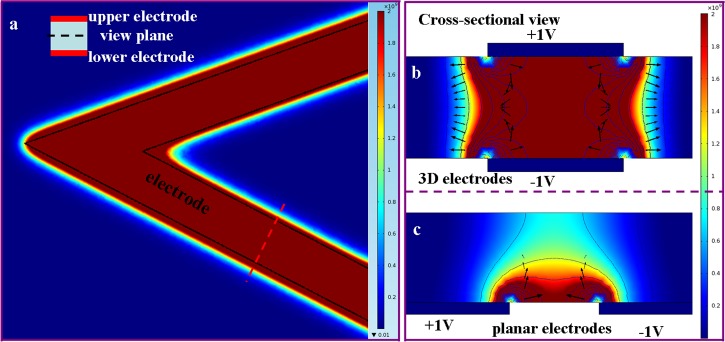
Electric field intensity is a key factor in determining DEP related phenomena. In order to demonstrate the advantage of our 3D electrode, finite element simulation was performed by using comsol 4.2 software. To determine the field intensity through the structure, a 3D model, electrostatics and stationary analysis were chosen. Geometry of the structure was defined using parameters of the fabricated chip. Parallel arrowhead-shaped electrodes on both the top and bottom surfaces with sandwiched 30 μm deep microchannels were constructed. The width of the electrodes was set to 40 μm. The view plane was set to the slice in the middle of the microchannel and parallel to the electrodes. The electric field intensity was plotted as square of electric field strength (). 3D simulation for this arrowhead geometry was performed for electric potential of upper and lower electrodes of +1 V and −1 V, respectively. Figure 2a gives the distribution of electric field intensity in the middle plane of the electrodes. The black lines represent the electrode edges. DEP force near the electrode region is directly related to the electric field gradient. We can see that field intensity is almost uniform in the region between two electrodes and it decays very fast near the edges resulting in a DEP force perpendicular to the electrode. Figure 2b shows the cross-sectional view of electric field intensity distribution and DEP force along the red dashed line in Figure 2a. It is seen that particles will experience strong DEP force along the entire channel. To outline benefits brought by 3D design in comparison to 2D design, we calculated the electric field intensity and DEP force of 2D planar electrode and gave the result in Figure 2c. DEP force was normalized by logarithm function with base of 10 to avoid large variation caused by the sharp corner. Owing to the symmetrical electrode configuration along channel depth, the electric field holds a much larger effective region for 3D electrodes compared with its counterpart—planar electrodes which generate DEP force only in a small area near the electrode and DEP force decreases rapidly away from the electrodes. In addition, particles will experience levitation force along the channel when they pass through the 2D planar electrodes, resulting in decrease of trapping efficiency.
Figure 2.
Simulation of electric field intensity and DEP force. (a) Electric field intensity distribution of arrowhead 3D electrode at the middle plane between upper electrode and lower electrode. The schematic diagram of 3D electrode is shown in the inset of (a). The potential was set to 1 V and −1 V for upper electrode and lower electrode, respectively. The red color represents high electric field, while the blue color represents low electric field. The black lines represent electrode edges; (b) cross-sectional view of field distribution and DEP force along the red dashed line in 2(a); (c) cross-sectional view of field distribution and DEP force of planar electrode located on one side of microchannel. The magnitude of DEP force was normalized by logarithm function with base of 10.
Compared to 2D planar electrode designs, the main advantages of this 3D electrode configuration include increase of trapping efficiency and reduction of Joule heating29, 30 and electrolysis. Indeed, for planar electrodes, a high electric field has to be applied to balance hydrodynamic force experienced by particles, which results in severe Joule heating coming from the reaction of ions under electric field. Therefore, our 3D configuration is preferred for dielectrophoretic applications.
Particles and cells choice
Particles respond differently to various forces depending on their sizes, geometries, structures and content. In this study, we selected three types of particles/cells of different properties, namely, polystyrene particles (10 μm in diameter), yeast cells (4–5 μm in diameter), and E. coli (0.5 μm × 2 μm). Eukaryotic yeast cell's structure is different from that of prokaryotic E. coli, and thus, responds differently to the electric field and its gradient.
Trapping of PS particles
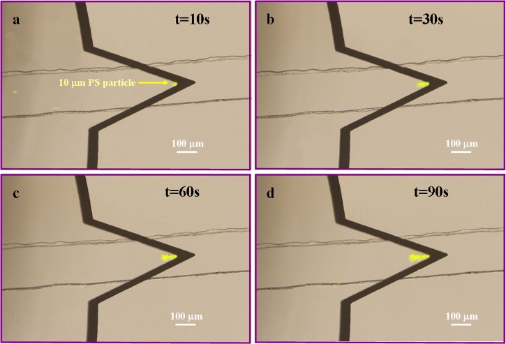
The capability of this technique was first demonstrated by trapping 10 μm fluorescent PS particles. Correspondingly, the chip was designed with a channel depth of 30 μm and maximum height of 2 mm between inlet and outlet reservoirs. Buffer solution with the same ion concentration as sample solution was first used to infiltrate microfluidic channels. Then, 20 μl sample solution containing 10 μm fluorescent PS particles was introduced into the inlet reservoir with a pipette. An AC voltage of 21 Vpp and frequency of 50 kHz was applied between the upper electrode and lower electrode, corresponding to maximum field strength of 7 × 10⁶ V/m between two electrodes. Figure 3 illustrates the fast accumulation of particles by nDEP as time went by in a single channel. It is seen that the number of particles trapped at the tip of arrowhead-shaped microelectrode is increased from t = 10 s (Figure 3a) to t = 90 s (Figure 3d).
Figure 3.
Accumulation of 10 μm PS particles by applying AC signal of 21 Vpp at 50 kHz with field strength of 7 × 10⁶ V/m on the arrowhead electrode. (a) t = 10 s; (b) t = 30 s; (c) t = 60 s; (d) t = 90 s. The channel depth was 30 μm.
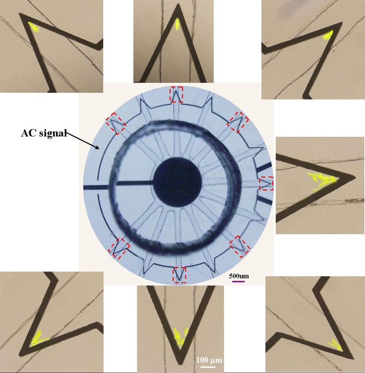
After 90 s of particle trapping, optical images of individual trapping regions were taken and some of them are shown in Figure 4, giving the experimental demonstration of the parallel operation of the different channels in our chip. The central picture is the full view of the chip containing 13 channels in total. These channels can function together to trap particles, thus the processing time can be largely reduced compared with a single channel. The radial design of channel layout was in favor of sample solution loading. The vertices were indicated by red dashed squares. Fluorescent PS particles were trapped at the tips of electrodes, where the gradient of electric field reaches its maximum value. It is noted that the amplitude of AC signal varies according to the velocity driving by the height difference of solution in inlet and outlet reservoirs. A higher voltage was applied in this case to ensure that all particles are trapped when they travel at the maximum velocity.
Figure 4.
Optical images of the whole trapping region containing 13 channels in total and several individual channels indicated by red dashed squares. It shows that every channel could be used for trapping particles.
Collection and release of yeast cells
Trapping of bioparticles was first demonstrated by collection of yeast cells in our chip with channel depth of 15 μm. Trapping of cells is important for a variety of applications including drug testing, toxicology, and basic cell biology. Yeast cells experienced negative DEP (n-DEP) in a buffer solution with conductivity of 140 μS/cm at 50 kHz according to the relative complex permittivities of cells and medium, which determines the CM factor. 20 μl yeast suspensions was introduced into the inlet reservoir using a pipette. To study the minimal necessary input voltage in view of future portable diagnostic kit, during the collection process, the AC driving signal was increased from 0 to 15 V peak-to-peak voltage with a fixed frequency of 50 kHz. It was found that 10 Vpp AC signal at frequency of 50 kHz was enough to trap almost all cells in the channel. When the signal was imposed on the electrodes, cells began to stop near the vertices of the inner electrodes, where the electric field gradient is the highest.
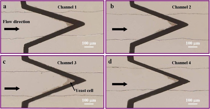
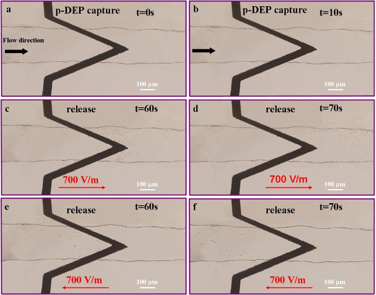
Collection of yeast cells by negative DEP was shown in Figure 5, where pictures taken after running the device for 2 min were presented for 4 different channels. To analog different conditions faced in pathogen detection, we tested our approach to deal with media of low conductivities in which yeast cells exhibit positive DEP (i.e., 2 μS/cm in our experiment). In order to demonstrate the whole process of manipulation of yeast cells, AC and DC signals were applied to trap and release cells, respectively. The method comprises two steps: (1) yeast cells were isolated from sample solution and trapped between upper and lower electrodes by positive DEP (p-DEP) when AC electric field was applied; and (2) yeast cells were released by combined EP and EO forces, when DC electric field was applied. Figure 6 shows the pre-concentration and release of yeast cells. Yeast cells were first suspended in a solution having lower conductivity—0.28 mM NaCl solution (2 μS/cm), followed by loading 10 μl sample solutions into the inlet reservoir. When 5 Vpp signal at 50 kHz was applied between the upper and lower electrodes, yeast cells tend to aggregate at the highest electric field region since yeast cells were more polarizable than the medium (positive DEP). Figures 6a, 6b are two snapshot pictures taken at t = 0 s and t = 10 s, respectively. We can see that the entire channel region was divided into two sub-domains by electrodes: the one on the left distributes cells, while the other one does not.
Figure 5.
Trapping of yeast cells in four channels to demonstrate the capability of pre-concentration of bioparticles by the proposed device. Pictures were taken after applying a trapping signal for 2 min. The applied AC signal was 10 Vpp at 50 kHz and the channel height was 15 μm. The medium conductivity was adjusted to 140 μS/cm for collection of yeast cells by negative DEP.
Figure 6.
Capture and release of yeast cells. (a), (b) Capture of yeast cell by positive DEP at medium conductivity of 2 μS/cm. Yeast cells were collected between upper electrode and lower electrode where the electric field strength was highest. Flow was driving by difference of water level between inlet and outlet. The applied AC signal was 5 Vpp at 50 kHz and the channel height was 15 μm. (c)–(f) Release of yeast cells by applying DC field of 700 V/m after collection of yeast cells for 55 s. These figures demonstrated that yeast cells travelled in the same direction as the electric field.
After collecting yeast cells for 55 s, the solutions in inlet and outlet were at the same level and there was no hydrodynamic force in the channels. Then AC signal was turned off and DC electric field in the direction from inlet to outlet was applied. Due to electrophoretic force and electroosmotic force under an electric field of 700 V/m, yeast cells were moving towards outlet (Figures 6c, 6d). Electric field also assisted to direct cells back to inlet reservoir by switching the direction of field from outlet to inlet, as can be seen in Figures 6e, 6f. After moving to outlet or inlet, yeast cells could be collected by a pipette at a much higher concentration for further analysis.
E. coli capture
Detection of pathogens is prerequisite precursor in prevention and diagnosis of infectious diseases, drug discovery, clinical research, biological warfare, as well as food safety administration.31E. coli is a type of bacteria that naturally occur in the intestinal tracts of human and warm-blooded animals to produce vitamins, but one particular pathogenic strain, E. coli O157:H7, produces toxins that damage the lining of the intestine, causing gastroenteritis, anemia and serious complications such as hemolytic uremic syndrome (HUS) and thrombotic thrombocytopenic purpura (TTP).32 The detection and identification of foodborne pathogens and other contaminants in raw food materials in processing and assembly lines, ports of entry and drinking water supplies and hospitals, largely rely on conventional culturing techniques. The limitations of culturing are costly, time-consuming, and require bulky equipments, making them unsuitable for on-site pathogen detection and analysis. By comparison, a field-deployable biosensor is easy to use, portable, reagent free, and fast.
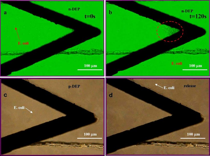
E. coli are difficult to collect due to their small size and relatively small DEP force. 3D electrode configuration may be a suitable approach for E. coli collection. Indeed, as discussed in the simulation part, our 3D design allows to generate a high electric field in the whole region along the height of channel. Here, we demonstrate the capture of E. coli by both n-DEP and p-DEP. 10 μl sample solution was firstly loaded into the inlet reservoir for trapping E. coli. NaCl concentration was adjusted to 53.2 mM (380 μS/cm) for n-DEP trapping and 0.28 mM (2 μS/cm) for p-DEP trapping. The applied AC signal was 15 Vpp at 50 kHz and 10 Vpp at 50 kHz for n-DEP and p-DEP, respectively. And the channel depth was 15 μm. Figures 7a, 7b with green background showed that E. coli coming from the left part of channel were trapped by AC n-DEP at the location where the electric field gradient was largest, while Figures 7c, 7d with brown background depicted the p-DEP trapping (7c) and release (7d) of E. coli. The applied DC field for releasing was 700 V/m.
Figure 7.
Collection and release of E. coli. (a), (b) Collection of E. coli by negative DEP at medium conductivity of 380 μS/cm at t = 0 s and t = 120 s, respectively. AC signal of 15 Vpp at 50 kHz was applied in the channel of 15 μm in depth; (c), (d) Collection of E. coli by positive DEP at medium conductivity of 2 μS/cm and release of E. coli after trapping for 1 min. E. coli bacteria were collected between upper electrode and lower electrode in 8c. The applied AC signal was 10 Vpp at 50 kHz and the channel height was 15 μm. The applied DC field for releasing was 700 V/m.
Separation of live and dead yeast cells
Sorting of different kinds of microparticles is often necessary prior to sample analysis. Separating live and dead cells is much more difficult due to their similarities in content and dimensions. This process is critical at an early diagnostic stage for efficient drug screening.33 These tests also evaluate the effectiveness of a pesticide or insecticide, or assess environmental damage due to toxins.
In order to characterize the DEP response of live and dead yeast cells under AC electric field, numerical calculation of real part of the Clausius-Mossotti (CM) factor was performed by fortran (Compaq visual fortran 6). The CM factor is determined by
| (4) |
where and represent the complex permittivities of particle and medium and the complex permittivity is defined as , in which , σ is the electric conductivity and ω is the angular frequency of the applied electric field.
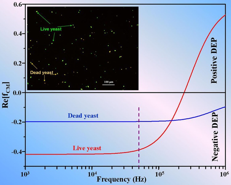
A three shell model of cell wall, cytoplasm, and cell nucleus developed by Huang et al.34 was adopted for calculating the CM factor. The geometrical and electrical properties of yeast cell were taken from the literature.35 Briefly, the following properties of live and dead yeast cells were used, based on Levpiriyamony's optimized data: radii of 2.5 μm for wall, 2.36 μm for cytoplasm, and 2.35 μm for nucleus; with conductivities of 140 μS/cm for wall of live cell, 15 μS/cm for wall of dead cell, 0.0025 μS/cm for cytoplasm of live cell, 1.6 μS/cm for cytoplasm of dead cell, 2000 μS/cm for nucleus of live cell, 140 μS/cm for nucleus of dead cell; and relative permittivity of 60 for wall, 6 for cytoplasm, 50 for nucleus of live cell, 78 for nucleus of dead cell. The conductivity and permittivity of the medium were set to 140 μS/cm and 78, respectively. Figure 8 depicted the real part of the CM factor of live yeast cell (red) and dead yeast cell (blue) corresponding to different applied frequencies of AC signal. The upper part of this graph above the transverse line (Re (fCM) = 0) indicated positive CM factor resulting in positive DEP force, while the lower part indicated negative CM factor resulting in negative DEP force. The violet dashed line represented the working frequency for separation. The inset in this figure was an optical image of live and dead yeast cells after staining by fluorescent dyes described in previous sample preparation part. We can see that live yeast cells are marked with green, while dead yeast cells tend to exhibit orange color. This figure shows the difference of real part of the CM factor at the working frequency of 50 kHz, giving rise to different DEP force which is proportional to real part of the CM factor.
Figure 8.
The real part of CM factor as a function of electric field frequency for live (red line) and dead (blue line) yeast cells at medium conductivity of 140 μS/cm. Positive value of real part of CM factor represents yeast cells under positive DEP, while the negative value represents cells under negative DEP. The violet dashed line indicates the working frequency for separating them due to the difference in DEP forces. The inset is the optical microscope image of mixture of live and dead yeast cells dyed by two colors.
The electrophoretic force is identical for live and dead cells,36 which imply that a DC signal cannot be used to separate live and dead cells. However, complex permittivity depends on cell's viability and thus corresponds to different dielectrophoretic forces. Therefore, DEP could be applied to separate cells according to their vitality. Here, both DC and AC signals were applied for separation by taking the advantage of identical DC electrophoretic, electroosmotic forces, and different AC dielectrophoretic force.
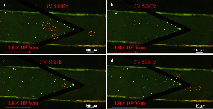
To separate cells, we punched a hole at the channel end to place Platinum (Pt) wires. Pt wires were introduced here to replace existing planar electrodes because they allow to generate almost uniform electric field along the channel height. The water level of inlet and outlet were first set to be the same. Then 20 μl buffer solution without cells was loaded in the outlet reservoir, which is followed by the injection of 15 μl yeast suspensions with live and dead cells in the inlet reservoir. After the water had reached the same level again, DC signal with the electric field strength of 1.0 × 10³ V/m was applied and AC signal with frequency of 50 kHz at which both live cells and dead cells experienced negative DEP was imposed on the upper electrode and lower electrode. When cells passed through the converged electrodes, amplitude of AC signal was adjusted from 0 V to 10 V. It was found that 3 Vpp was suitable to separate them under the apparent cell velocity of ∼15 μm/s. Figure 9 shows the separation process with time interval of 5 s. We can see that live yeast cells experienced large negative DEP force and they were trapped at the edge of converged electrodes as predicted in Figure 8. On the other hand, dead yeast cells were prone to travel towards the outlets. In order to do statistics analysis of separation efficiency, cells in the outlet were counted under fluorescent microscope. Ideally, there should be only dead cells in the outlet reservoir. Therefore, the separation efficiency was obtained from the division of the number of live cells to the total number of yeast cells. The efficiency was larger than 90% after conducting separation by this platform.
Figure 9.
The separation process of live and dead yeast cells with time interval of 5 s. The applied AC signal was 3 Vpp at 50 kHz and electric field was 1.0 × 10³ V/m. The channel height is 30 μm. Live yeast cells experienced large DEP force were trapped at the tip of arrowhead electrode, while dead yeast cells moved towards the outlet under electrokinetic force. Some dead yeast cells are highlighted by orange dashed circles for a better view.
CONCLUSIONS AND PERSPECTIVES
In this paper, we have proposed a new technique combining hydrodynamic, electroosmotic, electrophoretic, and dielectrophoretic forces for microparticle manipulation in microchannels. In this technique, hydrodynamic force was used to generate fluid flow, DEP force was applied to trap particles and combined EO and EP forces were employed to redirect and release particles. Parameters such as pressure inside microchannels, DEP, EO, and EP forces in this densely packed microfluidic device are adjustable according to the properties of different sample matrices. The ability of this technique to distinguish electrokinetic force from dielectrophoretic force enables convenient tuning to isolate different targeted particles. The success of our technique relies in ingenious chip design to integrate these different forces and operates on a same chip. Taking advantage of a 3D design and fabrication process, we could perform good optimization of different forces, and possibly lowering applied voltage.
Our system was successfully tested with particles and cells of properties representative of common colloidal and biological samples disparity that may contain many components. Although the medium conductivity in the demonstrated experiment was low (<400 μS/cm), several method could be used to extend applications of this platform to high conductivity media. Such as: reduction of the sample solution velocity, increase the working frequency, as well as binding target small particles to large particles experiencing large DEP force. We also tested sorting of yeast cells with different vitalities, showing the good discrimination between microparticles having close properties. All experiments were conducted with a simple pipette for sample loading. This “pump-free” aspect is of foremost importance as it means our device may be used by non-initiated user, for instance, for self diagnosis or on site analysis, by simply introducing a droplet of the sample of interest. We have thus proven that this technique has the potential in applying in particle manipulation to serve as pathogen detector and analyzer, as well as sample preparation for further analysis. Our present chip integrates trapping, release, and sorting of particles in a single chip. Considering some real applications in diagnosis, other modules may be further integrated on the same chip to perform sensing and fluid steering operation.
ACKNOWLEDGMENTS
The authors acknowledge the financial support provided by the Hong Kong Research Grants Council Grant No. HKUST604710, 605411. This publication was based on work partially supported by Award No. SA-C0040/UK-C0016 made by King Abdullah University of Science and Technology (KAUST).
References
- Velev O. D. and Bhatt K. H., Soft Matter 2, 738 (2006). 10.1039/b605052b [DOI] [PubMed] [Google Scholar]
- Linder V., Analyst 132, 1186 (2007). 10.1039/b706347d [DOI] [PubMed] [Google Scholar]
- Weigl B., Domingo G., LaBarre P., and Gerlach J., Lab Chip 8, 1999 (2008). 10.1039/b811314a [DOI] [PMC free article] [PubMed] [Google Scholar]
- Chin C. D., Linder V., and Sia S. K., Lab Chip 7, 41 (2007). 10.1039/b611455e [DOI] [PubMed] [Google Scholar]
- Noeth N., Keller S., Fetz S., Geschke O., and Boisen A., in Proceedings of the Solid-State Sensors, Actuators and Microsystems Conference (Transducers), Denver, CO (IEEE, 2009), p. 2034.
- Chen X., Cui D., Liu C., Li H., and Chen J., Anal. Chim. Acta 584, 237 (2007). 10.1016/j.aca.2006.11.057 [DOI] [PubMed] [Google Scholar]
- Cheng I.-F., Chang H., Hou D., and Chang H., Biomicrofluidics 1, 021503-1 (2007). 10.1063/1.2723669 [DOI] [Google Scholar]
- Li S., Li M., Hui Y. S., Cao W., Li W., and Wen W., Microfluid. Nanofluid. 14, 499 (2013). 10.1007/s10404-012-1068-6 [DOI] [Google Scholar]
- Pethig R., Biomicrofluidics 4, 022811-1 (2010). 10.1063/1.3456626 [DOI] [PMC free article] [PubMed] [Google Scholar]
- Gangwal S., Pawar A., Kretzschmar I., and Velev O. D., Soft Matter 6, 1413 (2010). 10.1039/b925713f [DOI] [Google Scholar]
- Honegger T. and Peyrade D., Biomicrofluidics 6, 044115 (2012). 10.1063/1.4771544 [DOI] [PMC free article] [PubMed] [Google Scholar]
- Juárez J. J., Feicht S. E., and Bevan M. A., Soft Matter 8, 94 (2012). 10.1039/c1sm06414b [DOI] [Google Scholar]
- Bogunovic L., Eichhorn R., Regtmeier J., Anselmetti D., and Reimann P., Soft Matter 8, 3900 (2012). 10.1039/c2sm07053g [DOI] [Google Scholar]
- Gordon J. E., Gagnon Z., and Chang H.-C., Biomicrofluidics 1, 044102-1 (2007). 10.1063/1.2818767 [DOI] [PMC free article] [PubMed] [Google Scholar]
- Pysher M. D. and Hayes M. A., Anal. Chem. 79, 4552 (2007). 10.1021/ac070534j [DOI] [PubMed] [Google Scholar]
- Zhu J. and Xuan X., Biomicrofluidics 5, 024111 (2011). 10.1063/1.3599883 [DOI] [PMC free article] [PubMed] [Google Scholar]
- Gao J., Sin M. L. Y., T., Liu, Gau V., Liao J. C., and Wong P. K., Lab Chip 11, 1770 (2011). 10.1039/c1lc20054b [DOI] [PMC free article] [PubMed] [Google Scholar]
- Liao K.-T., Tsegaye M., Chaurey V., Chou C.-F., and Swami N. S., Electrophoresis 33, 1958 (2012). 10.1002/elps.201100707 [DOI] [PubMed] [Google Scholar]
- Zeng S., Chen C.-H., Mikkelsen J. C., and Santiago J. G., Sens. Actuators B 79, 107 (2001). 10.1016/S0925-4005(01)00855-3 [DOI] [Google Scholar]
- Wu J., Ben Y., Battigelli D., and Chang H., Ind. Eng. Chem. Res. 44, 2815 (2005). 10.1021/ie049417u [DOI] [Google Scholar]
- Dutta D. and Ramsey J. M., Lab Chip 11, 3081 (2011). 10.1039/c1lc20329k [DOI] [PubMed] [Google Scholar]
- Judy J., Maynes D., and Webb B. W., Int. J. Heat Mass Transfer 45, 3477 (2002). 10.1016/S0017-9310(02)00076-5 [DOI] [Google Scholar]
- Li M., Li S., Cao W., Li W., Wen W., and Alici G., J. Micromech. Microeng. 22, 095001 (2012). 10.1088/0960-1317/22/9/095001 [DOI] [Google Scholar]
- Jones T. B., Electromechanics of Particles (Cambridge University Press, Cambridge, UK, 1995). [Google Scholar]
- Li H. and Bashir R., Sens. Actuators B 86, 215 (2002). 10.1016/S0925-4005(02)00172-7 [DOI] [Google Scholar]
- Keymer J. E., Galajda P., Lambert G., Liao D., and Austin R. H., Proc. Natl. Acad. Sci. U.S.A. 105, 20269 (2008). 10.1073/pnas.0810792105 [DOI] [PMC free article] [PubMed] [Google Scholar]
- Li M., Li S., Wu J., Wen W., Li W., and Alici G., Microfluid. Nanofluid. 12, 751 (2012). 10.1007/s10404-011-0917-z [DOI] [Google Scholar]
- Wang L., Kodzius R., Yi X., Li S., Hui Y. S., and Wen W., Sens. Actuators B 168, 214 (2012). 10.1016/j.snb.2012.04.011 [DOI] [Google Scholar]
- Moulton T. and Ananthasuresh G. K., Sens. Actuators, A 90, 38 (2001). 10.1016/S0924-4247(00)00563-X [DOI] [Google Scholar]
- Zhu J., Sridharan S., Hu G., and Xuan X., J. Micromech. Microeng. 22, 075011 (2012). 10.1088/0960-1317/22/7/075011 [DOI] [Google Scholar]
- Foudeh A. M., Didar T. F., Veresab T., and Tabrizian M., Lab Chip 12, 3249 (2012). 10.1039/c2lc40630f [DOI] [PubMed] [Google Scholar]
- Doyle M. P., Beuchat L. R., and Montville T. J., Food Microbiology: Fundamentals and Frontiers (American Society for Microbiology (ASM), Washington, DC, 1997). [Google Scholar]
- Patel S., Showers D., Vedantam P., Tzeng T., Qian S., and Xuan X., Biomicrofluidics 6, 034102 (2012). 10.1063/1.4732800 [DOI] [PMC free article] [PubMed] [Google Scholar]
- Huang Y., Holzel R., Pethig R., and Wang X. B., Phys. Med. Biol. 37, 1499 (1992). 10.1088/0031-9155/37/7/003 [DOI] [PubMed] [Google Scholar]
- Lewpiriyawong N., Kandaswamy K., Yang C., Ivanov V., and Stocker R., Anal. Chem. 83, 9579 (2011). 10.1021/ac202137y [DOI] [PubMed] [Google Scholar]
- Lapizco-Encinas B. H., Simmons B. A., Cummings E. B., and Fintschenko Y., Anal. Chem. 76, 1571 (2004). 10.1021/ac034804j [DOI] [PubMed] [Google Scholar]


