Abstract
Lab-on-a-chip systems have been rapidly emerging to pave the way toward ultra-compact, efficient, mass producible and cost-effective biomedical research and diagnostic tools. Although such microfluidic and micro electromechanical systems achieved high levels of integration, and are capable of performing various important tasks on the same chip, such as cell culturing, sorting and staining, they still rely on conventional microscopes for their imaging needs. Recently several alternative on-chip optical imaging techniques have been introduced, which have the potential to substitute conventional microscopes for various lab-on-a-chip applications. Here we present a critical review of these recently emerging on-chip biomedical imaging modalities, including contact shadow imaging, lensfree holographic microscopy, fluorescent on-chip microscopy and lensfree optical tomography.
Index Terms: on-chip imaging, on-chip microscopy, lensfree imaging, lensless microscopy, shadow imaging, lensfree holography, computational biomedical imaging
I. INTRODUCTION
Though it was invented more than 400 years ago, the optical microscope is still the leading visualization tool and one of the gold standards for biological and biomedical analysis. Several microscopy modalities emerged during the past century, and even if we limit ourselves to the visible portion of the electromagnetic spectrum we find numerous techniques such as fluorescence microscopy, differential interference contrast microscopy, phase contrast microscopy, dark field microscopy, confocal microscopy, etc. In the last two decades, these methods became even more powerful with the introduction of super-resolution techniques to break the diffraction limit of conventional microscopy systems.
In parallel to the evolution of optical microscopy, lab-on-a-chip systems and microfluidics also emerged as powerful fields, creating new opportunities for sample preparation and processing on a chip [1]. During the last decade various important tasks had been miniaturized with the use of these lab-on-a-chip concepts, including cell and tissue culturing [2–4], cell separation and sorting [5], [6], cell lysis [7], DNA and RNA amplification (Polymerase Chain Reaction) [8], fluorescent labeling [9], analytical techniques for micro-arrays [10], and sensing [11]. One of the goals of these systems is to create cost-effective and compact diagnostic tools for biomedical use. Although most of these lab-on-a-chip systems achieved high levels of integration, imaging of these on-chip platforms is still usually done with bulky conventional microscopy systems, which might partially limit their potential impact, especially for point-of-care and field applications.
In the last few years, however, various compact on-chip imaging approaches have been emerging to potentially replace conventional lens-based microscopes for lab-on-a-chip applications. Here, we present a critical review of these new on-chip imaging modalities also covering possible biomedical applications. For this end, in Section II we give an introduction to lensfree in-line holographic microscopy. Section II.A details lensless digital holographic microscopy which uses coherent spherical wavefront illumination. Section II.B discusses some of the recent partially-coherent lensfree digital holographic microscopy methods using plane wave illumination. We then review non-holographic on-chip transmission imaging systems in Section III. Section IV reviews some of the existing lensless optical tomography approaches, while Section V gives a short overview of the current capabilities of on-chip fluorescent microscopes. We conclude our review with future prospects of such lensless on chip imaging modalities.
II. Lensfree Digital Holographic Microscopy
Lensless imaging for microscopy can be dated back to 1948 when Dennis Gabor first proposed his new microscopic imaging principle for electron microscopy to get rid of the imperfect magnetic lenses [12]. His idea, to capture the interference of the illuminating wave, i.e., the reference wave, and the waves diffracted by the object, or the object waves, on a photographic plate marked the birth of holography (see Figure 1).
Fig. 1.
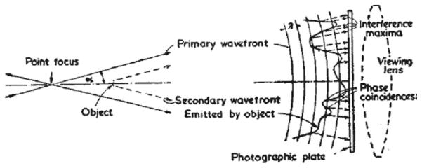
Gabor’s original holography geometry. Reprinted by permission from Macmillan Publishers Ltd: Nature [12], copyright (1948).
Holography is a two-step process, i.e., image capture and reconstruction. In the first step (recording), the amplitude and the phase information of the object wave is captured as an interference pattern. In an in-line holographic setup the illumination constitutes as the reference wave, R(x,y,z), under the assumption that the density of objects is not exceedingly large, thus the major part of the illuminating beam remains unscattered, as if not having interacted with the objects. However, a relatively smaller portion of the illuminating light is scattered by the sample, constituting the object wave, O(x,y,z). The degree of coherence (both temporal and spatial) of the illumination at the sensor plane should be sufficient to permit the reference and object waves to superpose in complex amplitudes, giving rise to a measured interference pattern, i.e., the hologram:
| (1) |
In Eq. (1), the first term is ideally a uniform background signal, which does not contain useful information regarding the objects. The second term is a self-interference term, corresponding to the intensity of the diffracted wave at the sensor plane. This term has a relatively low intensity, compared to the last two terms, and can be neglected for weakly scattering samples. The last two terms are the dominant holographic terms of interest since we typically have: |R| > |0|. In traditional ‘analog’ holography, when the recording material is illuminated by this interference pattern, and later developed, its’ transmittance (t) becomes proportional to the recorded intensity, thus:
| (2) |
where k is just a proportionality constant. To obtain the original image of the object from the recorded hologram a second step, i.e., the hologram reconstruction, is needed, which was traditionally achieved by illuminating the recording medium with the same reference wave. The wave diffracted by this medium can be expressed as:
| (3) |
Ignoring the first term since it constitutes a uniform background, the dominant terms in Eq. (3) are the third and fourth terms, which are proportional to the original object wave and its complex conjugate, respectively. The latter is also referred to as the conjugate object wave, which has a reverse curvature compared to the object wave, and is therefore responsible for the twin image artifact in in-line holographic imaging architectures - a topic that we will revisit when we discuss the numerical details of image reconstruction.
Different than analog systems, in digital holography the hologram recording is done by an electronic image sensor-array, while the reconstruction step is done numerically using a digital processor, by virtually illuminating the recorded holographic pattern with the reference wave, and then using various wave propagation algorithms to calculate the complex field distribution at the object plane, which ideally yields the digital image (both phase and amplitude) of the object itself.
The use of an electronic image sensor-array instead of a photographic plate, and the digital reconstruction of the captured hologram using a computer, was first demonstrated by J. W. Goodman and R. W. Lawrence in 1967 [13]. But only with the use of modern digital image sensors for hologram recording, demonstrated by e.g., U. Schnars and W. Jüptner [14] in 1994, was digital holography truly born, yielding rather competitive images.
To be able to efficiently simulate the effect of the reference wave, one has to know the exact phase distribution of illumination light. Since measuring the phase distribution of an arbitrary wave with the necessary precision is problematic, digital holography uses sources with known, and numerically easy-to-represent, wavefronts for illumination, such as spherical or planar wavefronts. Both of these approaches are used in lensless holographic microscopy, but their capabilities and the required reconstruction methods are different.
The wave propagation algorithms used to reconstruct the digital holograms are based on the scalar diffraction theory and are the numerical solutions of either the Fresnel-Kirchhoff, or the Rayleigh-Sommerfeld diffraction integrals. As with any numerical method there is a natural trade-off between the complexity and the accuracy of the calculations. The most commonly used digital reconstruction algorithm is based on the Fresnel propagation method [15]:
| (4) |
where E1 is the scalar electric field in the hologram plane, E2 is the scalar electric field in the object plane, x and y represent the Cartesian coordinates of the corresponding planes perpendicular to the optical axis, z is the propagation distance, and λ is the wavelength of the illumination. Equation (4) can be calculated using a single FFT [16], but as its name suggests it uses the Fresnel approximation, making it only valid for relatively low numerical aperture (NA) systems, thus it offers only limited resolution.
One of the most accurate methods for wave propagation is the calculation of the Rayleigh-Sommerfeld diffraction integral without any approximations, using the angular spectrum method [17]:
| (5) |
where
| (6) |
The integral can be rewritten into the form of a convolution using a propagation kernel h(x,y,z):
| (7) |
| (8) |
where . Using the convolution theorem one can write:
| (9) |
| (10) |
| (11) |
Here, fx, fy and fz are the corresponding Fourier frequencies for x, y, and z, respectively.
Using the above described angular spectrum method for wave propagation, the Rayleigh-Sommerfeld diffraction integral can be calculated numerically by determining the propagation kernel, using a digital a low pass spatial filter, which blocks spatial frequencies corresponding to the evanescent waves, and performing two FFTs. Though theoretically more accurate, the angular spectrum method was initially less popular, since it requires special care to avoid spatial sampling problems of the transfer function, which can possibly result in severe numerical errors as the propagation distance increases. This problem was later solved by Matsushima, by limiting the bandwidth of the propagation [18].
During the reconstruction of in-line holograms the object wave and the conjugate object wave represent optical fields traveling in opposite directions. As a result, upon propagation of the recorded hologram toward the object plane, one of these terms converges to an image of the object, while the other further diverges, forming a weaker defocused twin-image related artifact that is concentric with the actual image. This spatial artifact is one of the main drawbacks of in-line digital holographic imaging systems, and is caused by the fact that the image sensor only measures the intensity of the light, and thus, the phase of the scalar electric field at the hologram plane is lost. Phase retrieval algorithms [19] make use of the square-root of the hologram intensity (i.e., the amplitude) as a starting point to guess the optical field at the sensor plane. This initial phase guess (which can start with e.g., a random guess) is then refined by iteratively updating the phase as the field is propagated back-and-forth between the measured hologram plane and the reconstructed object plane, while the size and shape of the objects (i.e. an object support) is used as a constraint in these iterations. This method, however, is sensitive to the accuracy of the used object support. Another approach to retrieve the phase information is to capture two or more holograms of the same object at different heights/distances, and iteratively propagate between these different hologram planes while continuously adjusting the phase of the wavefront until the amplitude of each height matches the measured holograms [20], [21]. This method has the advantage to work without the need for any object support, thus making it more suitable for imaging of dense objects.
There is another elegant optical solution for the above discussed twin image problem, which also overcomes the object density related issues. In an off-axis holography setup, a beam splitter is used to split the illuminating beam into two paths before it reaches the sample. One of these beams propagates through the optical system undisturbed by the object creating an external reference wave. This reference wave reaches the detector plane under a small angle compared to the object wave, hence the name off-axis holography. Despite its advantages for handling twin-image artifacts, this off-axis imaging architecture suffers from reduced field-of-view (FOV) and effectively a reduced space bandwidth product. Nevertheless, this technique is a frequently used method in digital holographic microscopy [22], [23], but in this review we will rather focus on in-line holographic architectures, where no external reference wave is used, leading the way to easier to align and operate field-portable microscopes with wide FOV. We should note here that compact and field-portable off-axis imaging systems have also been recently demonstrated [24], [25].
A. Digital in-line holographic microscopy with coherent spherical wavefront illumination
A powerful application of Gabor’s idea for digital holographic optical microscopy was presented by Kreuzer Group [26], [27]. By using a pinhole with a size smaller than 1.22*λ, where λ is the wavelength of the illumination, a near-perfect spherical wavefront can be created. This spherical wavefront is then used to illuminate the target/object whose distance from the aperture (z1) is much smaller than its distance from the sensor (z2) as shown in Fig. 2.
Fig. 2.
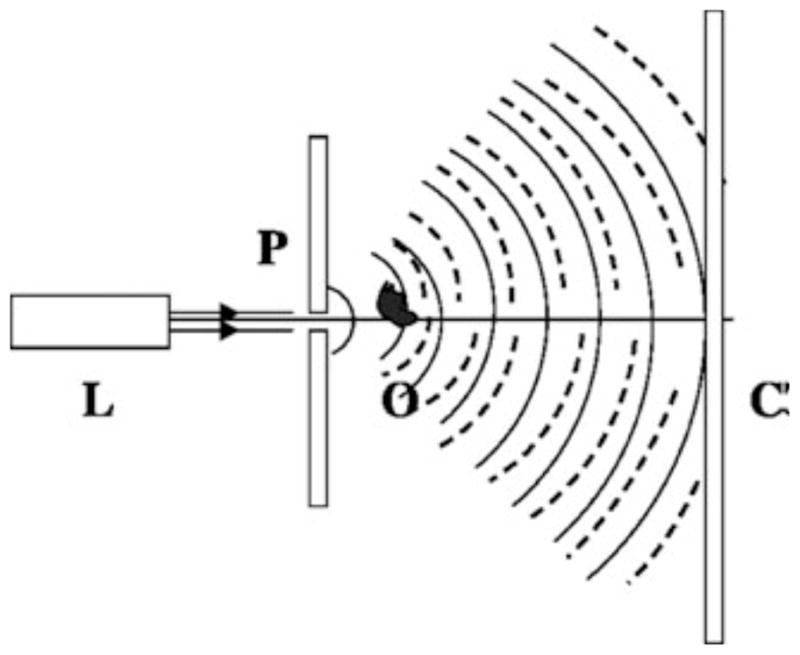
Sketch of a digital in-line holographic microscope. A laser (L) is focused onto a submicron pinhole (P) so that the emerging wave illuminating the object (O) is spherical. The resulting interference pattern or hologram is recorded on the screen (C) with a typical fringe magnification of ~10–35. The solid and dashed lines represent the reference wave and the scattered object wave, respectively. Reprinted from [27] with permission from OSA.
As described before, the scattered object wave interferes with the illumination beam at the sensor plane and this interference pattern is captured by the image sensor. The use of this optical setup (Figure 2) leads to a fringe magnification in the system: M = 1+z2/z1, which typically is around 10–35. The achievable FOV of lensless digital holographic systems is proportional to the active area of the image sensor chip and is inversely proportional to the square of the fringe magnification term (M). Since the fringe magnification term helps to overcome the sampling limit introduced by the pixel-size (px) of the used sensor chip, the spatial resolution (δx) of this type of imaging architecture is mainly limited by the width of the image sensor chip (W), i.e., δx = λ/2NA = λz2/W.
Initially, digital reconstruction algorithms employed in this architecture had difficulty of dealing with spatial sampling of a spherical reference wavefront at the sensor plane for high numerical apertures. An important solution to this problem in order to reconstruct high NA holograms is based on the Kirchhoff-Fresnel transform, and was first proposed for photoelectron holography by Barton [28], and later improved by Kreuzer Group [26], [29] by adding a spherical coordinate transformation step to the reconstruction method. This approach solves the Fresnel-Kirchhoff diffraction integral with the approximation that the position of the object is closer to the light source than to the sensor. It typically employs two recording steps, first recording the reference spherical wave without the object, and second, recording the hologram of the object. The difference of the two captured intensity patterns exhibits several advantages and helps digital removal of any possible imperfections resulting from the illumination or the sensor-array. This numerical reconstruction method is capable of reconstructing images of biological specimen with sub-micron resolution [30]. Recently Kanka et al. also reported another reconstruction scheme which solved the aliasing problem of the spherical reference wave, enabling the use of the more rigorous angular spectrum method [31]. A computationally more efficient version of this algorithm [32] was recently demonstrated to reconstruct holograms with an NA of ~0.8. As an example, using a modulated laser with reduced coherence length can resolve a cluster of e.g., 816 nm microbeads (see Fig. 3) [33].
Fig. 3.
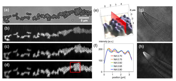
(a) Microscope image (0.75 NA) of 816nm PMMA beads. (b) DIHM image reconstructions of the same area using a highly coherent laser and (c) a partially coherent laser. (d) DIHM image reconstruction with an additional numerical correction of the glass sample carrier. (e) 3D view of the red framed image section in (d). (f) Sectional view for different NAs, as indicated in (e). (g) Optical microscope image (NA 0.75) of Pleurosigma angulatum and (h) the DIHM image reconstruction of the same object. Reprinted from [33] with permission from OSA.
One can potentially further increase the resolution of these digital holographic microscopy setups which utilize relatively large fringe magnification terms by using synthetic aperture techniques. As with most holographic super-resolution techniques, the concept here is to capture several holograms of the same sample, each with different information content, and digitally synthesize a single hologram, which essentially contains all the information. Since this type of architecture (Fig. 2) is mainly limited by the size of the image sensor, the straightforward solution is to mechanically shift the image sensor chip in the hologram plane to different locations, and capture holograms containing higher angles and spatial frequencies. The holograms can then be stitched together into one single high resolution hologram before the final reconstruction step [34–39]. Scanning the sensor itself may not always be a convenient method for on-chip imaging, but similar results can be obtained by shifting the light source instead of the sensor chip as demonstrated in [40–42]. In one implementation, digitally combining the obtained off-axis and in-line holograms in the Fourier domain enables super-resolution imaging as illustrated in Figure 4 [40].
Fig. 4.
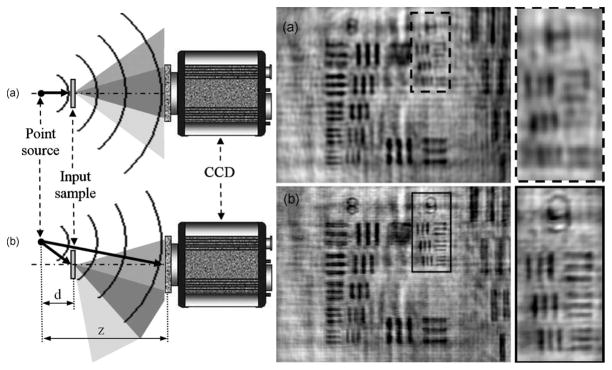
(Left) Schematic diagram of the Super-resolution DIHM setup with on-axis (a) and off-axis (b) illumination. (Right) Experimental results for laser (λ=405 nm) point source illumination and 1951 USAF resolution test target. (Top) reconstructed image using conventional DIHM and (Bottom) reconstructed image using super-resolution DIHM. Reprinted from [40] with permission from SPIE.
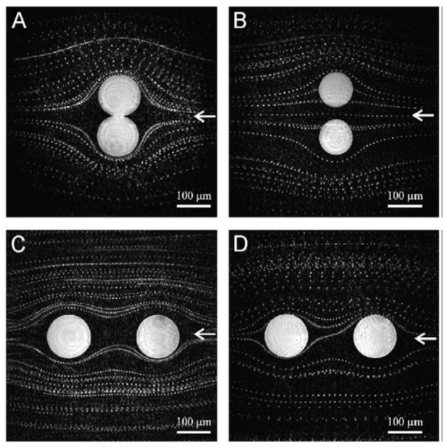
For the in-line hologram recording geometry outlined in Figure 2, the spatial and temporal coherence of the illumination has to be high, so that the object wave and the reference wave can interfere at the detector-array. Due to the relatively large distance between the object and the sensor planes, the scattered object wave fills a substantial area on the image sensor, especially when the system tries to capture the light at high angles for increased resolution. Consequently, the whole sensor surface needs to be coherently illuminated, requiring a large spatial coherence diameter as well as the use of a narrowband light source such as a laser for getting sufficient temporal coherence. The aperture used for spherical wavefront generation (Fig. 2) typically has a submicron diameter, thus it automatically provides the required spatial coherence. On the other hand, an increase in spatial and temporal coherence can cause unwanted interference terms due the reflective surfaces in the system and is a source of multiple reflection interference and speckle noise. Light emitting diodes (LEDs) can also be used for illumination, as demonstrated by Repetto [43], but since their coherence length is in the micrometer range one has to carefully consider the spectral characteristics of the used LED for an optical set-up as shown in Fig. 2, where the sample is quite away from the detection plane. Nevertheless, several systems using lasers or partially temporally coherent light sources have been used for imaging biological samples, such as diatoms [44], dinoflagellates [45] and other aquatic life-forms [46] as well as for visualizing fluid flow patterns [47] (see Fig. 5), and investigation of the behavior of microbial life forms in fresh water [48].
Fig. 5.
Fluid flow visualization using bovine red blood cells with DIHM. The liquid is coming from the direction of the arrows, and is flowing around two fixed spheres in different geometries. Reconstructions are made from difference holograms composed of 100 holograms taken at 10 frames per second, using a green laser that illuminates a 1 μm pinhole. The pinhole to sample distance is 1 mm and the NA is 0.25. Reprinted from [47] with permission from Elsevier copyright (2008).
One practical limitation of these systems is that pinholes of such a small size tend to get blocked by dust or other particles easily, and the proper adjustment of such a pinhole to a focused laser beam requires high precision and could also require relatively expensive optical and mechanical elements.
As a modified scheme compared to Figure 2, optical ptychography (which relies on coherent diffraction) has also been used for lensless microscopy purposes [49], [50]. In this approach, the sample is mechanically stepped through a localized coherent wavefront generating a series of diffraction patterns on the detector array. From these coherent diffraction measurements, the phase and amplitude of the object can be reconstructed iteratively. This method requires precise control of the sample position and acquires more number of images than the in-line holographic method depicted in Fig. 2. However, using super-resolution methods it can also perform high-resolution microscopy with a long working distance, without being limited by twin image problems.
In the next sub-section we will discuss an alternative inline holographic imaging modality which is based on partially-coherent planar illumination. Some of the important advantages of this approach would be to achieve a significantly larger imaging FOV while also using very large illumination apertures (bringing alignment simplicity) as well as reducing speckle and multiple reflection related noise artifacts observed in reconstructed images.
B. Digital in-line holographic microscopy with partially-coherent planar wavefront illumination
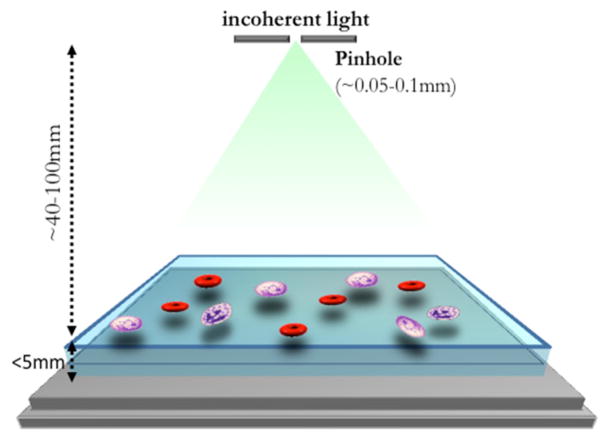
For imaging applications that demand a large FOV and high throughput, digital in-line holography can efficiently use the full active area of a given image sensor chip by changing its optical setup as shown in Fig. 6 [41], [42], [51–54].
Fig. 6.
Illustration of the on-chip lensfree holography platform. A partially coherent light source (e.g., an LED) is used to illuminate the sample which is placed less than 5 mm from the image sensor. The pinhole is placed at ~ 4–10 cm away from the sensor surface to record the digital in-line holograms of specimens with unit fringe magnification. The FOV of the microscope is equal to the active area of the image sensor chip, e.g., 24 mm2. Reprinted from [55] with permission from IEEE.
An important difference that we would like to initially point out in Figure 6 compared to the holographic imaging architectures discussed in the previous section is that the sample to sensor distance (z2) is much smaller than the distance between the sample and the light-source/pinhole(z1).
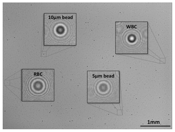
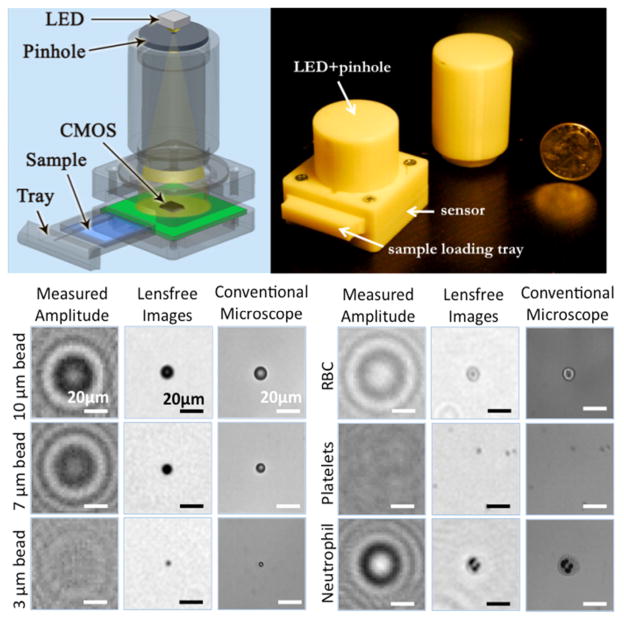
This leads to a new type of digital holographic system, with several unique features. First, the fringe magnification (M) of this system is approximately 1, which leads to an imaging FOV that equals to the active area of the sensor chip e.g., ~24–30 mm2, as shown in Fig. 7. Second, since the illumination source is placed far from the sensor plane, the reference wave can be considered as a plane wave, and therefore the digital reconstruction does not have the same sampling and aliasing related issues that spherical wavefronts have. Third, in this new geometry the main limiting factor for spatial resolution is actually the physical pixel size and not the width of the used image sensor. Fourth, both the spatial and temporal coherence of the used illumination can now be significantly lower, since the path length difference between the scattered and the reference wave and the spatial size of the recorded hologram of a single object (e.g., a cell) is substantially smaller. It can be shown [51] that the use of spatially incoherent illumination through a large aperture is approximately equivalent (for each cell’s holographic signature) to spatially coherent illumination of each cell individually, as long as the cell’s digitally sampled hologram is smaller than the spatial coherence diameter at the detector plane. For a typical setup as shown in Fig. 6, the spatial coherence diameter is ~200–500μm, which is quite appropriate for most cells of interest. This means that the light source can now be a simple LED that is butt-coupled to a large pinhole or a large-core multi-mode fiber, and thus no sensitive alignment or light-coupling optics is needed. Consequently, the entire lensfree on-chip holography platform lends itself to a compact, cost-effective and mechanically robust architecture, which can be especially useful to build microscopes for field-use in low-resource settings, or to integrate with compact on-chip microfluidic systems. Finally, the reduced coherence of this platform also significantly reduces speckle, multiple reflection noise as well as the cross-interference among scattered object waves, which all represent noise terms in a reconstructed holographic image. Biomedical use of this platform has already been demonstrated for blood analysis [51], [52] (See Fig 8.), for imaging antibody microarrays [56], for semen analysis [57] and for the detection of waterborne parasites [58].
Fig. 7.
A full FOV lensfree in-line hologram of a heterogeneous sample containing white blood cells (WBCs), 10 μm micro-particles, red blood cells (RBCs) and 5 μm micro-particles. It was recorded using a 5MP sensor with 2.2 μm pixel size. The total imaging area of the sensor and the FOV of the system is ~24 mm2, i.e., more than 10 fold larger than that of a standard 10× objective lens. The insets show individual lensfree holograms that can simultaneously be reconstructed to obtain microscopic images. Reprinted from [55] with permission from IEEE.
Fig. 8.
Schematic view and a photograph of the lensfree telemedicine microscope. Measured holograms and reconstructed lensfree images of various micro-objects such as micro-beads, human RBCs, WBCs and platelets are shown, and are compared against 40× objective-lens (NA: 0.65) microscope images of the same objects. [51] - Reproduced by permission of The Royal Society of Chemistry.
Although the large FOV, reduced interference noise and alignment simplicity are important features of this optical setup, it also introduces new challenges. Due to the short sample to detector distance, the diameter of the twin image at the object plane now gets smaller, and therefore the elimination of the twin image becomes more important. In addition to this, due to unit fringe magnification of this hologram recording geometry, the pixel size at the detector array now plays an important role in spatial resolution, since it may cause under-sampling of high-frequency fringes of a lensfree hologram. For applications that require submicron resolution, this spatial resolution limit imposed by the pixel size can be circumvented through use of pixel super-resolution algorithms, as first demonstrated for lensfree on-chip imaging by Bishara et al.[41] (see Fig. 9).
Fig. 9.
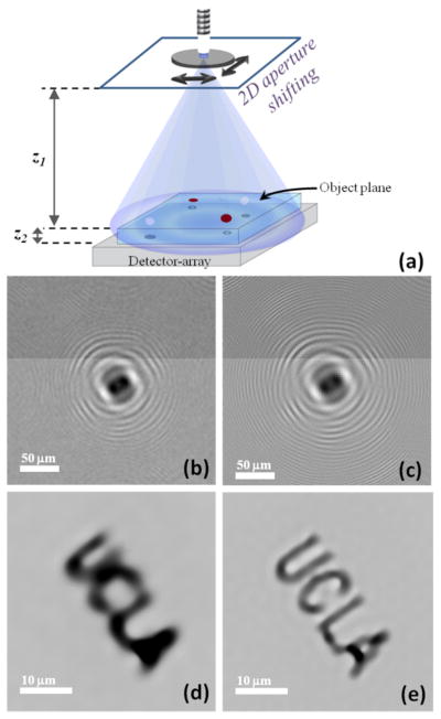
Pixel super-resolution system for lensless in-line holographic microscopy. (a) Typical schematic diagram of the lensfree microscope with source shifting. (b) An example of a single low resolution hologram; (c) super resolved hologram of the same object. (d) Reconstruction of (b). (e) Reconstruction of (c). Adapted from [41], [42] - Reproduced by permission of OSA and The Royal Society of Chemistry, respectively.
Although this super-resolution method also involves capturing several lensfree holograms of the same object, the idea behind it is rather different. The resolution loss in Fig. 5 is not caused by the loss of light diffracted at high angles, since even light rays corresponding to an NA of ~1 can now reach the detector surface. The problem is caused by the under-sampling of the lensfree holograms by the detector pixels. Information of these high spatial frequency fringes can be recorded indirectly as slight variations in the pixel values corresponding to spatial aliasing (see Fig. 9). By recording several lower resolution lensfree holograms that are sub-pixel shifted with respect to each other over the detector active area we obtain slightly shifted versions of a single high-resolution hologram that was under-sampled by the sensor array. The required sub-pixel shifts of the holograms on the sensor plane can be created by e.g., shifting the light source [41], [42]. The spatial aliasing of the lower resolution holograms can then be digitally resolved using all these recorded shifted holograms. To synthesize this pixel super-resolved hologram, the exact shifts of these low resolution holograms with respect to each other have to be known. To accurately determine these shifts from the captured lensfree images, gradient-based iterative shift estimation methods can be utilized [41]. Once the hologram shifts are digitally estimated, the super-resolved hologram with a smaller effective pixel size can be iteratively calculated using a cost-function and sub-sequent optimization. An extension of this pixel super-resolution approach has recently enabled a high numerical aperture of ~0.9 achieving ~300 nm half-pitch resolution across a large FOV of >20 mm2 [59].
One practical realization of this method involves the use of a matrix of fiber-coupled LEDs (Fig. 10). The sub-pixel shift of each lensfree hologram is achieved by changing the position of the illumination fiber, which here is created by individually turning on one of the LEDs at a time, thus no moving parts are required. This method has been successfully used for imaging of malaria infected red blood cells over a large FOV of e.g., 24 mm2 [42] (see Fig. 10).
Fig. 10.
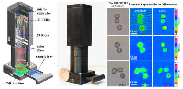
(Left) CAD drawing and (Middle) photograph of the portable lensfree super-resolution microscope (weight ~95 grams). The light source consists of 23 LEDs coupled to 23 multi-mode fiber-optic cables without the use of any lenses or other opto-mechanical components. Each LED is sequentially turned on to create subpixel shifted lensfree holograms of the objects on a CMOS sensor-array with 2.2 μm pixel-pitch. These recorded lensfree holograms can be rapidly processed using a pixel-super-resolution algorithm to create lensfree images of the objects with <1 μm resolution over an FOV of >24 mm2. (Right) Reconstructed super-resolved images of standard thin smears of human RBCs that were infected with malaria parasites (Plasmodium falciparum). The parasites can be clearly seen in both amplitude and phase images. Bright-field microscope images (0.65-NA, 40×) of the same samples are also shown. [42] - Reproduced by permission of The Royal Society of Chemistry.
As an alternative approach, pixel super-resolution in a partially-coherent in-line holographic system can also be achieved by moving the sample instead of the light source, e.g., by imaging flowing cells in a microfluidic channel as demonstrated by Bishara et al.[60].
Although the above discussed pixel super-resolution methods break the resolution barrier imposed by the pixel size of the detector, they are fundamentally limited by the detection signal-to-noise ratio (SNR) of the captured lensfree holograms. As a potential solution to this and hence to increase the detection SNR, the use of thin wetting films [61] during the sample preparation process is shown to increase the intensity diffracted to high spatial frequencies, thus enabling the visualization of weakly scattering objects, such as E. coli particles [62].
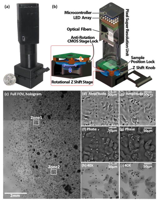
The same partially-coherent imaging platform of Fig. 6 is also capable of color imaging as demonstrated by Isikman et al. [63]. Recently, a modified version of this setup was also used for screening of dense pathological slides (Papanicolaou smears) over a large FOV of 30 mm2. Here, the phase recovery was done iteratively by using several lensfree transmission holograms acquired at different sample to sensor distances [21], [54] (see e.g., Fig. 11). These results discussed so far illustrate that the in-line digital holographic microscopy techniques provide comparable image quality to conventional lens-based microscopes for various biomedical applications.
Fig. 11.
Multi-height lensfree on-chip imaging system (a) photo, (b) system schematic, and (c–i) results for a dense Papanicolaou smear sample are summarized. (c) A full FOV (~30 mm2) holographic image taken with the field-portable lensfree microscope. (d and e) Reconstructed amplitude images of zones 1 and 2, cropped from (c). (f and g) Reconstructed phase images of zones 1 and 2, cropped from (c). Images (d–e) are calculated using holograms from 5 different heights and a total of 10 iterations. (h and i) Microscope images (40× objective, 0.65 NA) of the same regions for comparison purposes. [54] - Reproduced by permission of The Royal Society of Chemistry.
In addition to achieving sub-micron resolution over a large FOV (e.g., 20–30 mm2), with these techniques the sample of interest does not necessary have to be planar; i.e., volumetric imaging is also possible. Since the reconstruction (i.e., focusing) is done numerically, the system is capable of performing a numerical equivalent of a Z-scan from a single lensfree hologram.
An important drawback of the above discussed holographic systems is the need for transparent samples since these microscopes work in transmission mode. Extension of similar ideas to reflection geometry has also been demonstrated [25], however, these approaches need further improvements to reach the throughput and the space-bandwidth of their transmission counterparts.
Another limitation of these digital holographic microscopes can be considered as their need for computation to reconstruct images. On the other hand, the speed and capabilities of our digital processors have reached a decent level which makes real-time numerical reconstruction possible on e.g., graphics processing units (GPUs) which have already appeared even on our smart-phones. Therefore, our global access to such advanced computational resources within inexpensive and compact embodiments makes it quite timely to practice such lensfree digital holographic microscopes even in resource limited settings. Thus, cost effectiveness of these platforms is also a major benefit since the imaging system can be assembled from inexpensive off-the-shelf components, without the need for special manufacturing requirements.
III. Non-holographic Shadow Imaging On a Chip
In this section, we will focus on non-holographic shadow imaging systems, where the diffraction patterns of incoherently (or partially-coherently) illuminated objects are digitally sampled by a detector array. The key distinction between these shadow imaging approaches and the lensfree holographic techniques discussed in the previous section is that in lensfree holography, digital refocusing of object waves is used to image a given object/sample plane regardless of optical diffraction, whereas in shadow imaging approaches the diffraction between the object and detector planes is either ignored or is left unprocessed.
As an example, in 2005 Lange et al. demonstrated [64] that a compact microfluidic chamber combined with a CMOS image sensor can be used to study the behavior of Caenorhabditis elegans in Space.
As shown in Fig. 12, one of the main differences from the previously discussed lensfree architectures is the use of spatially and temporally incoherent illumination. This shadow imaging method has some similarity with partially coherent imaging methods of the previous section, since the FOV is also equal to the whole sensor active area. However, the non-coherent and uncontrolled nature of the illumination prevents the use of wave propagation algorithms to digitally undo the effects of diffraction. Since diffraction is practically unavoidable, these captured lensfree shadow images are not identical to the object itself, but can represent a spatial characteristic signature of it, e.g., similar to a ‘fingerprint’. The spatial resemblance of the object to its shadow strongly depends on (1) 3D nature of the object since for each sample only a 2D shadow is measured without the ability to digitally refocus or reconstruct; (2) the sample to detector-array distance; and (3) the pixel size (causing pixelation).
Fig. 12.
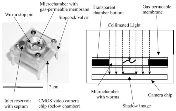
Photograph and schematic diagram of the lensless nematode shadow imager. Specimens are swimming within a 500 μm high chamber and are illuminated with an LED. The shadows of the objects are recorded using a CMOS image sensor attached to the bottom of the chamber. Reprinted from [64] with permission from Elsevier copyright (2005).
Nevertheless, this incoherent shadow imaging geometry was successfully used for different wide-field on-chip imaging applications [65]. Since the features of the diffracted pattern are affected by e.g., the shape of the object, they can be used for counting of cells [66]. The main advantage of this system is its simplicity for screening a large FOV and reduced computational power need. One obvious drawback of this approach, however, is that the output shadow images, while containing useful fingerprint information, cannot reveal microscopic spatial features of the specimen. This makes it harder to operate especially if there is spatial overlapping among shadows of different objects, making interpretation of the acquired shadow images challenging for dense samples.
To mitigate this challenge and obtain high resolution microscopic images using incoherent shadow imaging, one has to significantly decrease the sample to sensor distance to ‘minimize’ the effect of optical diffraction. This method is also referred to as contact imaging. The removal of color filters and the microlens array that are typically installed on image sensor chips can provide a vertical distance adequate for microscopy purposes. However, for making use of such a processed sensor chip, the cells have to be seeded directly onto the sensor surface. In this contact imaging geometry, to overcome the resolution limit imposed by the pixel size of the CMOS sensor, the source-shifting based lensfree super-resolution approach presented in Refs. [41] and [42] has been applied to claim an improved resolution compared to the physical pixel size of the sensor-array [67].
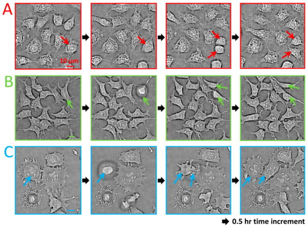
Since these imaging systems are compact they can also be placed into an incubator as demonstrated by the “ePetri dish” (see Fig. 13) [67]. The ePetri platform can provide time lapse imaging of the evolution of a cell culture, and can detect and track each individual cell’s movements in space and time to generate corresponding lineage trees (i.e., mother-daughter relationship).
Fig 13.
Contact imaging results based on “ePetri dish”. This system is able to track cell division events (shown by the arrows) for various cell types. Images shown here are obtained sequentially at three different locations (A,B,C) of the same image sensor with ~30 minute time increments. When a cell division occurs, the cell detaches from the sensor surface and the sample to sensor distance considerably increases, creating spatial aberrations. Reprinted from [67] with permission from PNAS.
Due to its ‘contact’ geometry, the ePetri platform has some advantages and disadvantages compared to the previously discussed approaches. Since the object is only ~0.9 μm away from the active area of the sensor chip, a decent image might be reconstructed for 2D objects without the need for computationally addressing optical diffraction. This makes the ePetri platform image dense and flat objects relatively easier compared to e.g., multi-height holographic lensfree imaging approach discussed in Fig. 11.
However, being a contact imaging platform, ePetri cannot handle 3D objects unlike holographic approaches and also suffers from a quick loss of resolution as the sample to sensor distance increases by even a few hundred nanometers (see Figs. 13 and 14). Moreover, the temperature increase of the sensor during operation can affect the sample that is in contact, which might have some practical limitations for biomedical samples.
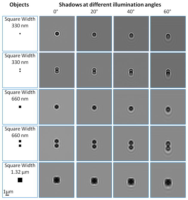
Fig 14.
Lensfree shadow images of various objects are simulated under different illumination angles. The objects are assumed to be two-dimensional only (i.e., flat as desired by contact imaging), positioned on a 1.45 refractive index layer at 0.9 μm away from the active region of a detector-array. Experimental conditions of the ePetri system in terms of source spectrum, source-sample-detector distances and illumination angles are used [67]. Pixel size is 10 nm, mimicking a theoretically perfect pixel super-resolution performance. Even in this best case scenario severe spatial distortions for sub-micron object features are observed for a contact imaging platform.
In addition to these, the short sample to sensor distance (e.g., ~0.9 μm - which is needed to for contact imaging to work as a microscope) requires the use of large illumination angles (e.g., up to ±60° as used in [67]) to perform pixel super-resolution; otherwise the required pixel shifts cannot be achieved, significantly limiting the resolution of the technique. However, such large illumination angles might bring fundamental limitations and artifacts, as illustrated in Fig. 14, and therefore should be handled with care. Specifically, at high illumination angles required by ePetri platform, the object-sensor distance increases, which makes optical diffraction more pronounced for sub-micron features of an object (see Fig. 14). This suggests that for such high angles, the shadows of the objects with a contact imager start to “significantly” differ from the real object images. Furthermore, even for flat samples, the shadows of micron-scale objects will also be physically stretched (i.e., asymmetrically widened) at the detector-plane with increasing illumination angles. Therefore, under large illumination angles the recorded micro-shadows will ‘not’ be shifted versions of the ‘same’ object-function (see e.g., Fig. 14), which would introduce artifacts during pixel-super-resolution steps.
In contrast, the digital holographic super-resolution techniques discussed in the previous section use significantly smaller illumination angles (<1–2°) due to the larger sample to detector distance. As a result of this, object cross-section changes and asymmetric shadow stretching at the detector-array can be truly ignored [41],[42]. In fact, if these different cross-sections were preserved under wide-angle illumination, and if appropriate processing was used to account for micro-shadow stretching at the detector-array, lensless tomographic microscopy can be demonstrated as will be discussed in Section IV.
In all these shadow imaging platforms discussed above, including contact imagers, the partial coherence of the illumination [68], [69] also has to be carefully considered since it will create artificial oscillations in object shadows due to partial interference of light. As an example, to obtain the temporal and spatial coherence conditions of the system reported in Figs. 13–14, we measured the spectral output of the illumination source (for temporal coherence) and also calculated the spatial coherence diameter of the light spots used for illuminating the sample [67]. Based on these calculations, the light impinging on the detector-array can be found to be partially-coherent (both spatially and temporally) which directly implies that the shadows of two closely-spaced micro-objects (e.g., ≤1 μm apart) would interfere with each other and with the background-light at the detector plane, making the interpretation of the observed micro-features in a shadow image (after e.g., pixel-super-resolution) rather difficult (see Fig. 14 for some examples of this phenomenon).
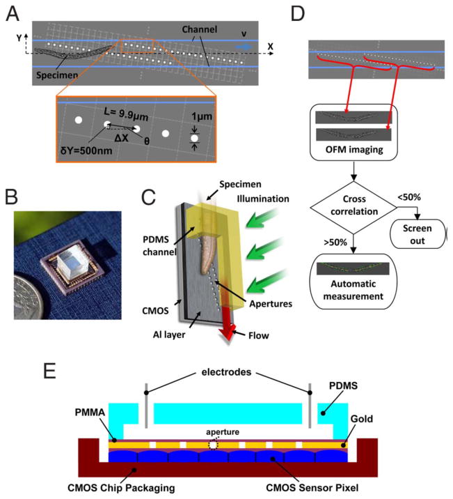
Some of these issues discussed above for contact imaging approaches can be better handled through introduction of even smaller pixel size sensor-arrays, with a pitch of e.g., ≤ 1μm. Another elegant approach for addressing the resolution issues of a contact imaging geometry was published by Heng et al. to create an optofluidic microscope (i.e., OFM) [70]. Similar to the previously discussed super-resolution methods, the idea requires several images to be captured from the same object, and in this case it is achieved by moving a sample in a microfluidic channel. To overcome the distance and pixel size limitations, a linear array of circular apertures, each with submicron diameter, was fabricated. The optical transmission through each aperture should map uniquely onto a single sensor pixel and therefore the spacing between the pinholes should be equal to the pitch size of the image sensor. The angle between the pinhole array and the flow direction inside the microfluidic channel has to be chosen such that each neighboring aperture should overlap by at least half the aperture size if projected to the plane perpendicular the flow direction (See Fig. 15).
Fig. 15.
Optofluidic microscope (OFM) prototype. (A) Schematic top view of the OFM. The OFM apertures (white circles) are placed on the Al (gray) coated 2D CMOS image sensor (light gray dashed grid) and extend across the whole microfluidic channel. (B) The actual device next to a U.S. quarter. (C) Vertical operation mode. (D) Flow chart of the OFM operation. Two OFM images of the same C. elegans are acquired by the two OFM arrays as shown by the red arrows. If the correlation between the two images is <50%, these images are rejected. Otherwise, the area and the length of the worms are automatically determined. (E) Cross-sectional view of an electro-kinetically driven OFM device. [71] Copyright (2008) National Academy of Sciences, USA.
The flow of the samples inside the chamber can be created by gravity, pressure, electro-kinetical methods [71], or with an optical tweezer system [72]. This architecture performs a line scan of the target specimen with an increased resolution compared to the pixel size of the used sensor-array, since the resolution now depends on the diameter of the used apertures (assuming that the gap between the object and the aperture plane is negligibly small – a topic which will be discussed in the next paragraphs) [73]. An important assumption in this approach is that the object’s orientation and shape remains unchanged until it fully passes over the apertures. Although the use of reduced number of pixels makes it possible to reach a high frame-rate (e.g., 1000 frame/sec with a flow rate of 500μm/sec), even a small shift of objects occurring during image capture can cause distortions. More importantly, the flow speed of the sample has to be accurately set to be able to reconstruct two dimensional images. Although this parameter is measured by the system itself, through the use of two parallel aperture lines, this phenomenon caused rejection of ~50% of the samples for initial designs of this platform. Recent results based on the same technology improved this object rejection rate by using e.g., electro-kinetical methods.
Another important factor that needs to be considered in an OFM design is that decreasing the aperture size also decreases the depth of field of this system, and therefore to achieve the best possible resolution, the object has to be as close to the aperture grid as possible; and it has to be flattened out such that a uniform lateral resolution can be claimed. Similar to the ePetri platform discussed earlier, even 1 μm vertical gap between the aperture plane and the objects can cause severe resolution penalties for practical objects.
This OFM system has been successfully used to measure biological samples, such as blood cells, and various pollen spores (see Fig. 16.). A new version of this architecture, capable of color image acquisition has been recently reported by Pang et al.[74].
Fig. 16.
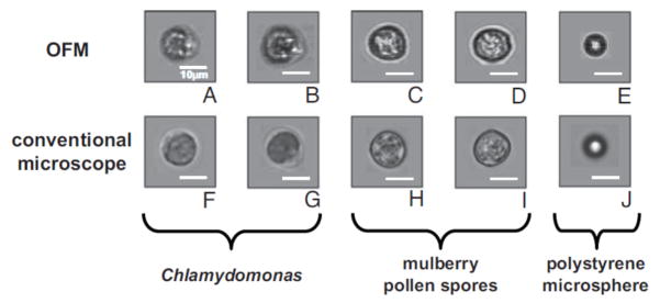
Cell and microsphere images captured by the electrokinetically driven OFM (A–E), and the corresponding microscope comparisons taken by a light transmission microscope with a 20× objective (F–J). Objects are Chlamydomonas (A,B and F,G), mulberry pollen spores (C,D, and H, I), and 10-μm polystyrene microspheres (E and J). Scale bars are 10 μm long. [71] Copyright (2008) National Academy of Sciences, USA.
On-chip imaging can be also done with the use of structured surfaces as optical components. As an example, the use of diffractive lenses, such as Fresnel zone plates, to enhance the imaging capabilities and the resolution of a wide field-of-view lens based system for imaging cells in microfluidic chambers, has been demonstrated by Schonbrun et al.[75]. Diffractive lenses can be patterned using a single lithographic step and are compatible with standard microfluidics fabrication techniques because they can be molded into polydimethylsiloxane (PDMS). These lenses change the direction of incident light by using a thin and planar grating pattern, thus they are suitable components for compact imaging systems. They can also serve as relay lenses for some on-chip imaging systems, creating a distance between the sensor and the sample and solve the problem of heat transfer between the sample and the sensor [76]. Using structured metal-dielectric surfaces, one can also create custom optical transfer functions [77], such as spatial filters for darkfield imaging needs [78].
IV. On-chip Tomography
Microscopy is not the only imaging modality that can be accomplished in a compact, on-chip setup. Obtaining high resolution three-dimensional volumetric information of specimens has recently came to focus, and several lens based digital holographic approaches have been published [79–82]. Since we focus on methods that can be used for compact, cost effective, on-chip systems, we will only review the recent lensless tomographic imaging systems; further details of tomographic diffractive microscopy techniques in general can be found in other review articles, see e.g., [83]. Even though digital holographic microscopy can in principle enable 3D imaging by digitally reconstructing the holograms at different depths, its low axial-resolution does not permit truly tomographic imaging. Axial-resolution also depends on the size of the object, as DOF is comparable to the far-field distance of a particle which is proportional to a2/λ, where a is the particle diameter, and λ is the wavelength of illumination [84].
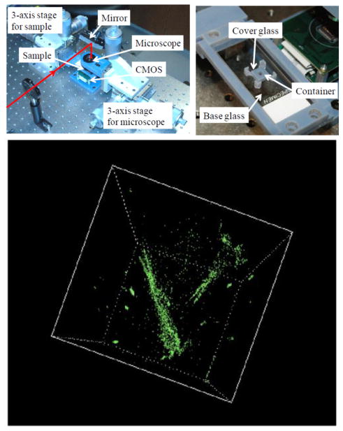
Therefore, reconstructing a hologram at different planes along the optic axis, which is essentially equivalent to numerically propagating the optical field to different planes through the object, does not necessary provide 3D structural details with sufficiently high resolution especially for relatively large objects (e.g., >10–20μm). Using compressive holography techniques [86], [87] to reconstruct in-line holograms that were captured with the geometry reviewed in Section II, one can circumvent this problem and create tomographic reconstruction [85] (see Fig 17).
Fig. 17.
Photographs of the holographic microscopy system (top left) and the fluidic chamber in which water cyclopses are swimming (top right). A 3D image of the compressive holographic reconstruction of water cyclopses (bottom). The spatial resolution of this system is approximately 2.2 μm (lateral) together with an axial resolution of ~59 μm. Reprinted from [85] with permission from OSA.
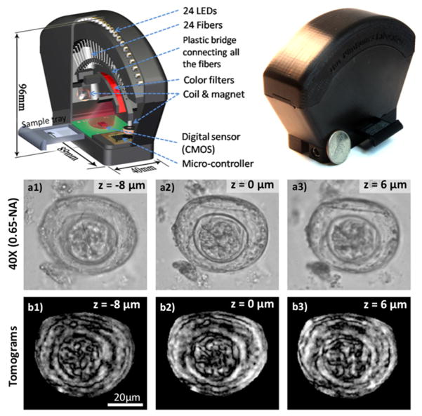
Another approach to increase the axial resolution of the digital in-line holographic microscope discussed in Section II. B. has been demonstrated by Isikman et al. [53] (see Fig. 18). The idea behind this approach is to synthesize several lensfree super-resolved holograms of the samples by varying the direction of the illumination over a large angular range of e.g., ±60° in order to obtain 2D projection images of objects from multiple viewing directions. 3D tomographic images of the objects can then be numerically computed with significantly improved axial resolution from these 2D projection images by using a filtered back-projection algorithm that is commonly employed in X-Ray and electron tomography schemes [88]. This technique achieves a 3D spatial resolution of <1μm × <1μm × <3μm (in x, y and z, respectively) over a large imaging volume of e.g., 15 mm3 and has been successfully used for imaging of C. elegans worms [89] (see Fig. 18b). Furthermore, a field portable version, weighing only ~110 grams, of the same architecture was also constructed to image Hymenolepis nana eggs [90] (See Fig. 19).
Fig. 18.
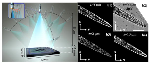
Schematic view of the lens-free tomography setup (left), and experimental results of the system (right). The sample is placed <4 mm distance from the active area of the image sensor. A partially coherent light source is coupled to a multimode fiber with a diameter of approximately 0.1 mm. The fiber-end is rotated to record lens-free holograms of the micro-objects from multiple viewing angles. (b1) A single plane of the tomogram of a C. elegans nematode, and (b2) the microscope image of the same plane. (b3–b4) Image planes at different depths of the same tomogram. Reprinted from [53] with permission from PNAS.
Fig. 19.
Schematic view (top left) and a photograph (top right) of the field-portable lensfree tomographic microscope, which weighs ~110 grams. The light source consists of 24 LEDs coupled to 24 multi-mode fiber-optic cables without the use of any lenses and are mounted along an arc to provide illumination with an angular range of ±50°. Each LED is sequentially turned on to capture lensfree holograms at each angle. The sub-pixel shifts of these holograms are achieved by electro-magnetically shifting the fiber-ends. (a1–a3) Microscope images (40× objective, 0.65 NA) of different focal planes of a H. Nana egg (z-scan) are shown for visual comparison. (b1–b3) Computed tomograms for different depths of the same H. Nana egg. [90] - Reproduced by permission of The Royal Society of Chemistry.
This system is limited by the acceptance angle of the used CMOS sensor, and obtaining tomographic reconstructions is computationally more demanding than regular digital holography. Nevertheless, the handheld implementation proves that cost effective and compact on-chip imaging systems can perform tasks that would normally require rather expensive and bulky optical imaging instruments/designs.
Obtaining a tomographic image from biological samples on a chip has also been demonstrated by measuring the electrical impedance of cells [91]. The main advantage of this approach is its high temporal resolution, however the image quality and resolution are currently behind the presented optical approaches.
V. Lensfree Fluorescent Imaging On a Chip
Fluorescent microscopy remains as one of the most widely used methodologies in biotechnology, since it offers exquisite sensitivity and compatibility with standard biochemical reactions. The on-chip integration of excitation light sources, such as VCSELs [92–95] or LEDs [96] as well as photo-detectors was already accomplished almost a decade ago. These existing systems demonstrated their promising potential in several biomedical applications, such as DNA analysis [97], or the determination of urinary human serum albumin [98]. Eliminating the excitation light while detecting most of the emitted light is as important in these compact systems as in regular fluorescent microscopes, and several novel filter structures were designed for this purpose [99–101]. On-chip spectrometers analyzing the fluorescence of moving objects had also been constructed by combining a linear variable band-pass filter with a CMOS camera to convert the spectral information of the incident light into a spatial signal [102].
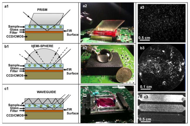
Integrated on-chip architectures using image sensor-arrays for measurement of fluorescent microarrays showed a significant improvement over regular microscope based systems in terms of e.g., signal to noise ratio and sensitivity [103]. The optical characteristics of these integrated lensless bio-photonic imagers differ from regular fluorescent microscopes, since there are no lenses to focus the emitted light. Fluorescent light is ‘usually’ not suitable for holographic recording, thus wave propagation algorithms cannot provide focusing. One notable exception to this was published by Rosen et al.[104], where the authors used a spatial light modulator to create self-interference with the emitted fluorescent light in their lens based fluorescent holographic microscopy system. However, in a general lensless fluorescent imaging system, “focusing” is created by deconvolving the captured image with the point spread function of free space propagation [105], [106] instead of using wave propagation algorithms. Examples for various optical setups are shown in Fig. 20. The fluorescent excitation light enters at a high angle into the sample chip and, after interacting with the sample volume, is reflected through a total internal reflection (TIR) process occurring at the bottom facet of the sample holder. The light emitted by the excited cells or particles has angular isotropy, so it does not get totally reflected, and therefore can be directly detected and sampled without the use of any lenses over the entire FOV of the sensor chip. Quite importantly, the numerical aperture of such on-chip systems is close to 1, since the large-area detector is placed very close to the fluorescent micro-objects, thus this architecture excels at photon collection efficiency. Since no lenses are involved in imaging, the fluorescent emission of cells or particles will diverge rapidly, potentially overlapping with each other at the sensor plane. However, the 3D distribution of the fluorescent objects can be reconstructed from these overlapping out-of-focus lensfree image through e.g., deconvolution [106] or compressive decoding techniques [108], [109]. The resolution of such systems depends on the sample to sensor distance, and therefore it is advantageous to make these systems as compact as possible. However, the heat transfer between the sensor and the sample and other practical limitations such as contamination of the active region of the sensor-array also have to be considered. The use of compact optical elements, such as nanostructured surfaces [110] or tapered fiber optic faceplates [111] has been recently demonstrated, increasing the resolution of these wide field-of-view incoherent systems down to <4μm. These fluorescent imaging modalities can be combined with on-chip bright field methods to create multi-modal, and yet cost-effective and field-portable microscopy platforms that can perform both bright-field and fluorescence on-chip imaging.
Fig. 20.
On-chip microscopy platform for lens-free fluorescent imaging over a large FOV of e.g., 2.5 cm × 3.5 cm. Different illumination and excitation configurations are shown (a, b, c). Schematic diagrams (a1, b1, c1), corresponding experimental set-ups (a2, b2, c2) and typical wide-field fluorescence images (a3, b3, c3) are presented. Reprinted from [107].
Optofluidic microscopy systems are also capable of fluorescent detection through use of e.g., planar lenses. For instance, a compact Fresnel zone plate array based fluorescent optofluidic microscope has been recently demonstrated by Pang. et al.[112].
VI. Future Prospects and Conclusions
The role of lab-on-a-chip diagnostics in biomedicine gradually increased in the past decade due to the need for more cost effective, complex and yet portable systems. The possibility to acquire multi-parametric information from a single sample can lead to new types of point-of-care diagnostic tools, and it might especially prove useful for personalized medicine, screening and monitoring of patients, as well as customized therapy. Recently, several point-of-care diagnostic devices have also appeared on the market, such as Magnotech from Philips, DXpress Reader from Life Sign LLC, Qualigen Fast Pack IP from Qualigen, where these systems aim detection of e.g., DNA, protein or small molecules. To make such systems even more powerful, extensive research has been conducted toward integration of active components on a modular chip, such as pumps, valves, and temperature controllers [113]; and also compact digital microfluidic systems are devised to perform cell culturing and analysis on a single chip [114]. In this manuscript, we reviewed several modalities that can function as on-chip biomedical imagers. Using these on-chip imaging platforms, integrated on-chip microfluidic systems can further include microscopic imaging as one of their key components and potentially expand the palette of multi-parametric diagnostics. Quite importantly, the rapid development of sensor-array technologies, in particular CMOS and CCD imagers, will be further improving the performance of on-chip microscopy systems. As an example, the field-of-view of partially coherent lensless inline holographic microscopy increased from e.g., 24 mm2 [42] to 30 mm2 [54] within a single year, while keeping the resolution still at deeply sub-micron level. In the next decade these lensless on-chip imaging systems will continue to improve in terms of both field-of-view and resolution (see e.g., [59]), and with the rapid increase of computational power (especially GPUs), real time systems will also be introduced soon. Finally, we should emphasize that the rapid pace of such developments makes it rather difficult to create a comparison table in terms of performance with exact numbers since within less than 1–2 years such a table will quickly be out of date and therefore could be misleading.
Acknowledgments
A. Ozcan gratefully acknowledges the support of the Presidential Early Career Award for Scientists and Engineers, Army Research Office Young Investigator Award, National Science Foundation CAREER Award, Office of Naval Research Young Investigator Award and National Institutes of Health Director’s New Innovator Award DP2OD006427 from the Office of the Director, National Institutes of Health.
Biographies
 Zoltán Göröcs received his M.S. degree in physics and Ph.D. in physics from the Budapest University of Technology and Economics, Budapest, Hungary, in 2003 and 2011 respectively.
In 2007 he spent one year as a Research Intern at Corporate Research & Development Center, Toshiba Corp. in Kawasaki, Japan. In 2009 he joined the Computer and Automation Research Institute of the Hungarian Academy of Sciences as a Research Fellow. He is currently a Postdoctoral Fellow in the Department of Electrical Engineering, University of California, Los Angeles (UCLA), investigating digital holographic imaging devices. His research interests include acousto-optics, electro-optics, optical signal processing, holography, digital holography and image processing.
 Aydogan Ozcan (SM’10) Dr. Aydogan Ozcan received his Ph.D. degree at Stanford University Electrical Engineering Department. After a short postdoctoral fellowship at Stanford University, he is appointed as a research faculty at Harvard Medical School, Wellman Center for Photomedicine in 2006. Dr. Ozcan joined UCLA in the summer of 2007, where he is currently an Associate Professor leading the Bio- and Nano-Photonics Laboratory at the Electrical Engineering and Bioengineering Departments.
He holds 21 issued patents and more than 15 pending patent applications for his inventions in nanoscopy, wide-field imaging, lensless imaging, nonlinear optics, fiber optics, and optical coherence tomography. He gave more than 120 invited talks and is also the author of one book, the co-author of more than 250 peer reviewed research articles in major scientific journals and conferences. In addition, He is the founder and a member of the Board of Directors of Holomic LLC. He received several major awards including the 2011 Presidential Early Career Award for Scientists and Engineers (PECASE), which is the highest honor bestowed by the United States government on science and engineering professionals in the early stages of their independent research careers. He received this prestigious award for developing innovative optical technologies and signal processing approaches that have the potential to make a significant impact in biological science and medicine; addressing public health needs in less developed countries; and service to the optical science community including mentoring and support for underserved minority undergraduate and graduate students. Furthermore, He also received the 2011 SPIE Early Career Achievement Award, the 2011 Army Research Office (ARO) Young Investigator Award, the 2010 NSF CAREER Award, the 2009 NIH Director’s New Innovator Award, the 2009 Office of Naval Research (ONR) Young Investigator Award, the 2009 IEEE Photonics Society (LEOS) Young Investigator Award and the MIT’s Technology Review TR35 Award for his seminal contributions to near-field and on-chip imaging, and telemedicine based diagnostics. He is also the recipient of the 2011 Innovators Challenge Award presented by the Rockefeller Foundation and mHealth Alliance, the 2010 National Geographic Emerging Explorer Award, the 2010 Bill & Melinda Gates Foundation Grand Challenges Award, the 2010 Popular Mechanics Breakthrough Award, the 2010 Netexplorateur Award given by the Netexplorateur Observatory & Forum in France, the 2011 Regional Health Care Innovation Challenge Award given by The von Liebig Center at UCSD, the 2010 PopTech Science and Public Leaders Fellowship, the 2009 Wireless Innovation Award organized by the Vodafone Americas Foundation as well as the 2008 Okawa Foundation Award, given by the Okawa Foundation in Japan. He was also selected as one of the top 10 innovators by the U.S. Department of State, USAID, NASA, and NIKE as part of the LAUNCH: Health Forum organized in October 2010.
Dr. Ozcan is a Senior Member of IEEE and SPIE, and a member of LEOS, EMBS, OSA, and BMES.
Contributor Information
Zoltán Göröcs, The Electrical Engineering Department and Bioengineering Department at the University of California, Los Angeles, CA 90095, USA.
Aydogan Ozcan, The Electrical Engineering Department and Bioengineering Department at the University of California, Los Angeles, CA 90095, USA. The California NanoSystems Institute (CNSI), at the University of California, Los Angeles, CA 90095, USA.
References
- 1.Terry SC, Jerman JH, Angell JB. A gas chromatographic air analyzer fabricated on a silicon wafer. IEEE Trans Electron Devices. 1979 Dec;26(12):1880–1886. [Google Scholar]
- 2.Huh D, Hamilton GA, Ingber DE. From 3D cell culture to organs-on-chips. Trends Cell Biol. 2011 Dec;21(12):745–754. doi: 10.1016/j.tcb.2011.09.005. [DOI] [PMC free article] [PubMed] [Google Scholar]
- 3.Lindström S, Eriksson M, Vazin T, Sandberg J, Lundeberg J, Frisén J, Andersson-Svahn H. High-Density Microwell Chip for Culture and Analysis of Stem Cells. PLoS ONE. 2009;4(9):e6997. doi: 10.1371/journal.pone.0006997. [DOI] [PMC free article] [PubMed] [Google Scholar]
- 4.Barbulovic-Nad I, Au SH, Wheeler AR. A microfluidic platform for complete mammalian cell culture. Lab Chip. 2010 Apr;10(12):1536–1542. doi: 10.1039/c002147d. [DOI] [PubMed] [Google Scholar]
- 5.Didar TF, Tabrizian M. Adhesion based detection, sorting and enrichment of cells in microfluidic Lab-on-Chip devices. Lab Chip. 2010 Sep;10(22):3043–3053. doi: 10.1039/c0lc00130a. [DOI] [PubMed] [Google Scholar]
- 6.Gossett DR, Weaver WM, Mach AJ, Hur SC, Tse HTK, Lee W, Amini H, Di Carlo D. Label-free cell separation and sorting in microfluidic systems. Anal Bioanal Chem. 2010 Aug;397(8):3249–3267. doi: 10.1007/s00216-010-3721-9. [DOI] [PMC free article] [PubMed] [Google Scholar]
- 7.Nevill JT, Cooper R, Dueck M, Breslauer DN, Lee LP. Integrated microfluidic cell culture and lysis on a chip. Lab Chip. 2007 Oct;7(12):1689–1695. doi: 10.1039/b711874k. [DOI] [PubMed] [Google Scholar]
- 8.McCalla SE, Tripathi A. Microfluidic Reactors for Diagnostics Applications. Annu Rev Biomed Eng. 2011 Aug;13(1):321–343. doi: 10.1146/annurev-bioeng-070909-105312. [DOI] [PubMed] [Google Scholar]
- 9.Mohammed M-I, Desmulliez MPY. Lab-on-a-chip based immunosensor principles and technologies for the detection of cardiac biomarkers: a review. Lab Chip. 2010 Dec;11(4):569–595. doi: 10.1039/c0lc00204f. [DOI] [PubMed] [Google Scholar]
- 10.Miller MB, Tang Y-W. Basic Concepts of Microarrays and Potential Applications in Clinical Microbiology. Clin Microbiol Rev. 2009 Oct;22(4):611–633. doi: 10.1128/CMR.00019-09. [DOI] [PMC free article] [PubMed] [Google Scholar]
- 11.Kuswandi B, Nuriman, Huskens J, Verboom W. Optical sensing systems for microfluidic devices: A review. Analytica Chimica Acta. 2007 Oct;601(2):141–155. doi: 10.1016/j.aca.2007.08.046. [DOI] [PubMed] [Google Scholar]
- 12.Gabor D. A New Microscopic Principle. Nature. 1948 May;161(4098):777–778. doi: 10.1038/161777a0. [DOI] [PubMed] [Google Scholar]
- 13.Goodman JW, Lawrence RW. Digital image formation from electronically detected holograms. Appl Phys Lett. 1967 Aug;11(3):77–79. [Google Scholar]
- 14.Schnars U, Jüptner W. Direct recording of holograms by a CCD target and numerical reconstruction. Appl Opt. 1994 Jan;33(2):179–181. doi: 10.1364/AO.33.000179. [DOI] [PubMed] [Google Scholar]
- 15.Schnars U, Jüptner WPO. Digital recording and numerical reconstruction of holograms. Meas Sci Technol. 2002 Sep;13(9):R85–R101. [Google Scholar]
- 16.Kreis TM, Adams M, Jueptner WPO. Methods of digital holography: a comparison. Proc SPIE. 1997 Sep;3098(1):224–233. [Google Scholar]
- 17.Goodman JW. Introduction to Fourier optics. Roberts and Company Publishers; 2005. [Google Scholar]
- 18.Matsushima K, Shimobaba T. Band-limited angular spectrum method for numerical simulation of free-space propagation in far and near fields. Opt Express. 2009 Oct;17(22):19662–19673. doi: 10.1364/OE.17.019662. [DOI] [PubMed] [Google Scholar]
- 19.Fienup JR. Phase retrieval algorithms: a comparison. Appl Opt. 1982;21(15):2758–2769. doi: 10.1364/AO.21.002758. [DOI] [PubMed] [Google Scholar]
- 20.Allen LJ, Oxley MP. Phase retrieval from series of images obtained by defocus variation. Opt Commun. 2001 Nov;199(1–4):65–75. [Google Scholar]
- 21.Greenbaum A, Ozcan A. Maskless imaging of dense samples using pixel super-resolution based multi-height lensfree on-chip microscopy. Opt Express. 2012 Jan;20(3):3129–3143. doi: 10.1364/OE.20.003129. [DOI] [PMC free article] [PubMed] [Google Scholar]
- 22.Kim MK. Principles and techniques of digital holographic microscopy. SPIE Rev. 2010 May;1(1):018005–018005–50. [Google Scholar]
- 23.Shaffer E, Moratal C, Magistretti P, Marquet P, Depeursinge C. Label-free second-harmonic phase imaging of biological specimen by digital holographic microscopy. Opt Lett. 2010 Dec;35(24):4102–4104. doi: 10.1364/OL.35.004102. [DOI] [PubMed] [Google Scholar]
- 24.Hahn J, Marks DL, Choi K, Lim S, Brady DJ. Thin holographic camera with integrated reference distribution. Appl Opt. 2011;50(24):4848–4854. doi: 10.1364/AO.50.004848. [DOI] [PubMed] [Google Scholar]
- 25.Lee M, Yaglidere O, Ozcan A. Field-portable reflection and transmission microscopy based on lensless holography. Biomed Opt Express. 2011;2(9):2721–2730. doi: 10.1364/BOE.2.002721. [DOI] [PMC free article] [PubMed] [Google Scholar]
- 26.Kreuzer H, Nakamura K, Wierzbicki A, Fink H-W, Schmid H. Theory of the point source electron microscope. Ultramicroscopy. 1992 Nov;45(3–4):381–403. [Google Scholar]
- 27.Garcia-Sucerquia J, Xu W, Jericho SK, Klages P, Jericho MH, Kreuzer HJ. Digital in-line holographic microscopy. Appl Opt. 2006 Feb;45(5):836–850. doi: 10.1364/ao.45.000836. [DOI] [PubMed] [Google Scholar]
- 28.Barton JJ. Photoelectron Holography. Phys Rev Lett. 1988;61(12):1356–1359. doi: 10.1103/PhysRevLett.61.1356. [DOI] [PubMed] [Google Scholar]
- 29.Kreuzer JH. U.S. Patent 641140625. Holographic microscope and method of hologram reconstruction. 2002 Jun;
- 30.Garcia-Sucerquia J, Xu W, Jericho MH, Kreuzer HJ. Immersion digital in-line holographic microscopy. Opt Lett. 2006 May;31(9):1211–1213. doi: 10.1364/ol.31.001211. [DOI] [PubMed] [Google Scholar]
- 31.Kanka M, Riesenberg R, Kreuzer HJ. Reconstruction of high-resolution holographic microscopic images. Opt Lett. 2009 Apr;34(8):1162–1164. doi: 10.1364/ol.34.001162. [DOI] [PubMed] [Google Scholar]
- 32.Kanka M, Wuttig A, Graulig C, Riesenberg R. Fast exact scalar propagation for an in-line holographic microscopy on the diffraction limit. Opt Lett. 2010 Jan;35(2):217–219. doi: 10.1364/OL.35.000217. [DOI] [PubMed] [Google Scholar]
- 33.Kanka M, Riesenberg R, Petruck P, Graulig C. High resolution (NA=0.8) in lensless in-line holographic microscopy with glass sample carriers. Opt Lett. 2011;36(18):3651–3653. doi: 10.1364/OL.36.003651. [DOI] [PubMed] [Google Scholar]
- 34.Martínez-León L, Javidi B. Synthetic aperture single-exposure on-axis digital holography. Opt Express. 2008 Jan;16(1):161–169. doi: 10.1364/oe.16.000161. [DOI] [PubMed] [Google Scholar]
- 35.Tippie AE, Kumar A, Fienup JR. High-resolution synthetic-aperture digital holography with digital phase and pupil correction. Opt Express. 2011 Jun;19(13):12027–12038. doi: 10.1364/OE.19.012027. [DOI] [PubMed] [Google Scholar]
- 36.Pelagotti A, Paturzo M, Locatelli M, Geltrude A, Meucci R, Finizio A, Ferraro P. An automatic method for assembling a large synthetic aperture digital hologram. Opt Express. 2012 Feb;20(5):4830–4839. doi: 10.1364/OE.20.004830. [DOI] [PubMed] [Google Scholar]
- 37.Mico V, Zalevsky Z, Garcia-Martinez P, Garcia J. Single-step superresolution by interferometric imaging. Opt Express. 2004 Jun;12(12):2589–2596. doi: 10.1364/opex.12.002589. [DOI] [PubMed] [Google Scholar]
- 38.Mico V, Zalevsky Z, García-Martínez P, García J. Synthetic aperture superresolution with multiple off-axis holograms. J Opt Soc Am A. 2006 Dec;23(12):3162–3170. doi: 10.1364/josaa.23.003162. [DOI] [PubMed] [Google Scholar]
- 39.Mico V, Zalevsky Z, García-Martínez P, García J. Superresolved imaging in digital holography by superposition of tilted wavefronts. Appl Opt. 2006 Feb;45(5):822–828. doi: 10.1364/ao.45.000822. [DOI] [PubMed] [Google Scholar]
- 40.Micó V, Zalevsky Z. Superresolved digital in-line holographic microscopy for high-resolution lensless biological imaging. J Biomed Opt. 2010 Aug;15(4):046027–046027–5. doi: 10.1117/1.3481142. [DOI] [PubMed] [Google Scholar]
- 41.Bishara W, Su T-W, Coskun AF, Ozcan A. Lensfree on-chip microscopy over a wide field-of-view using pixel super-resolution. Opt Express. 2010 May;18(11):11181–11191. doi: 10.1364/OE.18.011181. [DOI] [PMC free article] [PubMed] [Google Scholar]
- 42.Bishara W, Sikora U, Mudanyali O, Su T-W, Yaglidere O, Luckhart S, Ozcan A. Holographic pixel super-resolution in portable lensless on-chip microscopy using a fiber-optic array. Lab Chip. 2011 Apr;11(7):1276–1279. doi: 10.1039/c0lc00684j. [DOI] [PMC free article] [PubMed] [Google Scholar]
- 43.Repetto L, Piano E, Pontiggia C. Lensless digital holographic microscope with light-emitting diode illumination. Opt Lett. 2004 May;29(10):1132–1134. doi: 10.1364/ol.29.001132. [DOI] [PubMed] [Google Scholar]
- 44.Xu W, Jericho MH, Meinertzhagen IA, Kreuzer HJ. Digital in-line holography for biological applications. Proc Natl Acad Sci USA. 2001 Sep;98(20):11301–11305. doi: 10.1073/pnas.191361398. [DOI] [PMC free article] [PubMed] [Google Scholar]
- 45.Lewis NI, Xu W, Jericho SK, Kreuzer HJ, Jericho MH, Cembella AD. Swimming speed of three species of Alexandrium (Dinophyceae) as determined by digital in-line holography. Phycologia. 2006 Jan;45(1):61–70. [Google Scholar]
- 46.Jericho SK, Garcia-Sucerquia J, Xu W, Jericho MH, Kreuzer HJ. Submersible digital in-line holographic microscope. Rev Sci Instrum. 2006 Apr;77(4):043706–043706–10. [Google Scholar]
- 47.Garcia-Sucerquia J, Xu W, Jericho SK, Jericho MH, Kreuzer HJ. 4-D imaging of fluid flow with digital in-line holographic microscopy. Optik. 2008 Jul;119(9):419–423. [Google Scholar]
- 48.Jericho SK, Klages P, Nadeau J, Dumas EM, Jericho MH, Kreuzer HJ. In-line digital holographic microscopy for terrestrial and exobiological research. Planet Space Sci. 2010 Mar;58(4):701–705. [Google Scholar]
- 49.Faulkner HML, Rodenburg JM. Movable Aperture Lensless Transmission Microscopy: A Novel Phase Retrieval Algorithm. Phys Rev Lett. 2004 Jul;93(2):023903. doi: 10.1103/PhysRevLett.93.023903. [DOI] [PubMed] [Google Scholar]
- 50.Maiden AM, Rodenburg JM, Humphry MJ. Optical ptychography: a practical implementation with useful resolution. Opt Lett. 2010;35(15):2585–2587. doi: 10.1364/OL.35.002585. [DOI] [PubMed] [Google Scholar]
- 51.Mudanyali O, Tseng D, Oh C, Isikman SO, Sencan I, Bishara W, Oztoprak C, Seo S, Khademhosseini B, Ozcan A. Compact, light-weight and cost-effective microscope based on lensless incoherent holography for telemedicine applications. Lab Chip. 2010 May;10(11):1417–1428. doi: 10.1039/c000453g. [DOI] [PMC free article] [PubMed] [Google Scholar]
- 52.Seo S, Isikman SO, Sencan I, Mudanyali O, Su T-W, Bishara W, Erlinger A, Ozcan A. High-Throughput Lens-Free Blood Analysis on a Chip. Anal Chem. 2010;82(11):4621–4627. doi: 10.1021/ac1007915. [DOI] [PMC free article] [PubMed] [Google Scholar]
- 53.Isikman SO, Bishara W, Mavandadi S, Yu FW, Feng S, Lau R, Ozcan A. Lens-free optical tomographic microscope with a large imaging volume on a chip. Proc Natl Acad Sci USA. 2011 Apr;108(18):7296–7301. doi: 10.1073/pnas.1015638108. [DOI] [PMC free article] [PubMed] [Google Scholar]
- 54.Greenbaum A, Sikora U, Ozcan A. Field-portable wide-field microscopy of dense samples using multi-height pixel super-resolution based lensfree imaging. Lab Chip. 2012 Jan;12(7):1242–1245. doi: 10.1039/c2lc21072j. [DOI] [PubMed] [Google Scholar]
- 55.Isikman SO, Bishara W, Mudanyali O, Sencan I, Su T-W, Tseng DK, Yaglidere O, Sikora U, Ozcan A. Lensfree On-Chip Microscopy and Tomography for Biomedical Applications. IEEE J Sel Top Quant Electron. 2012 Jun;18(3):1059–1072. doi: 10.1109/JSTQE.2011.2161460. [DOI] [PMC free article] [PubMed] [Google Scholar]
- 56.Stybayeva G, Mudanyali O, Seo S, Silangcruz J, Macal M, Ramanculov E, Dandekar S, Erlinger A, Ozcan A, Revzin A. Lensfree Holographic Imaging of Antibody Microarrays for High-Throughput Detection of Leukocyte Numbers and Function. Anal Chem. 2010;82(9):3736–3744. doi: 10.1021/ac100142a. [DOI] [PMC free article] [PubMed] [Google Scholar]
- 57.Su T-W, Erlinger A, Tseng D, Ozcan A. Compact and Light-Weight Automated Semen Analysis Platform Using Lensfree on-Chip Microscopy. Anal Chem. 2010;82(19):8307–8312. doi: 10.1021/ac101845q. [DOI] [PMC free article] [PubMed] [Google Scholar]
- 58.Mudanyali O, Oztoprak C, Tseng D, Erlinger A, Ozcan A. Detection of waterborne parasites using field-portable and cost-effective lensfree microscopy. Lab Chip. 2010 Aug;10(18):2419–2423. doi: 10.1039/c004829a. [DOI] [PMC free article] [PubMed] [Google Scholar]
- 59.Greenbaum A, Luo W, Su T-W, Göröcs Z, Xue L, Isikman SO, Coskun AF, Mudanyali O, Ozcan A. Imaging without lenses: achievements and remaining challenges of wide-field on-chip microscopy. Nat Methods. 2012 Sep;9(9) doi: 10.1038/nmeth.2114. [DOI] [PMC free article] [PubMed] [Google Scholar]
- 60.Bishara W, Zhu H, Ozcan A. Holographic opto-fluidic microscopy. Opt Express. 2010 Dec;18(26):27499–27510. doi: 10.1364/OE.18.027499. [DOI] [PMC free article] [PubMed] [Google Scholar]
- 61.Allier CP, Hiernard G, Poher V, Dinten JM. Bacteria detection with thin wetting film lensless imaging. Biomed Opt Express. 2010 Oct;1(3):762–770. doi: 10.1364/BOE.1.000762. [DOI] [PMC free article] [PubMed] [Google Scholar]
- 62.Mudanyali O, Bishara W, Ozcan A. Lensfree super-resolution holographic microscopy using wetting films on a chip. Opt Express. 2011;19(18):17378–17389. doi: 10.1364/OE.19.017378. [DOI] [PMC free article] [PubMed] [Google Scholar]
- 63.Isikman SO, Sencan I, Mudanyali O, Bishara W, Oztoprak C, Ozcan A. Color and monochrome lensless on-chip imaging of Caenorhabditis elegans over a wide field-of-view. Lab Chip. 2010 May;10(9):1109–1112. doi: 10.1039/c001200a. [DOI] [PMC free article] [PubMed] [Google Scholar]
- 64.Lange D, Storment CW, Conley CA, Kovacs GTA. A microfluidic shadow imaging system for the study of the nematode Caenorhabditis elegans in space. Sensor Actuat B-Chem. 2005 Jun;107(2):904–914. [Google Scholar]
- 65.Ozcan A, Demirci U. Ultra wide-field lens-free monitoring of cells on-chip. Lab Chip. 2007 Dec;8(1):98–106. doi: 10.1039/b713695a. [DOI] [PubMed] [Google Scholar]
- 66.Seo S, Su T-W, Erlinger A, Ozcan A. Multi-color LUCAS: Lensfree On-chip Cytometry Using Tunable Monochromatic Illumination and Digital Noise Reduction. Cell Mol Bioeng. 2008 Aug;1(2–3):146–156. [Google Scholar]
- 67.Zheng G, Lee SA, Antebi Y, Elowitz MB, Yang C. The ePetri dish, an on-chip cell imaging platform based on subpixel perspective sweeping microscopy (SPSM) Proc Natl Acad Sci USA. 2011 Oct;108(41):16889–16894. doi: 10.1073/pnas.1110681108. [DOI] [PMC free article] [PubMed] [Google Scholar]
- 68.Seo S, Su T-W, Tseng DK, Erlinger A, Ozcan A. Lensfree holographic imaging for on-chip cytometry and diagnostics. Lab Chip. 2009 Mar;9(6):777–787. doi: 10.1039/b813943a. [DOI] [PMC free article] [PubMed] [Google Scholar]
- 69.Su T-W, Seo S, Erlinger A, Ozcan A. High-throughput lensfree imaging and characterization of a heterogeneous cell solution on a chip. Biotechnol Bioeng. 2009;102(3):856–868. doi: 10.1002/bit.22116. [DOI] [PMC free article] [PubMed] [Google Scholar]
- 70.Heng X, Erickson D, Baugh LR, Yaqoob Z, Sternberg PW, Psaltis D, Yang C. Optofluidic microscopy—a method for implementing a high resolution optical microscope on a chip. Lab Chip. 2006 Sep;6(10):1274–1276. doi: 10.1039/b604676b. [DOI] [PubMed] [Google Scholar]
- 71.Cui X, Lee LM, Heng X, Zhong W, Sternberg PW, Psaltis D, Yang C. Lensless high-resolution on-chip optofluidic microscopes for Caenorhabditis elegans and cell imaging. Proc Natl Acad Sci USA. 2008 Aug;105(31):10670–10675. doi: 10.1073/pnas.0804612105. [DOI] [PMC free article] [PubMed] [Google Scholar]
- 72.Heng X, Hsiao E, Psaltis D, Yang C. An optical tweezer actuated, nanoaperture-grid based Optofluidic Microscope implementation method. Opt Express. 2007 Dec;15(25):16367–16375. doi: 10.1364/oe.15.016367. [DOI] [PubMed] [Google Scholar]
- 73.Heng X, Cui X, Knapp DW, Wu J, Yaqoob Z, McDowell EJ, Psaltis D, Yang C. Characterization of light collection through a subwavelength aperture from a point source. Opt Express. 2006 Oct;14(22):10410–10425. doi: 10.1364/oe.14.010410. [DOI] [PubMed] [Google Scholar]
- 74.Pang S, Cui X, DeModena J, Wang YM, Sternberg P, Yang C. Implementation of a color-capable optofluidic microscope on a RGB CMOS color sensor chip substrate. Lab Chip. 2010;10(4):411–414. doi: 10.1039/b919004j. [DOI] [PMC free article] [PubMed] [Google Scholar]
- 75.Schonbrun E, Gorthi SS, Schaak D. Microfabricated multiple field of view imaging flow cytometry. Lab Chip. 2011 Oct;12(2):268–273. doi: 10.1039/c1lc20843h. [DOI] [PubMed] [Google Scholar]
- 76.Wu J, Cui X, Lee LM, Yang C. The application of Fresnel zone plate based projection in optofluidic microscopy. Opt Express. 2008;16(20):15595–15602. doi: 10.1364/oe.16.015595. [DOI] [PMC free article] [PubMed] [Google Scholar]
- 77.Zheng G, Wang Y, Yang C. Pixel level optical-transfer-function design based on the surface-wave-interferometry aperture. Opt Express. 2010;18(16):16499–16506. doi: 10.1364/OE.18.016499. [DOI] [PMC free article] [PubMed] [Google Scholar]
- 78.Zheng G, Cui X, Yang C. Surface-wave-enabled darkfield aperture for background suppression during weak signal detection. Proc Natl Acad Sci USA. 2010 May;107(20):9043–9048. doi: 10.1073/pnas.0912563107. [DOI] [PMC free article] [PubMed] [Google Scholar]
- 79.Yu L, Kim MK. Wavelength-scanning digital interference holography for tomographic three-dimensional imaging by use of the angular spectrum method. Opt Lett. 2005;30(16):2092–2094. doi: 10.1364/ol.30.002092. [DOI] [PubMed] [Google Scholar]
- 80.Charrière F, Pavillon N, Colomb T, Depeursinge C, Heger TJ, Mitchell EAD, Marquet P, Rappaz B. Living specimen tomography by digital holographic microscopy: morphometry of testate amoeba. Opt Express. 2006;14(16):7005–7013. doi: 10.1364/oe.14.007005. [DOI] [PubMed] [Google Scholar]
- 81.Debailleul M, Simon B, Georges V, Haeberlé O, Lauer V. Holographic microscopy and diffractive microtomography of transparent samples. Meas Sci Technol. 2008 Jul;19(7):074009. [Google Scholar]
- 82.Sung Y, Choi W, Fang-Yen C, Badizadegan K, Dasari RR, Feld MS. Optical diffraction tomography for high resolution live cell imaging. Opt Express. 2009 Jan;17(1):266–277. doi: 10.1364/oe.17.000266. [DOI] [PMC free article] [PubMed] [Google Scholar]
- 83.Haeberlé O, Belkebir K, Giovaninni H, Sentenac A. Tomographic diffractive microscopy: basics, techniques and perspectives. J Mod Optic. 2010;57(9):686–699. [Google Scholar]
- 84.Meng H, Hussain F. In-line recording and off-axis viewing technique for holographic particle velocimetry. Appl Opt. 1995 Apr;34(11):1827–1840. doi: 10.1364/AO.34.001827. [DOI] [PubMed] [Google Scholar]
- 85.Hahn J, Lim S, Choi K, Horisaki R, Brady DJ. Video-rate compressive holographic microscopic tomography. Opt Express. 2011 Apr;19(8):7289–7298. doi: 10.1364/OE.19.007289. [DOI] [PubMed] [Google Scholar]
- 86.Brady DJ, Choi K, Marks DL, Horisaki R, Lim S. Compressive Holography. Opt Express. 2009 Jul;17(15):13040–13049. doi: 10.1364/oe.17.013040. [DOI] [PubMed] [Google Scholar]
- 87.Lim S, Marks DL, Brady DJ. Sampling and processing for compressive holography [Invited] Appl Opt. 2011 Dec;50(34):H75–H86. doi: 10.1364/AO.50.000H75. [DOI] [PubMed] [Google Scholar]
- 88.Frank J. Electron tomography: methods for three-dimensional visualization of structures in the cell. Springer; 2006. [Google Scholar]
- 89.Isikman SO, Bishara W, Zhu H, Ozcan A. Optofluidic Tomography on a Chip. Appl Phys Lett. 2011 Apr;98(16):161109–161109–3. doi: 10.1063/1.3548564. [DOI] [PMC free article] [PubMed] [Google Scholar]
- 90.Isikman SO, Bishara W, Sikora U, Yaglidere O, Yeah J, Ozcan A. Field-portable lensfree tomographic microscope. Lab Chip. 2011 Jun;11(13):2222–2230. doi: 10.1039/c1lc20127a. [DOI] [PMC free article] [PubMed] [Google Scholar]
- 91.Sun T, Tsuda S, Zauner K-P, Morgan H. On-chip electrical impedance tomography for imaging biological cells. Biosens Bioelectron. 2010;25 doi: 10.1016/j.bios.2009.09.036. [DOI] [PubMed] [Google Scholar]
- 92.Thrush E, Levi O, Wang K, Harris JS, Smith SJ. Integrated semiconductor fluorescent detection system for biochip and biomedical applications,” in. Proc IEEE-EMBS Special Topic Conf Microtechnologies in Medicine & Biology. 2002:374–379. [Google Scholar]
- 93.Thrush E, Levi O, Ha W, Wang K, Smith SJ, Harris JS., Jr Integrated bio-fluorescence sensor. J Chromatogr A. 2003 Sep;1013(1–2):103–110. doi: 10.1016/s0021-9673(03)01361-x. [DOI] [PubMed] [Google Scholar]
- 94.Thrush E, Levi O, Ha W, Carey G, Cook LJ, Deich J, Smith SJ, Moerner WE, Harris JS. Integrated semiconductor vertical-cavity surface-emitting lasers and PIN photodetectors for biomedical fluorescence sensing. IEEE J Quantum Electron. 2004 May;40(5):491– 498. [Google Scholar]
- 95.Thrush E, Levi O, Cook LJ, Deich J, Kurtz A, Smith SJ, Moerner WE, Harris JS., Jr Monolithically integrated semiconductor fluorescence sensor for microfluidic applications. Sensor Actuat B-Chem. 2005 Mar;105(2):393–399. [Google Scholar]
- 96.Chediak JA, Luo Z, Seo J, Cheung N, Lee LP, Sands TD. Heterogeneous integration of CdS filters with GaN LEDs for fluorescence detection microsystems. Sensor Actuat A-Phys. 2004 Mar;111(1):1–7. [Google Scholar]
- 97.Burns MA, Johnson BN, Brahmasandra SN, Handique K, Webster JR, Krishnan M, Sammarco TS, Man PM, Jones D, Heldsinger D, Mastrangelo CH, Burke DT. An Integrated Nanoliter DNA Analysis Device. Science. 1998 Oct;282(5388):484–487. doi: 10.1126/science.282.5388.484. [DOI] [PubMed] [Google Scholar]
- 98.Hofmann O, Wang X, deMello JC, Bradley DDC, deMello AJ. Towards microalbuminuria determination on a disposable diagnostic microchip with integrated fluorescence detection based on thin-film organic light emitting diodes. Lab Chip. 2005 Jul;5(8):863–868. doi: 10.1039/b504551g. [DOI] [PubMed] [Google Scholar]
- 99.Dandin M, Abshire P, Smela E. Optical filtering technologies for integrated fluorescence sensors. Lab Chip. 2007 Jul;7(8):955–977. doi: 10.1039/b704008c. [DOI] [PubMed] [Google Scholar]
- 100.Banerjee A, Pais A, Papautsky I, Klotzkin D. A Polarization Isolation Method for High-Sensitivity, Low-Cost On-Chip Fluorescence Detection for Microfluidic Lab-on-a-Chip. IEEE Sens J. 2008 May;8(5):621–627. doi: 10.1039/b715143h. [DOI] [PubMed] [Google Scholar]
- 101.Ryu G, Huang J, Hofmann O, Walshe CA, Sze JYY, McClean GD, Mosley A, Rattle SJ, deMello JC, deMello AJ, Bradley DDC. Highly sensitive fluorescence detection system for microfluidic lab-on-a-chip. Lab Chip. 2011 May;11(9):1664–1670. doi: 10.1039/c0lc00586j. [DOI] [PubMed] [Google Scholar]
- 102.Schmidt O, Bassler M, Kiesel P, Knollenberg C, Johnson N. Fluorescence spectrometer-on-a-fluidic-chip. Lab Chip. 2007 May;7(5):626–629. doi: 10.1039/b618879f. [DOI] [PubMed] [Google Scholar]
- 103.Martinelli L, Choumane H, Ha K-N, Sagarzazu G, Goutel C, Weisbuch C, Gacoin T, Benisty H. Sensor-integrated fluorescent microarray for ultrahigh sensitivity direct-imaging bioassays: Role of a high rejection of excitation light. Appl Phys Lett. 2007 Aug;91(8):083901–083901–3. [Google Scholar]
- 104.Rosen J, Brooker G. Non-scanning motionless fluorescence three-dimensional holographic microscopy. Nature Photonics. 2008 Feb;2(3):190–195. [Google Scholar]
- 105.Angulo J, Lajaunie C, Bilodeau M, Martinelli L, Le Boulaire F, Meyer F. Preprocessing and analysis of microarray images from integrated lensless bio-photonic sensors. Proc SPIE. 2008 Apr;7000(1):700014–700014–12. [Google Scholar]
- 106.Coskun AF, Su T-W, Ozcan A. Wide field-of-view lens-free fluorescent imaging on a chip. Lab Chip. 2010 Apr;10(7):824–827. doi: 10.1039/b926561a. [DOI] [PMC free article] [PubMed] [Google Scholar]
- 107.Coskun AF, Arpali SA, Arpali C, Su T-W, Sencan I, Herman D, Suh Y, Ozcan A. Lensfree On-Chip Fluorescence Microscopy for High-throughput Imaging of Bio-Chips. Proceedings of the First National Conference on Sensors; Rome. 2012. p. 162. [Google Scholar]
- 108.Coskun AF, Sencan I, Su T-W, Ozcan A. Lensfree Fluorescent On-Chip Imaging of Transgenic Caenorhabditis elegans Over an Ultra-Wide Field-of-View. PLoS ONE. 2011 Jan;6(1):e15955. doi: 10.1371/journal.pone.0015955. [DOI] [PMC free article] [PubMed] [Google Scholar]
- 109.Coskun AF, Sencan I, Su T-W, Ozcan A. Lensless wide-field fluorescent imaging on a chip using compressive decoding of sparse objects. Opt Express. 2010 May;18(10):10510–10523. doi: 10.1364/OE.18.010510. [DOI] [PMC free article] [PubMed] [Google Scholar]
- 110.Khademhosseinieh B, Sencan I, Biener G, Su T-W, Coskun AF, Tseng D, Ozcan A. Lensfree on-chip imaging using nanostructured surfaces. Appl Phys Lett. 2010 Apr;96(17):171106. doi: 10.1063/1.3405719. [DOI] [PMC free article] [PubMed] [Google Scholar]
- 111.Coskun AF, Sencan I, Su T-W, Ozcan A. Wide-field lensless fluorescent microscopy using a tapered fiber-optic faceplate on a chip. Analyst. 2011 Aug;136(17):3512–3518. doi: 10.1039/c0an00926a. [DOI] [PMC free article] [PubMed] [Google Scholar]
- 112.Pang S, Han C, Lee LM, Yang C. Fluorescence microscopy imaging with a Fresnel zone plate array based optofluidic microscope. Lab Chip. 2011 Oct;11(21):3698–3702. doi: 10.1039/c1lc20654k. [DOI] [PMC free article] [PubMed] [Google Scholar]
- 113.Schumacher S, Nestler J, Otto T, Wegener M, Ehrentreich-Förster E, Michel D, Wunderlich K, Palzer S, Sohn K, Weber A, Burgard M, Grzesiak A, Teichert A, Brandenburg A, Koger B, Albers J, Nebling E, Bier FF. Highly-integrated lab-on-chip system for point-of-care multiparameter analysis. Lab Chip. 2012;12(3):464–473. doi: 10.1039/c1lc20693a. [DOI] [PubMed] [Google Scholar]
- 114.Srigunapalan S, Eydelnant IA, Simmons CA, Wheeler AR. A digital microfluidic platform for primary cell culture and analysis. Lab Chip. 2011 Nov;12(2):369–375. doi: 10.1039/c1lc20844f. [DOI] [PubMed] [Google Scholar]


