Abstract
We report systematic optical studies of WS2 and WSe2 monolayers and multilayers. The efficiency of second harmonic generation shows a dramatic even-odd oscillation with the number of layers, consistent with the presence (absence) of inversion symmetry in even-layer (odd-layer). Photoluminescence (PL) measurements show the crossover from an indirect band gap semiconductor at multilayers to a direct-gap one at monolayers. A hot luminescence peak (B) is observed at ~0.4 eV above the prominent band edge peak (A) in all samples. The magnitude of A-B splitting is independent of the number of layers and coincides with the spin-valley coupling strength in monolayers. Ab initio calculations show that this thickness independent splitting pattern is a direct consequence of the giant spin-valley coupling which fully suppresses interlayer hopping at valence band edge near K points because of the sign change of the spin-valley coupling from layer to layer in the 2H stacking order.
Motivated by the triumph and limitation of graphene for electronic applications1, atomically thin layers of group VI transition metal dichalcogenides are attracting extensive interest as a class of graphene-like semiconductors with a desirable band-gap in the visible frequency range2,3,4,5,6,7,8. This family of dichalcogenides MX2 (M = Mo,W; X = S,Se) has a structure of X-M-X covalently bonded hexagonal quasi-2D network stacked by weak Van der Waals forces. MX2 thin films exhibit 2H stacking order: the neighboring layers are 180 degree in plane rotation of each other with the metal atom of a given layer sitting exactly on top of the chalcogenide atom of the adjacent layer. There is an even-odd variation in the structural symmetry of ultrathin films: inversion symmetry is absent (present) in films with odd (even) number of layers with space group of D13h (D46h). Ab initio calculations predict that MX2 exhibits a transition from an indirect-gapped semiconductor in multilayer form to a direct band-gap one at visible range in monolayer, which has been experimentally verified in MoS27,8.
MX2 monolayer, the elementary unit to form ultrathin films by weak stacking, features a novel spin-valley coupled band structure9. At the corners of the 1st Brillouin zone, the valence (conduction) band has two inequivalent valleys described by massive Dirac fermions. Owing to the broken inversion symmetry in monolayers, the strong spin-orbit coupling from the d-orbitals of metal atom results in a valence band spin splitting at K points, with a magnitude as large as ~0.4 eV in tungsten dichalcogenides9,10. The spin-splitting has opposite signs at the K and K′ valleys as they are time reversal of each other. This spin-valley coupling forms the basis for manipulation of spin and valley degrees of freedom in these novel 2D semiconductors when combined with valley contrasted electric, magnetic and optical properties arising from inversion symmetry breaking9,11,12,13,14,15,16.
Here we report our experimental study on optical properties of ultrathin WS2 and WSe2 mono-, bi-, tri- and quad-layer samples by means of Raman scattering, second harmonic generation (SHG) and photoluminescence (PL). The efficiency of SHG at normal incidence on WS2 and WSe2 ultrathin films shows a dramatic even-odd oscillation with the number of layers: negligible at even-layer and nonzero at odd-layer, with maximum strength at monolayers. PL measurements demonstrate that WS2 and WSe2 exhibit a transition from an indirect-gap semiconductor at multi-layers to a direct-gap one at monolayers with an enhancement of the PL quantum efficiency (QE) at a factor of more than 103 compared to bulk samples. Remarkably, a weak emission peak (B) is observed at an energy ~0.4 eV higher than the prominent direct bandgap transition peak (A) in all monolayer and multilayer samples. Unlike the case in MoS2 (B exicton absent in MoS2 monolayer PL though)7, the magnitude of A-B splitting in both WS2 and WSe2 is independent of the number of layers and coincides with the spin-valley coupling strength in monolayers. Ab initio calculations show that this thickness independent splitting pattern is a direct consequence of the giant spin-valley coupling which fully suppresses interlayer hopping at valence band edge at K points because of the sign change of the spin-valley coupling from layer to layer in the 2H stacking order.
Results
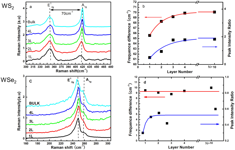
For MX2 layered compounds, there are generally four Raman-active modes, namely A1g, E1g, E12g and E22g modes17,18. E1g mode and low energy E22g mode are absent in our measurements due to the forbidden selection rule in the back-scattering geometry and the limited rejection against Rayleigh scattering respectively. The presented study focuses on the in-plane vibrational E12g mode and the out-of-plane vibrational A1g mode. As these two modes are both polarization sensitive, the exciting laser line was tuned to an unpolarized state. Figure 2.a–d present the representative Raman spectra of WS2 and WSe2 slabs with layer number N = 1 to 4 and bulk. In the case of WS2, we observe the E12g mode at ~350 cm−1 and the A1g mode at ~420 cm−1 (Fig. 2.a)19. The E12g mode shows little dependence on the film thickness, while the A1g mode undergoes a blue shift with increasing layer number, showing a lattice stiffening effect as expected when additional layers are added. By examining the frequency differences (Δω) between the E12g mode and A1g mode, the sample thickness could be identified accordingly. As indicated in Fig. 2.b showing the frequency difference as a function of layer number N, we label Δω = 65.5 cm−1, 68.3 cm−1 and 69.2 cm−1 to monolayer, bilayer and trilayer respectively. For slabs composed of four and more layers, Δω converges to the bulk value at around 70 cm−1. Notably, from monolayer to trilayer the A1g peak is roughly 0.5, 1 and 1.8 times the height of the E12g peak (Fig. 2.b), demonstrating that the ratio of the intensity of A1g mode to that of E12g mode could also be used as an indicator of sample thickness. For WSe2, two dominant peaks are observed around 250 cm−1 in various samples from monolayer to bulk (Fig. 2.c). However, little systematic trend could be observed on both the two modes as shown in Fig. 2.d.
Figure 1.
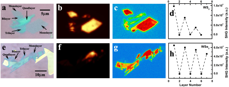
(a) and (e): optical images of WS2 (a) and WSe2 (e) slabs on Si substrates with 300 nm SiO2 cap-layer; (b) and (f): photoluminescence images at direct gap transition energy of the corresponding WS2 (b) and WSe2 (f) slabs excited at 2.41 eV. Only monolayers are visible at the present contrast; (c) and (g): the corresponding SHG under a 800 nm excitation at normal incidence (150 fs, 80 MHZ) on WS2 (c) and WSe2 (g) respectively. The highest intensity labeled in red arises from monolayers. The SHG signal from the silicon/silicon oxide surface is negligible compared with those from multilayers; (d) and (h): The relative intensity of SHG as a function of the film thickness in WS2 (d) and WSe2 (h). The SHG shows an even-odd oscillation dependence on the layer number.
Figure 2.
(a) and (c): Raman spectra of WS2 (a) and WSe2 (c) ultrathin layers; (b) and (d): The frequency difference (red) and the peak intensity ratio (blue) between E12g and A1g modes as a function of film thickness in WS2 (b) and WSe2 (d) respectively.
An experimental method to examine the inversion symmetry in ultrathin film is to study the nonlinear optical effect such as SHG determined by the second order susceptibility χ(2) 20. In the presence of inversion symmetry, χ(2) is zero. A dramatic even-odd oscillation pattern is indeed observed on the SHG intensity consistent with the presence (absence) of inversion symmetry in even-layer (odd-layer) as shown in Fig. 1.c and 1.g. WS2 and WSe2 ultrathin slabs are scanned by a 150 fs pulsed laser beam with a wavelength of 800 nm at normal incidence and the signal at the double frequency (400 nm) is collected. As expected, in both WS2 and WSe2 slabs with even layer number or bulk samples, negligible SHG are observed as same in the case of the bare substrate (SiO2 on Si), and strong second harmonic emission arises from multilayer slabs with odd layer number. Notably, the brightest second harmonic emission is observed in monolayers of both WS2 and WSe2. The intensity of the second harmonic emission decays gradually with the increasing layer number, as indicated in Fig. 1.d and 1.h.
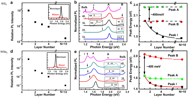
The Photoluminescence study shows that WS2 and WSe2 exhibit a transition from indirect band-gap semiconductor in the form of bulk and multilayers to direct band-gap one in monolayers, similar to MoS27,8,21,22. Figure 3 illustrates the PL spectra of WS2 and WSe2 samples with various thicknesses measured under the same condition with an excitation at 2.41 eV. Fig. 3.a and 3.d show the PL peak intensity as a function of thickness. The PL intensity is found to be extremely weak on bulk samples, consistent with an indirect band-gap semiconductor in bulk form. As WS2 and WSe2 thin to a few atomic layers, the intensity of PL from direct interband transition dramatically increases and reaches maximum at monolayers, more than 3 orders of magnitude stronger than that from bulk. Both WS2 and WSe2 monolayers show much brighter PL with intensity at one order of magnitude higher than bilayers. The peak originating from the indirect band-gap transition (labeled as “I” in Fig. 3.b and 3.e) gradually shifts toward higher energy and fades to null at monolayers. These behaviors are fully consistent with the calculated band structures (see Fig. 4 and supplementary information).
Figure 3.
(a) and (d): The relative PL intensity of WS2 (a) and WSe2 (d) multilayers respectively as a function of film thickness under the same conditions (normalized by the PL intensity of monolayer at 1). Insets present PL spectra from WS2 (a) and WSe2 (d) monolayers and bilayers respectively. The spectra were taken at the same conditions (excitation power, exposure time, etc.); (b) and (e): The normalized PL spectra (with respect to the peak A) of WS2 (b) and WSe2 (e) ultrathin films. I labels the luminescence from indirect gap interband transition, A and B label the direct-gap transitions from the split valence band edge to the conduction band edge at K points (see text). Spectra (dash line) in the zoom windows have been multiplied by a factor as indicated for clarity; (c) and (f): The peak positions of I, A and B transitions as a function of the film thickness in WS2 (c) and WSe2 (f). Both cases show a nearly constant energy difference of ~0.4 eV which corresponds to the splitting of the valence band edge. The universal A-B splitting implies a suppression of interlayer hopping in tungsten dichalcogenides ultrathin thin films.
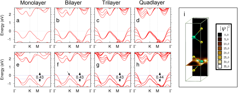
Figure 4. Ab initio calculated band structures for WS2 ultrathin films.
(a–d): without spin-orbit coupling; (e–h): with spin-orbit coupling. The valence band splittings at K point are nearly constants, around 0.43 eV for mono-,bi-, tri, and quad-layers; (i) Electron density map for one valence band Bloch state at K point in WS2 bilayer (indicated by the dashed arrow in (f)). The wavefunction is fully spin polarized in the down state and almost fully localized in the bottom layer. The other degenerate state at the same K point can be obtained by a spatial inversion plus a time reversal operation.
Besides the peaks from indirect transition and the prominent direct transition peak (A), weak PL peak (B) is observed at higher energy in WS2 and WSe2 at all thickness. Note that the similar peak B appearing in MoS2 multilayers is absent in monolayers7. The linewidth of peak A and B implies their excitonic origin as the case in MoS27,23. Strikingly, the splitting between A and B peaks are almost identical, around 0.4 eV for mono-, bi-, tri- and quad-layer samples (see Fig 3.c and 3.f). In monolayers, it is now well understood that the valence band edges at K points have a spin splitting purely arising from the strong spin-orbit coupling in the d-orbitals of the W atom, and we can attribute A and B to the direct-gap transitions between the spin split valence bands and the conduction band at the K points7. However, in multilayers, both the spin-orbit coupling and the interlayer hopping contribute to the valence band splitting at K points. Besides, even layer samples are inversion symmetric while odd layer samples are asymmetric. These in general would result in complex and layer-number dependent splitting patterns in multilayers, which is obviously different from the universal A-B splitting in the PL spectra observed. It implies a novel cause in tungsten dichalcogenides ultrathin thin films.
Discussion
To understand the A-B splitting pattern in WS2 and WSe2 ultrathin films, we perform ab initio calculations of the band structures using the projector augmented wave method24 and generalized gradient approximation25 implemented in the ABINIT code26,27. The structure parameters are taken from Ref. 10. Figure 4.a–d show the band structures of mono-, bi-, tri-, and quad-layer WS2 in the absence of SOC. As expected, the valence band edge at K point splits into two, three, and four bands respectively for bi-, tri-, and quad-layer WS2 due to the interlayer hopping. A hopping matrix element t ~0.1 eV can be extracted from the splitting pattern. However, when spin-orbit coupling (SOC) is included, the splitting pattern is completely changed as shown in Fig. 4.e–h. The valence band edges split into two degenerate manifolds with a splitting magnitude independent of the film thickness for both WS2 and WSe2. The band structures of WSe2 ultrathin films could be found in supplementary information. This is in perfect agreement with the A-B splitting patterns observed in the photoluminescence of mono-, bi-, tri-, and quad-layer WS2 and WSe2. The calculated valence band edge splittings of 0.43 eV in WS2 and 0.47 eV in WSe2 also agree with the measured A-B splitting of 0.4 eV as shown in Fig. 3 and the supplementary information.
In fact, the unexpected splitting patterns in multilayer WS2 and WSe2 are manifestations of the giant spin-valley coupling in valence band9. In monolayers, the Kramer's doublet  and
and  are separated from the other doublet
  and
and  by the spin-valley coupling energy of λsvc ~ 0.4 eV9. In the 2H stacked multilayers, any two neighboring layers are 180 degree in plane rotation of each other. This rotation switches K and K′ valleys but leaves the spin unchanged, which results in a sign change for the spin-valley coupling from layer to layer. Thus, the spin-conserving interlayer hopping can only couple states in neighboring layers with a detuning λsvc. Interlayer hopping is therefore strongly suppressed by the giant spin-valley coupling. A direct consequence is that the splitting patterns remain the same as that of monolayers, and the valence band Bloch states near K points are largely localized in individual layers, as if the interlayer hopping is absent. This is indeed confirmed by ab initio calculations of electron density distributions of these Bloch states (see Fig. 4.i and table S2 in supplementary information). The full suppression of interlayer hopping at K points by the spin-valley coupling is unique to tungsten dichalcogenides where λsvc ≫ t. For molybdenum dichalcogenides where λsvc ~ t, interlayer hopping will manifest in both the splitting pattern and Bloch function28.
The above picture also explains why the hot luminescence peak B can be observable from monolayers to multilayers at an energy much higher than the prominent direct bandgap transition peak A. In monolayers, near K points, the spin-valley coupling gives rise to two non-degenerate valence bands with opposite spin separated by an energy of λsvc ~ 0.4 eV. The relaxation of hot carriers between the spin-split valence bands requires a spin flip and is much slower than intra-band relaxation. Hot carriers can thus have a finite lifetime at the higher energy band edge, giving rise to hot luminescence, i.e. the direct bandgap transition peak B8. In multilayers, we have the same picture for hot carrier relaxation and hot luminescence at the valence band edges near K points where interlayer hopping is fully suppressed by the spin-valley coupling. The giant spin-valley coupling offers a new strategy to manipulate electron spin and makes tungsten dichalcogenides ultrathin films promising materials for semiconductor based spintronics and conceptual valley-based electronics.
Methods
WS2 and WSe2 flakes were mechanically exfoliated from synthesized single crystal bulk samples onto silicon wafers capped with a 300 nm thick SiO2 by a method analogous to the way of producing graphene1. WS2 and WSe2 slabs were first visually screened with interference color through optical microscope. Typical optical images of WS2 and WSe2 ultrathin slabs are presented in Fig. 1.a and 1.e. The film thickness is confirmed by atomic force microscope. PL spectra are also used as an indicator of monolayer samples (Fig. 1.b and 1.f). Raman scattering was carried out with a confocal setup.
Author Contributions
X.C. and H.Z. designed the experiments. X.Chen. and Y.Y. fabricated the single crystal WS2 and WSe2, H.Z., J.D., B.Z., R.H. and L.X. performed the experiments. W.Y. and G.L. contributed to the theoretical interpretations and ab initio calculations. All authors discussed the results and co-wrote the paper.
Supplementary Material
Supplementary Information
Acknowledgments
We thank Mr. Xiaohu Wang, Dr. Changcheng Zheng and Dr. Helen Leung for technique assistance. J.D. acknowledges the financial support from National Natural Science Foundation of China (#11204184). The work was supported by University Grant Council (AoE/P-04/08) and the Research Grant Council (HKU706412P) of the government of Hong Kong SAR and the National Basic Research Program of China (973 Program, Grant No. 2012CB922002).
References
- Novoselov K. S. et al. Electric Field Effect in Atomically Thin Carbon Films. Science 306, 666–669 (2004). [DOI] [PubMed] [Google Scholar]
- Novoselov K. S. et al. Two-dimensional atomic crystals. Proceedings of the National Academy of Sciences of the United States of America 102, 10451–10453 (2005). [DOI] [PMC free article] [PubMed] [Google Scholar]
- Coleman J. N. et al. Two-Dimensional Nanosheets Produced by Liquid Exfoliation of Layered Materials. Science 331, 568–571 (2011). [DOI] [PubMed] [Google Scholar]
- Podzorov V., Gershenson M. E., Kloc C., Zeis R. & Bucher E. High-mobility field-effect transistors based on transition metal dichalcogenides. Applied Physics Letters 84, 3301–3303 (2004). [Google Scholar]
- Radisavljevic B., Radenovic A., Brivio J., Giacometti V. & Kis A. Single-layer MoS2 transistors. Nat Nano 6, 147–150 (2011). [DOI] [PubMed] [Google Scholar]
- Fang H. et al. High-Performance Single Layered WSe2 p-FETs with Chemically Doped Contacts. Nano Letters 12, 3788–3792 (2012). [DOI] [PubMed] [Google Scholar]
- Mak K. F., Lee C., Hone J., Shan J. & Heinz T. F. Atomically Thin MoS2: A New Direct-Gap Semiconductor. Physical Review Letters 105, 136805 (2010). [DOI] [PubMed] [Google Scholar]
- Splendiani A. et al. Emerging Photoluminescence in Monolayer MoS2. Nano Letters 10, 1271–1275 (2010). [DOI] [PubMed] [Google Scholar]
- Xiao D., Liu G.-B., Feng W., Xu X. & Yao W. Coupled Spin and Valley Physics in Monolayers of MoS2 and Other Group-VI Dichalcogenides. Physical Review Letters 108, 196802 (2012). [DOI] [PubMed] [Google Scholar]
- Zhu Z. Y., Cheng Y. C. & Schwingenschlögl U. Giant spin-orbit-induced spin splitting in two-dimensional transition-metal dichalcogenide semiconductors. Physical Review B 84, 153402 (2011). [Google Scholar]
- Xiao D., Yao W. & Niu Q. Valley-Contrasting Physics in Graphene: Magnetic Moment and Topological Transport. Physical Review Letters 99, 236809 (2007). [DOI] [PubMed] [Google Scholar]
- Yao W., Xiao D. & Niu Q. Valley-dependent optoelectronics from inversion symmetry breaking. Physical Review B 77, 235406 (2008). [Google Scholar]
- Cao T. et al. Valley-selective circular dichroism of monolayer molybdenum disulphide. Nat Commun 3, 887 (2012). [DOI] [PMC free article] [PubMed] [Google Scholar]
- Zeng H., Dai J., Yao W., Xiao D. & Cui X. Valley polarization in MoS2 monolayers by optical pumping. Nat Nano 7, 490–493 (2012). [DOI] [PubMed] [Google Scholar]
- Mak K. F., He K., Shan J. & Heinz T. F. Control of valley polarization in monolayer MoS2 by optical helicity. Nat Nano 7, 494–498 (2012). [DOI] [PubMed] [Google Scholar]
- Sallen G. et al. Robust optical emission polarization in MoS2 monolayers through selective valley excitation. Physical Review B 86, 081301 (2012). [Google Scholar]
- Verble J. L. & Wieting T. J. Lattice Mode Degeneracy in MoS2 and Other Layer Compounds. Physical Review Letters 25, 362–365 (1970). [Google Scholar]
- Molina-Sánchez A. & Wirtz L. Phonons in single-layer and few-layer MoS2 and WS2. Physical Review B 84, 155413 (2011). [Google Scholar]
- Ramakrishna Matte H. S. S. et al. MoS2 and WS2 Analogues of Graphene. Angewandte Chemie International Edition 49, 4059–4062 (2010). [DOI] [PubMed] [Google Scholar]
- Shen Y. R. Principles of nonlinear optics. (1984). [Google Scholar]
- Li T. & Galli G. Electronic Properties of MoS2 Nanoparticles. The Journal of Physical Chemistry C 111, 16192–16196 (2007). [Google Scholar]
- Lebègue S. & Eriksson O. Electronic structure of two-dimensional crystals from ab initio theory. Physical Review B 79, 115409 (2009). [Google Scholar]
- Korn T., Heydrich S., Hirmer M., Schmutzler J. & Schuller C. Low-temperature photocarrier dynamics in monolayer MoS2. Applied Physics Letters 99, 102109 (2011). [Google Scholar]
- Torrent M., Jollet F., Bottin F., Zérah G. & Gonze X. Implementation of the projector augmented-wave method in the ABINIT code: Application to the study of iron under pressure. Computational Materials Science 42, 337–351 (2008). [Google Scholar]
- Perdew J. P., Burke K. & Ernzerhof M. Generalized Gradient Approximation Made Simple. Physical Review Letters 77, 3865–3868 (1996). [DOI] [PubMed] [Google Scholar]
- Gonze X. A brief introduction to the ABINIT software package. Zeitschrift für Kristallographie 220, 558–562 (2005). [Google Scholar]
- Gonze X. et al. First-principles computation of material properties: the ABINIT software project. Computational Materials Science 25, 478–492 (2002). [Google Scholar]
- Cheiwchanchamnangij T. & Lambrecht W. R. L. Quasiparticle band structure calculation of monolayer, bilayer, and bulk MoS2. Physical Review B 85, 205302 (2012). [Google Scholar]
Associated Data
This section collects any data citations, data availability statements, or supplementary materials included in this article.
Supplementary Materials
Supplementary Information


