Abstract
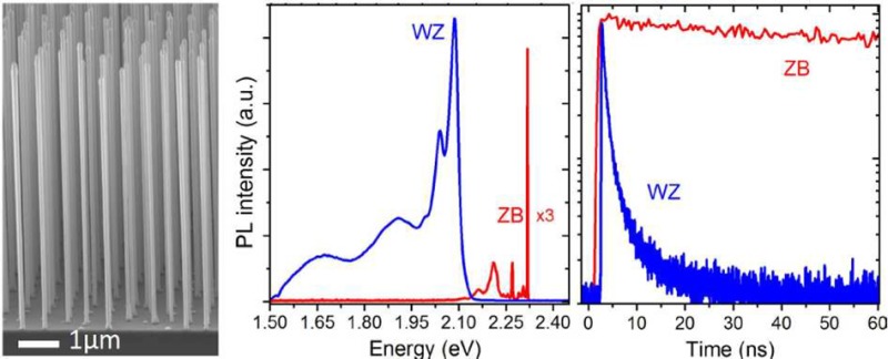
The main challenge for light-emitting diodes is to increase the efficiency in the green part of the spectrum. Gallium phosphide (GaP) with the normal cubic crystal structure has an indirect band gap, which severely limits the green emission efficiency. Band structure calculations have predicted a direct band gap for wurtzite GaP. Here, we report the fabrication of GaP nanowires with pure hexagonal crystal structure and demonstrate the direct nature of the band gap. We observe strong photoluminescence at a wavelength of 594 nm with short lifetime, typical for a direct band gap. Furthermore, by incorporation of aluminum or arsenic in the GaP nanowires, the emitted wavelength is tuned across an important range of the visible light spectrum (555–690 nm). This approach of crystal structure engineering enables new pathways to tailor materials properties enhancing the functionality.
Keywords: Semiconductor nanowires, gallium phosphide, wurtzite, direct band gap, photoluminescence
Widely used semiconductors like germanium (Ge) and gallium phosphide (GaP) have an indirect band gap for the normal cubic (diamond or zinc blende) crystal structure,1 severely limiting their use for light-emitting devices.2,3 Band structure calculations, however, predict a direct band gap for these materials when they have the hexagonal (wurtzite) crystal structure.4−8 A unique feature of the vapor–liquid–solid (VLS) nanowire growth mechanism is that well-known semiconductors can be grown with different crystal structures.9−14 The calculated direct band gap energy for wurtzite GaP ranges between 2.18 and 2.25 eV6,7 and therefore is a promising candidate for light emission in the green-yellow region of the visible spectrum. Similarly, the band gap of aluminum phosphide (AlP) is predicted to change from indirect to direct when the structure is converted from cubic to hexagonal with gap energy of 2.97 eV.6 Therefore, by forming ternary AlxGa1–xP and GaAsyP1–y compounds, the emission wavelength can theoretically be tuned over a wide range. The transition from indirect to a direct band gap by changing from zinc blende to wurtzite has not yet been demonstrated experimentally for any material at ambient pressure conditions.
For this study, GaP nanowires are grown on (111) oriented zinc blende GaP substrates using the VLS mechanism and patterned gold islands as catalysts at a temperature of 750 °C and low V/III ratio to promote the formation of the wurtzite crystalline structure9−14 (see Supporting Information S1 for more details). In order to control the nanowire position two lithography techniques are used; electron beam lithography to fabricate small arrays with varying pitch and diameter,15 and nanoimprint to pattern large-scale areas with a constant pitch and diameter. The cross sectional scanning electron microscopy (SEM) image in Figure 1a shows a uniform array of 6.6 ± 0.2 μm long nontapered nanowires with almost 100% yield defined by nanoimprint. An SEM image of e-beam defined nanowire arrays is shown in the Supporting Information Figure S1. Radial growth, which leads to tapered nanowires, has been totally suppressed by using HCl during growth.16 The optical photograph image in Figure 1b shows the large-scale uniformity of a typical sample. The periodicity of the nanoimprint pattern is clearly visible in Figure 1c.
Figure 1.
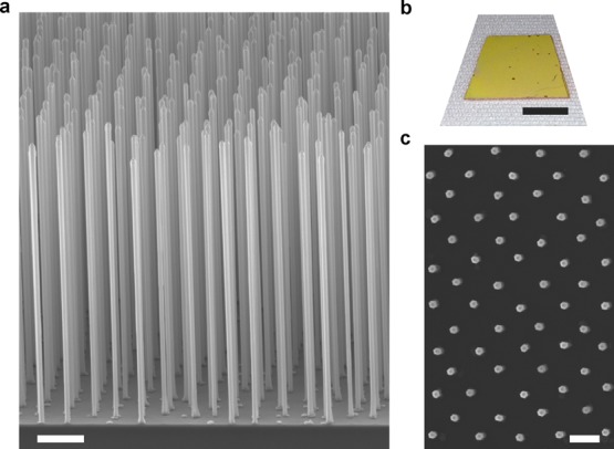
Uniformity of GaP nanowire arrays. (a) SEM picture of GaP/Al0.4Ga0.6P core/shell nanowires in a nanoimprint pattern (tilting angle 70°). Scalebar corresponds to 1 μm. We note that although the wires are grown at high temperatures (T = 750 °C), untapered wires are obtained by the use of HCl during growth. (b) Optical image of the nanowires sample. Scalebar corresponds to 0.5 cm. (c) SEM top-view image of the same sample as in (a) showing the periodicity of the nanoimprint pattern. Scalebar corresponds to 500 nm.
In order to assess the crystal structure of the nanowires, high-resolution transmission electron microscopy (HRTEM) studies are performed. The TEM image in Figure 2a and the corresponding fast Fourier transform (Figure 2b) demonstrate the wurtzite crystal structure of the GaP nanowires. Typically, less than 1 stacking fault per micrometer is observed for the tens of wires studied. An example of a whole wire, which has been imaged from top to bottom by TEM is shown in the Supporting Information Figure S2. A wider band gap ternary AlGaP shell is grown around the GaP17 core to suppress possible undesirable surface effects, as will be discussed below. Shells are grown under different conditions compared to axial nanowire growth, and the thickness is controlled by the shell growth time and the composition by the Al/Ga gas input ratio. The core/shell structure is visible from the high-angle annular dark field (HAADF) TEM image in Figure 2c and the shell composition and thickness for the different samples have been determined from energy-dispersive X-ray (EDX) line scans as shown in Figure 2d. We observe rotation of the side facets during the AlGaP shell growth. As a result of this, the projected thickness of the shell varies across the nanowire producing a small “bump” in the EDX profile (see Supporting Information Figure S2e for more details). This particular wire has a 10 nm thick Al0.4Ga0.6P shell (Supporting Information Figure S2f). Important to mention is that AlGaP is nearly lattice matched to GaP,1 and as a result no defects are generated in the shell.
Figure 2.
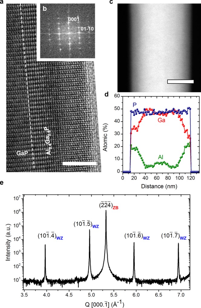
Structural properties of wurtzite GaP nanowires. (a) HRTEM image showing the pure wurtzite crystal structure. The Al0.4Ga0.6P shell lattice matches the core and no defects are nucleated from the interface. The scalebar corresponds to 5 nm. (b) FFT image of the GaP nanowire in (a). (c) HAADF TEM image of a GaP/Al0.4Ga0.6P core/shell wire, showing the uniformity of the shell. The scalebar corresponds to 50 nm. (d) EDX line scan taken perpendicular to the nanowire axis, showing the GaP/Al0.4Ga0.6P core/shell structure. (e) X-ray diffraction intensity along the crystal truncation rod through the (2̅2̅4̅) substrate peak, which includes the (101̅.l̅) wurtzite peaks. The resolution-limited line widths of the WZ peaks and the absence of signal between the peaks show the high quality of the WZ material.
To check the sample quality and to determine the wurtzite lattice parameters, X-ray diffraction measurements are performed on large area nanowire samples patterned by nanoimprint. In the scan in Figure 2e the (101̅.l̅) peak series for the WZ wires and the (2̅2̅4̅) ZB substrate peak are observed, while no extra peaks from polytype structures (ZB, 4H, 6C) are found (see Supporting Information S2 for more details). This together with the narrow line width of the WZ peaks, which is limited by the resolution of the setup, shows the high crystalline quality of the sample. The measured a- and c- lattice parameters for the WZ unit cell are, respectively, 3.842 and 6.335 Å, which differ from the values when the ZB parameters are geometrically converted into the WZ unit cell. In the wires, the WZ unit cell is elongated along the growth (c-) axis and compressed in the in-plane direction along the a-axes similar to what is found for the WZ phase of other III–V nanowires.18 This increase of the c/a ratio, which measures the hexagonal crystal field, is in agreement with the results of density functional theory (DFT) calculations within the local density approximation (LDA).7 On the basis of these experimental lattice values the electronic band structure is calculated by DFT with the LDA-1/2 method taking quasi-particle corrections and spin–orbit interaction into account. The lowest predicted conduction to valence band transition, Γ9v→Γ8c, corresponds to a band gap value of 2.12 eV.
In order to verify the direct nature of the band gap of WZ GaP, the wires are studied with low-temperature microphotoluminescence (PL). For this, e-beam defined nanowire array samples are used with a wire-to-wire spacing of 1.0 μm. The emission intensity and radiative lifetime of the WZ nanowires are compared with a ZB (001) bulk GaP sample as a reference. The PL spectrum of the ZB GaP substrate in Figure 3a exhibits two main peaks at 2.317 and 2.268 eV, corresponding to the A-line, which originates from excitonic emission from isoelectronic nitrogen impurities on P lattice sites, and its phonon-replica.19 The GaP/Al0.4Ga0.6P core/shell nanowires show the strongest emission at 2.09 eV (=594 nm) with a full width at half-maximum (FWHM) of 29 meV, together with a wider and less intense peak at 2.04 eV (=607 nm) with a FWHM of 53 meV and two broad emissions at 1.91 and 1.65 eV. Bare WZ GaP nanowires show identical PL spectra, only with slightly lower intensity. To ensure that this emission originates from the wires and not from the substrate, nanowires are transferred from a substrate patterned by nanoimprint into a PDMS20 film coated with a titanium/gold back mirror, yielding similar results. The peak at 2.09 eV agrees with the lowest interband transition, Γ9v→Γ8c, predicted at a value of 2.12 eV. It is known that nitrogen can induce direct transitions in GaP.21,22 Because we can exclude any possible source of atomic nitrogen in our reactor, we can rule out nitrogen related direct emission from the nanowires. The peak at 2.04 eV most probably corresponds to a transition from the conduction band to a carbon acceptor level.1 We assign the broad band at 1.91 eV to type II ZB/WZ junctions,18 resulting from the few stacking faults in our samples, which is supported by the theoretically predicted valence band offset of 0.14 eV between ZB and WZ,7 and the band at 1.65 eV to incorporated impurities.19 The integrated PL intensity of the peak at 2.09 eV shows a linear dependence on the excitation power density with a saturation of the curve observed at high excitation powers. The slope of a fitted power law dependence (I ∝ Pk) is 0.8–1.0, indicating that the PL emission is due to excitonic recombination.23 The exciton binding energy is obtained from temperature-dependent PL measurements and is 11 ± 4 meV. The energy gap at T = 0 K is extracted to be between 2.09 and 2.11 eV.
Figure 3.
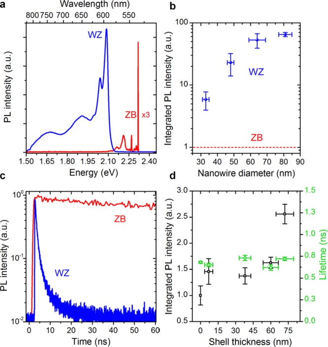
Demonstration of the direct band gap of wurtzite GaP nanowires. (a) Photoluminescence spectra of a ZB (100) GaP substrate (red spectrum) and of WZ GaP/Al0.4Ga0.6P nanowires (blue spectrum). For both spectra, an excitation wavelength of 405 nm at a power of 0.6 W/cm2 is used. (b) Integrated PL emission of the main ZB substrate peak at 2.317 eV (red line) is compared to that of the main WZ wire peak at 2.09 eV for different nanowire core diameters (blue data points). (c) Time-resolved measurements of the samples in (a), showing a fitted lifetime of 254 ns for the ZB substrate and 0.78 ns for the WZ wires, demonstrating the direct nature of the WZ GaP semiconductor material. The same data is shown within a larger time window in the Supporting Information S3. (d) Integrated PL intensity and lifetime of the WZ wire peak at 2.09 eV as a function of the Al0.4Ga0.6P shell thickness. (a–d) All measurements are performed at 4 K.
The spectra in Figure 3a are obtained under identical experimental conditions so that we can quantitatively compare the PL intensity of the WZ wires and that of the ZB substrate. In Figure 3b, the integrated PL emission of the main ZB peak at 2.317 eV is compared to that of the main WZ wire peak at 2.09 eV for different wire diameters. The WZ PL intensity increases with wire diameter, due to increased volume, and levels off at the largest diameters. It is important to note that the integrated PL emission of WZ wires (80 nm diameter) is 65 times higher than that of the ZB GaP(001) substrate. This represents a lower limit of the enhancement factor of the WZ PL intensity, since this value is not corrected for the probed materials volume. Note that the wires cover less than 1% of the surface area, and moreover, the in and out coupling of light from the microscope objective is much better for a planar substrate compared to vertical nanowires.24 We have used a high quality ZB GaP(001) substrate as a reference, since the phonon assisted band-to-band emission of a GaP(111) substrate, observed at 2.28 eV at higher excitation power, is below the detection limit under these measurement conditions. The high emission intensity, the excitonic nature of the emission, together with the very good agreement between the experimental and predicted WZ GaP band gap values strongly suggest the presence of direct band gap transitions in the WZ GaP nanowires.
To further substantiate the direct nature of the band gap, we perform time-resolved PL measurements on WZ GaP/Al0.4Ga0.6P core/shell nanowires as well as on ZB bulk GaP (Figure 3c). A long lifetime of 254 ± 3 ns is obtained for the A-line of the ZB bulk GaP (the full decay curve is shown in Supporting Information Figure S5), which is in the typical range for an indirect band gap transition. In strong contrast, a lifetime of 0.78 ± 0.01 ns is observed for the WZ core/shell nanowires (fit is shown in Supporting Information Figure S5), which compares favorably to lifetimes reported for direct band gap semiconductor like GaAs.25 The striking difference in lifetimes marks the transition from indirect to direct band gap material by transforming the crystal structure from ZB to WZ.
In order to rule out any surface-related decay process, we have studied the PL intensity and lifetime of core/shell nanowires as a function of the Al0.4Ga0.6P shell thickness. Figure 3d shows that a thin shell (7 nm) increases the PL intensity by a factor of 1.5, but increasing the shell thickness further (up to 60 nm) has no major effect on the intensity. The small increase of the intensity indicates that surface states have only a minor effect on the optical properties of the wires. The intensity increase for the thickest shell of 72 nm is explained by enhanced absorption/emission of the wire, since the lifetime is unaffected. The temporal evolution of the PL intensity is independent of the shell thickness and the decay time is around 0.8 ns for all samples.
To address the emission tunability across a significant portion of the visible range, WZ AlxGa1–xP and GaAsyP1–y ternary compound nanowires are grown. In Figure 4a, emission spectra of ternary compounds with different compositions are shown. Partial substitution of Ga by Al induces a blueshift of the emission down to 555 nm with an Al concentration of 46%, while substitution of P by As induces a redshift of the emission up to 690 nm with an As concentration of 70%, demonstrating that the emission color can be adjusted for a range of wavelengths, which is important for solid state lighting. The PL lifetime has been determined for the different compositions and Figure 4c shows that the lifetime is between 0.5 and 1 ns for all samples. It is important to mention that the emission intensity and lifetime of GaAsyP1–y ternary nanowires are independent of the As composition, unlike in the case of bulk ZB GaAsyP1–y, which has a direct/indirect energy gap crossover point at a composition of y = 0.57.26 This confirms that these wurtzite ternary nanowires preserve the direct nature of the band structure over the whole compositional range.
Figure 4.
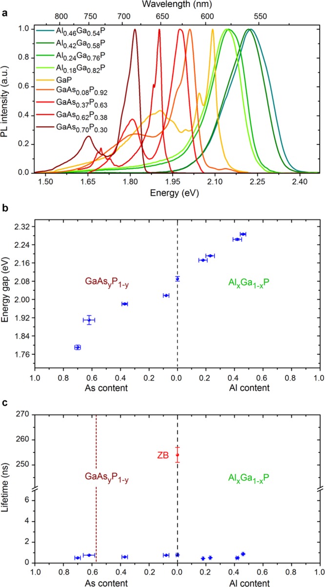
Tunability of the emission wavelength of wurtzite nanowires. (a) Photoluminescence spectra of WZ AlxGa1–xP and GaAsyP1–y ternary compound wires, showing the tunability of the emission wavelength. Substitution of Ga by Al induces a blueshift, and substitution of P by As a redshift of the emission. (b) Energy at the emission maxima as a function of the nanowire composition. (c) Radiative lifetimes as a function of the different wurtzite AlxGa1–xP and GaAsyP1–y compositions (blue data points). The ZB GaP substrate lifetime is at 254 ns (red point). The dotted line at 57% As indicates the direct/indirect transition for zinc blende GaAsP material. All the measurements are performed at 4 K.
We have demonstrated the conversion of indirect band gap semiconductors into direct semiconductors by tailoring the crystal structure. This approach is shown here for GaP and AlP, and by transferring the crystal structure epitaxially14 it can be tested for a variety of other materials. It opens new routes to tune the optical properties of well-established materials with inherent applications. Wurtzite GaP may help to bridge the green gap and increase the efficiency of white light-emitting diodes (LEDs).3 Currently, these devices have a limited efficiency due to a lack of semiconductor materials, which can efficiently emit green light. There are only few semiconductors with a band gap energy corresponding to green light, and each of these has a specific fundamental problem.3,27−29 The external quantum efficiency (EQE) of green emitting LEDs is around 10%, and the current best solution is to use phosphors to convert blue/UV light into green.29 In addition to this application, GaP and AlP have a small lattice mismatch with Si1 and wurtzite GaP hence facilitates the epitaxial integration of photonic materials into silicon technology with a high-quality hetero interface.
Acknowledgments
The authors thank P. J. van Veldhoven for the technical support in the MOVPE reactor, Y. Cui for the nanoimprint substrate preparation and A. J. Standing for the PDMS transfer, T. Hoang and T.T.T. Vu for the technical support in the optical setup, and N. Akopian for critical reading of the manuscript. We thank the Dutch Organization for Scientific Research (NWO-VICI 700.10.441), the Foundation for Fundamental Research on Matter (FOM), and the Austrian Science Fund (FWF-SFB 25) for financial support. D.K acknowledges the support by the Austrian Academy of Sciences.
Supporting Information Available
Additional figures and information. This material is available free of charge via the Internet at http://pubs.acs.org.
The authors declare no competing financial interest.
Supplementary Material
References
- Semiconductors on NSM; http://www.ioffe.rssi.ru/SVA/NSM/Semicond/ (accessed Dec 20, 2012).
- Paniccia M. Integrating silicon photonics. Nat. Photonics 2010, 4, 498–499. [Google Scholar]
- Nakamura S. Current status of GaN-based solid-state lighting. MRS Bull. 2009, 34, 101–107. [Google Scholar]
- Joannopoulos J. D.; et al. Electronic properties of complex crystalline and amorphous phases of Ge and Si. Density of States and Band Structures. Phys. Rev. B 1973, 7, 2644–2657. [Google Scholar]
- Yeh C.-Y.; et al. Relationships between the band gaps of the zinc-blende and wurtzite modifications of semiconductors. Phys. Rev. B 1994, 50, 2715–2718. [DOI] [PubMed] [Google Scholar]
- De A.; Pryor C. E. Predicted band structures of III-V semiconductors in the wurtzite phase. Phys. Rev. B 2010, 81, 155210. [Google Scholar]
- Belabbes A.; Panse C.; Furthmuller J.; Bechstedt F. Electronic bands of III-V semiconductor polytypes and their alignment. Phys. Rev. B 2012, 86, 075208. [Google Scholar]
- Yeh C.-Y.; et al. Zinc-blende −wurtzite polytypism in semiconductors. Phys. Rev. B. 1992, 46, 10086–10097. [DOI] [PubMed] [Google Scholar]
- Algra R. E.; et al. Twinning superlattices in indium phosphide nanowires. Nature 2008, 456, 369–372. [DOI] [PubMed] [Google Scholar]
- Caroff P.; et al. Controlled polytypic and twin-plane superlattices in III–V nanowires. Nat. Nanotechnol. 2009, 4, 50–55. [DOI] [PubMed] [Google Scholar]
- Shtrikman H.; et al. Method for Suppression of Stacking Faults in Wurtzite III-V Nanowires. Nano Lett. 2009, 9, 1506–1510. [DOI] [PubMed] [Google Scholar]
- Joyce H. J.; et al. Phase Perfection in Zinc Blende and Wurtzite III-V Nanowires Using Basic Growth Parameters. Nano Lett. 2010, 10, 908–915. [DOI] [PubMed] [Google Scholar]
- Dick K. A.; et al. Crystal Phase Engineering in Single InAs Nanowires. Nano Lett. 2010, 10, 3494–3499. [DOI] [PubMed] [Google Scholar]
- Algra R. E.; et al. Crystal Structure Transfer in Core/Shell Nanowires. Nano Lett. 2011, 11, 1690–1694. [DOI] [PubMed] [Google Scholar]
- Borgström M. T.; et al. Synergetic nanowire growth. Nat. Nanotechnol. 2007, 2, 541–544. [DOI] [PubMed] [Google Scholar]
- Borgström M. T.; et al. In situ etching for total control over axial and radial nanowire growth. Nano Res. 2010, 3, 264–270. [DOI] [PubMed] [Google Scholar]
- Murayama M. Chemical trend of band offsets at wurtzite/zinc-blende heterocrystalline semiconductor interfaces. Phys. Rev. B 1994, 49, 4710–7724. [DOI] [PubMed] [Google Scholar]
- Kriegner D.; et al. Unit Cell Structure of Crystal Polytypes in InAs and InSb Nanowires. Nano Lett. 2011, 11, 1483–1489. [DOI] [PubMed] [Google Scholar]
- Alawadhi H.; et al. Indirect transitions, free and impurity-bound excitons in gallium phosphide: A revisit with modulation and photoluminescence spectroscopy. J. Appl. Phys. 1997, 82, 4331. [Google Scholar]
- Standing A. J.; et al. High yield transfer of ordered nanowire arrays into transparent flexible polymer films. Nanotechnology 2012, 23, 495305. [DOI] [PubMed] [Google Scholar]
- Zhang Y.; et al. Optical transitions in the isoelectronically doped semiconductor GaP:N: An evolution from isolated centers, pairs, and clusters to an impurity band. Phys. Rev. B 2000, 62, 4493–4500. [Google Scholar]
- Seo H. W.; et al. Nitrogen-doped gallium phosphide nanowires. Chem. Phys. Lett. 2003, 378, 420–424. [Google Scholar]
- Schmidt T. Excitation-power dependence of the near-band-edge photoluminescence of semiconductors. Phys. Rev. B 1992, 45, 8989–8994. [DOI] [PubMed] [Google Scholar]
- Grzela G.; et al. Nanowire Antenna Emission. Nano Lett. 2012, 12, 5481–5486. [DOI] [PubMed] [Google Scholar]
- Hwang C. J. Lifetimes of free and bound excitons in high-purity GaAs. Phys. Rev. B 1973, 8, 646–652. [Google Scholar]
- Shenyz S.-G.; Fanz X.-Q. Lattice and electronic structure properties of GaAs1–xPx semiconducting alloy. J. Phys.: Condens. Matter 1996, 8, 4369–4379. [Google Scholar]
- Li Y.; et al. Defect-reduced green GaInN/GaN light-emitting diode on nanopatterned sapphire. Appl. Phys. Lett. 2011, 98, 151102. [Google Scholar]
- Desnica U. V. Doping limits in II-VI compounds – challenges, problems and solutions. Prog. Crystal Growth Charact. 1998, 36, 291–357. [Google Scholar]
- Oh J. H.; et al. Highly-efficient, tunable green, phosphor-converted LEDs using a long-pass dichroic filter and a series of orthosilicate phosphors for tri-color white LEDs. Opt. Express 2011, 20, S1. [DOI] [PubMed] [Google Scholar]
Associated Data
This section collects any data citations, data availability statements, or supplementary materials included in this article.


