Abstract
Individual atoms and ions are now routinely manipulated using scanning tunnelling microscopes or electromagnetic traps for the creation and control of artificial quantum states. For applications such as quantum information processing, the ability to introduce multiple atomic-scale defects deterministically in a semiconductor is highly desirable. Here we use a scanning tunnelling microscope to fabricate interacting chains of dangling bond defects on the hydrogen-passivated silicon (001) surface. We image both the ground-state and the excited-state probability distributions of the resulting artificial molecular orbitals, using the scanning tunnelling microscope tip bias and tip-sample separation as gates to control which states contribute to the image. Our results demonstrate that atomically precise quantum states can be fabricated on silicon, and suggest a general model of quantum-state fabrication using other chemically passivated semiconductor surfaces where single-atom depassivation can be achieved using scanning tunnelling microscopy.
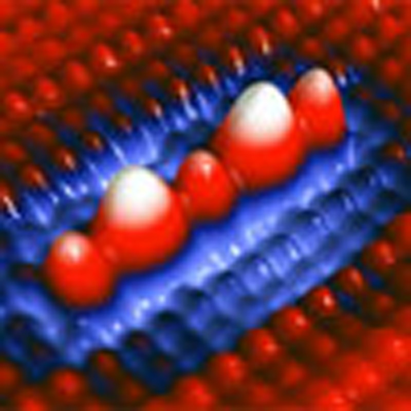 The ability to add and move individual atoms on a surface with a scanning tunnelling microscope enables precise control over the electronic quantum states of the surface. Schofield et al. show that removing hydrogen atoms from a passivated silicon surface can be used to generate and control such states.
One of the great achievements of the last two decades has been the creation and control of quantum states via manipulation of individual atoms. Scanning tunnelling microscopes (STMs) have been used to create quantum-well states on cryogenically cooled metal surfaces1,2, including the celebrated quantum corral, and single ions in electromagnetic traps have been brought together to form coherent systems3. Semiconductors and insulators routinely display defects with clear analogies to ion traps4,5,6,7, and may provide a route toward coupled quantum systems in large numbers as required for applications such as quantum computing8,5,9,10. However, introducing multiple defects deterministically to watch mixed quantum-state formation has proven elusive.
Defects have an enormously important role for semiconductors, from determining electrical conductivity and optical absorption to imposing limits on device performance through the formation of interface trap states11. Defects determine material and device properties because they create localized quantum states that can scatter or bind electrons and holes. A well-known defect in Si is the substitutional impurity from column V of the periodic table, which produces a hydrogenic series of Rydberg states very near the conduction band4,12. In contrast, the dangling bond (DB)—which, in the unreconstructed case, is an sp3 orbital facing a silicon atom vacancy such as would be encountered above a surface, and in bulk is known as the Pb centre—is a deep-centre defect with a bound state that lies well below the conduction band13,14,15,16,17,18. This state is ambiphilic and can be occupied by 0, 1 or 2 electrons corresponding to positive-, neutral- or negative-charge states, respectively.
Here we demonstrate that quantum states can be engineered on silicon for interacting single-atom DB defects. We use an STM to create DBs19,20,14 close enough for wavefunction overlap, but greater than required for bond formation. This results in novel quantum-well1,2,21 states that are fully confined in all dimensions and are highly robust and reproducible. We establish the existence of excited states in the resulting artificial structures, and image them using the STM bias and tip-sample separation as gates.
Results
Isolated DBs
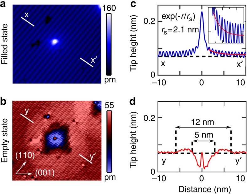
DBs at the surface of Si are particularly interesting because in contrast to most other defects they can be introduced deterministically via STM writing at the atomic scale. This enables the creation of systems of DBs, and we show here that closely spaced DBs can interact to form artificial ‘molecules’ and one- and two-dimensional ‘solids’. The procedure is simple and reproducible: start with a clean Si(001) surface, passivate it with atomic hydrogen, image the surface at low voltage and then desorb selected H atoms using ramps to elevated voltages. Figure 1a shows STM topographs of a single DB ‘atom’ measured with negative and positive sample bias, respectively. Figure 1c shows height profiles across these images. What is immediately apparent is the large extent of the disturbance produced by what one might have thought to be, and what is usually considered as a highly localized object, as well as the qualitatively different appearance for negative and positive voltages. The long-range effects are the result of charge localization at the DB site, which has a strong impact on the images, as the resulting screened Coulomb potentials make the effective bias voltages position dependent.
Figure 1. An isolated DB on an n-type Si(001):H surface.
(a,b) Filled- and empty-state STM images (±1.7 V; 25 pA; 16 × 14 nm2) of a single DB taken at 77 K, with corresponding line profiles shown in c and d. Length measurements have associated uncertainties of ±0.05 nm. The screening length of 2.1 nm calculated from the filled-state image is in agreement with a Thomas–Fermi estimate16. The empty-state image exhibits a ~12 nm diameter enhancement disc due to ionization of the DB and a ~5-nm depression due to non-equilibrium charging of the DB. These features exhibit the expected dependence on the applied bias (see Supplementary Note S1 and Supplementary Fig. S1).
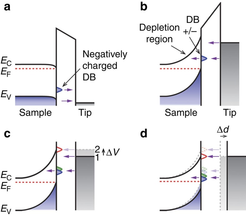
As expected, we observe negatively charged DBs in filled-state images22,23, evident from an extended enhancement that decays with radial distance from the DB (Fig. 1c). However, the charge state of the DB is strongly influenced by the STM tip. It is known that the electric field emanating from the STM tip induces large shifts in the surface energy bands when imaging H-terminated Si(001), such that the Fermi level (EF) of the substrate lies near the conduction/valence band edge under typical filled-/empty-state imaging conditions24,25 as shown in Fig. 2a. However, it is much less well recognized that the consequence for is that empty-state bias the DB ground state will lie above the bulk Fermi level (Fig. 2b), and that under equilibrium conditions this will result in a positively charged DB. We confirm this experimentally by observing the characteristic signature of DBs becoming positively charged under empty-state tunnelling conditions—a sharp-edged disc of increased height surrounding the DB, which has an average diameter of 12 nm in Fig. 1b. The edge of this disc indicates the tip-DB radial separation distance at which the electric field of the STM tip causes the DB to become positively ionized by raising its energy above the bulk EF (Fig. 2b), analogous to recent observations of tip-induced ionization of Si donor atoms in GaAs26. However, DBs on n-type Si(001):H do not remain positively charged as the tip moves closer to them; instead, they again become negatively charged when the tip comes within a certain minimum distance from the DB due to non-equilibrium charging. This is evident by a depression region that surrounds each DB (~5 nm across in Fig. 1b). The STM tip is similar to the gate in a field-effect transistor; a negative tip bias results in an electron depletion region at the surface that decouples the DB from the n-type bulk (Fig. 2b). The DB is then analogous to the island of a single electron transistor, with the tip and substrate forming the source and drain, respectively. Exactly as for a single electron transistor, the electron occupation of the DB is then governed by the electron transfer rates on and off the DB, rather than by equilibrium with the bulk substrate17,27,28,29. Further discussion of this phenomenon, together with data illustrating the bias dependence of the depression and enhancement regions are given in Supplementary Note S1 and Supplementary Fig. S1, respectively. Thus, the DB is negatively charged in both bias polarities when directly imaged with the STM under the measurement conditions shown in this article, and the band alignment and tunnelling processes during DB imaging are well described by Fig. 2a.
Figure 2. Energy-band diagrams for STM imaging of DBs.
(a,b) Filled- and empty-state conditions for a single DB. The DB is negatively charged under filled-state imaging conditions, but can be either negative or positive under empty-state conditions, depending on whether it is in equilibrium with the substrate or not (see text). (c,d) Band diagrams for empty-state imaging of the double DB; its three bound states are indicated as calculated in Fig. 3j. In panel c, two alignments of the tip Fermi level with respect to the surface bands are shown (solid and dashed line), corresponding to two different bias conditions (note: the expected small increase in the band bending in the substrate is not shown in this diagram for clarity). Changing the tunnelling current magnitude and, hence, the tip-sample separation also changes the alignment of the tip and substrate bands; this is illustrated in panel d where two different tip-sample separations are shown by solid and dashed lines. The equivalence of decreasing the tunnelling current and increasing the sample bias is further highlighted in the STM data shown in Supplementary Fig. S3 and discussed in Supplementary Note S3.
DB pair interactions
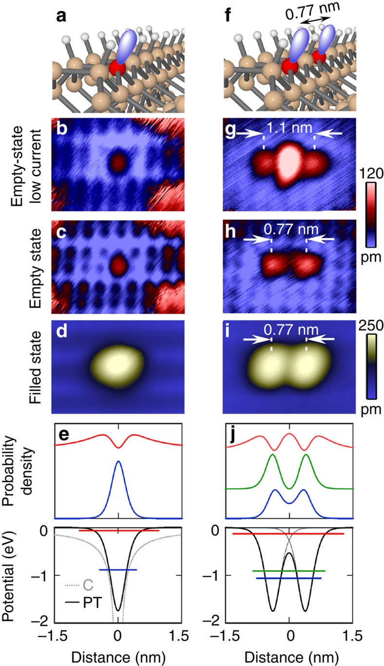
Having established the general mode of imaging individual DBs, we are now in a position to discuss the quantum bound states supported by our manufactured (by STM writing) DB defects. Figure 3 shows high-resolution STM images of a single DB (Fig. 3b–d) and a DB ‘molecule’ consisting of a pair of DBs on next-nearest neighbour lattice sites (Fig. 3g–i), with varying current and voltage settings as indicated. In all images except for Fig. 3g, the DBs present localized protrusions with radii <0.5 nm located at the sites of the missing H atoms. However, when the double DB is imaged in empty states with a very low current set point (5 pA; Fig. 3g), its appearance changes dramatically. In particular, a third, prominent protrusion, reminiscent of a molecular bonding orbital but with much larger spatial extent, occurs between the location of the two missing H atoms, and the separation between the two outer protrusions increases from 0.77 (the next-nearest neighbour distance) to 1.1 nm.
Figure 3. Bound states of single and paired DBs.
(a,f) Ball and stick models (perspective view) of a single DB, and two next-nearest neighbour DBs. (b–d) STM images of a single DB, recorded at +2 V, 5 pA; +2 V, 100 pA; and −2 V, 50 pA, respectively. (g–i) STM images of next-nearest neighbour DBs under similar imaging parameters to the corresponding single-DB images (+2 V, 5 pA; +2 V, 95 pA; and −2 V, 95 pA, respectively). All STM images 3 × 2 nm2. Length measurements have associated uncertainties of ±0.05 nm. (e,j) Probability distributions of the bound states of the single- and double-DB wells, and the potential wells used to generate them. The energy levels for each of the bound states (single DB: −0.95 and −0.02 eV; double DB: −1.07, −0.88 and −0.07 eV) are indicated by horizontal lines on the potential well. A Pöschl–Teller (PT) potential  is used for the single DB, and the double DB is modelled by the addition of two such PT wells separated by 0.77 nm. The single well fits within the surface Coulomb (C) potential (−e2/4πεr); a lower bound to the true potential. Parameters: α=0.24 nm, λ=2.2 and ε=ε0(εb+1)/2, where ε0 and εb are the permitivity of free space and dielectric constant of Si, respectively. Note that the calculations indicate that the STM images in panels g and h correspond to the situations represented, respectively, by the solid and dashed lines in Fig. 2d.
We can understand these data by considering the bound-state probability distributions of the DB potential well(s). The localized protrusions in Fig. 3b–d are all in agreement with the ground-state probability density of a radially symmetric potential well or linear combinations of such states. However, this is not true of the three-lobed feature seen in Fig. 3g; here the maximum in the bound-state intensity occurring at the midpoint between the two missing H atoms requires a contribution from a higher-energy bound state. We confirm this by creating a model potential30 for the single DB that supports two bound states: a ground state near the valence band maximum, consistent with the electron paramagnetic resonance data13 and our density functional theory calculations (that are presented in Supplementary Note S2, Supplementary Table S1 and Supplementary Fig. S2), and a first excited state near the conduction band maximum, as shown in Fig. 3e. Bound-state wavefunctions and energies are obtained via a piecewise continuous solution of the Schrödinger equation (see Methods for further details). When coupled to a second identical well 0.77 nm away, the ground state splits into symmetric and anti-symmetric combinations separated by ~0.2 eV (Fig. 3j). As expected, the probability distributions of the states for the single and double-DB wells (blue and green traces in Fig. 3e) are in good agreement with the STM images in Fig. 3b–d. The wavefunction overlap of the single-well excited state leads to a new state with a probability density maximum located at the midpoint between the two DB sites, and two outer protrusions of lower intensity separated by 1.3 nm (red trace in Fig. 3j), closely resembling the feature we see in the experimental STM data in Fig. 3g. This state can be considered as an excited molecular orbital of the double-DB system. However, we will refer to this state in the following as the low binding energy (LBE) state to avoid ambiguity regarding the electron occupancy of the states. The LBE state is imaged only under certain conditions because of the alignment between the surface and tip energy bands, which is determined by the gating effect of the tip on the substrate. Figure 2c shows an energy-band diagram for imaging the double DB in empty states, which is similar to Fig. 2b but explicitly includes all three of the double-DB bound states (compared with Fig. 3j). The tip EF is drawn with two different alignments to the surface bands. When aligned as in configuration 1, the electrons cannot access the LBE state; the image is then dominated by tunnelling into the conduction band through a small tip-induced depletion region, and transport through the two lower-lying bound states. However, if the tip EF is as shown in configuration 2, then resonant tunnelling through the LBE state will dominate the image. The change in band alignment can be induced by changing the STM tip bias as shown in Fig. 2c, or by changing the tunnelling current set point, which changes the tip-sample separation and, hence, the band bending in the substrate (Fig. 2d). Altering the current also changes the rate of charge transfer to the DB, inducing additional changes to the band alignment and enhancing the effect illustrated in Fig. 2d. In the data shown in Fig. 3g, we have changed the tunnelling current from 5 to 95 pA, such that these images correspond to the solid and dashed lines, respectively, in Fig. 2d.
We note that molecular bonding type states have been reported to form between Mn acceptor atoms in GaAs in the elegant experiments described in ref. 6 and related publications. Although important comparisons can be drawn between the data shown in Fig. 3 and those presented in ref. 6, we stress that there are also important differences. Notably, the states that we describe here are the result of interacting deep-centre defects created through the formation of DBs by the removal of individual hydrogen atoms from a hydrogen-terminated silicon surface. In contrast, the states described in ref. 6 result from the interaction of acceptor states bound to substitutional Mn atoms in a GaAs surface. Moreover, because of the highly localized nature of the defect wavefunctions we create on Si(001):H, we observe significant molecular orbital formation only for the excited states of the individual DB point defects. The ability to fabricate and observe point defects whose ground states are weakly interacting while their excited states couple to form molecular orbitals is particularly interesting. For example, there are quantum-computing proposals that use the excited-state molecular orbitals of systems of hydrogenic impurities in silicon to couple their non-interacting spin ground states9.
DB interactions with varying distance and orientation
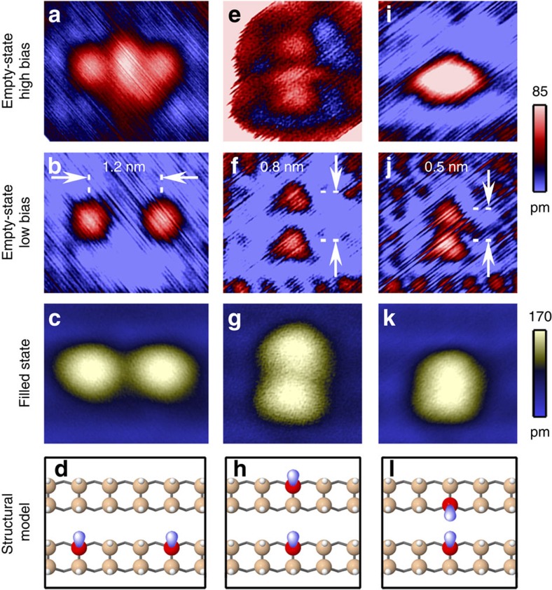
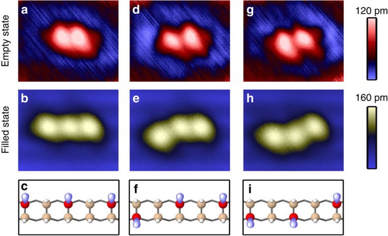
Our ability to write arbitrary combinations of DBs supported by the periodicity of the underlying crystal lattice, together with control of the bias voltage and tip-sample separation permit the creation and observation of engineered quantum states. We have observed similar LBE states for various combinations of DB pairs, including pairs separated by an additional Si dimer (1.15 nm separation, Fig. 4a-d), pairs perpendicular to the dimer rows separated by a single H-terminated Si atom (Fig. 4e-h) and pairs separated only by the dimer trough (Fig. 4i-l). The behaviour of these structures with changing imaging parameters is in agreement with the band alignment model presented above, and the data presented for the DB pair in Fig. 3. We have also created and imaged DBs aligned diagonally across dimer rows; Fig. 5 shows a series of STM images of a three-DB chain in one linear (Fig. 5a–c) and two separate ‘kinked’ configurations (Fig. 5d–f, respectively). The filled-state images resolve three protrusions at the locations of the missing H atoms, whereas the high-bias empty-state images reveal protrusions located between the missing H atoms, consistent with the DB pair data presented above and the extended DB chain data to be presented below (Fig. 6). In the linear configuration, all of the DBs are lined up along one side of a dimer row. However, imaging this structure at elevated bias and current (±2.1 V and 25 pA) caused the leftmost DB to move to the opposite side of the dimer row (that is, the H atom of the Si–Si–H hemihydride dimer shifted from one side of the dimer to the other). This then produced a ‘kinked’ three-DB structure, which is shown in Fig. 5d–f. Subsequently, imaging this structure again with elevated bias and current caused the middle DB to also switch to the opposite side of the dimer row (Fig. 5g–i). Observing the empty-state images in Fig. 5a, we notice a slightly reduced size in the protrusion that occurs between the DB separated diagonally across the dimer row, and a distinct angular appearance consistent with the formation of a molecular orbital between diagonally separated DBs.
Figure 4. DB pairs with varying separation and orientation.
(a–d) Along a dimer row separated by two H-terminated lattice sites (1.9, 1.5, −1.5 V; 5 pA; 2.7 × 2.3 nm2); (e–h) across two dimer rows separated by a single H-terminated lattice site (2.2, 1.7, −2.0 V; 2 pA; 1.9 × 2.3 nm2); and (i–l) on adjacent sites across the dimer trough (2.0, 1.5, −2.0 V; 5 pA; 1.9 × 2.3 nm2). In each case, there is agreement with the behaviour of the DB pair described in Fig. 3; in particular, we see the formation of a protrusion between DB sites at high empty-state bias and low-tunnelling current due to the band alignment between the tip Fermi level and LBE of the DB structures as described in the text. Length measurements have associated uncertainties of ±0.1 nm. Panels d, h and l show top-view schematic ball and stick models for each configuration; silicon atoms with DBs are coloured red.
Figure 5. Three DBs in linear and kinked configurations.
(a–c) Linear arrangement of three DBs on next-nearest neighbour lattice sites (0.77 nm separation between DBs). (d–f) The same chain after the left DB was induced to move to the opposite side of the dimer row by STM stimulation. (g–i) The same chain after the middle of the three DBs was also induced to move to the opposite side of the dimer row. Image parameters are (a,d,g) +2 V, 5 pA; (b,e,h), −1.8 V, 5 pA. Panels c, f and i show top-view schematic ball and stick models for each configuration; silicon atoms with DBs are coloured red.
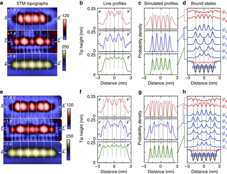
Figure 6. Linear chains of five and six DBs.
(a) STM topographs of the five-DB chain at +1.8, +1.4 and −1.4 V, respectively (15 pA; 4.5 × 2 nm2). (b) Line profiles taken along the DB structures as indicated for each of the images in a. (c) Simulated line profiles generated from linear combinations, Σci|ψi|2, of the individual bound-state solutions to the five-DB system. (d) Five-DB potential well and the probability distributions of its bound-state wavefunctions, ψ1 to ψ7 with binding energies given in eV. (e–h) Repeat of panels a–d for a six-DB chain (images are 5.3 × 2 nm2). The coefficients ci were calculated using ci=e−Ei/α where α=0.15 and 0.3 for filled and empty states, respectively, and Ei is the binding energy of the i-th state. For the low empty-state bias (+1.4 V) simulation of the five-DB, only contributions from ψ4 and ψ5 were included, whereas for the six-DB states ψ5, ψ6 and ψ7 were included with c7=1.5c6 (see text).
DB-extended chains
We have also created more complex arrays, including multiple DBs—the initial steps towards the formation of one-dimensional extended states in analogy to the formation of bulk electronic bands of a solid. Figure 6a shows STM images and height profiles of five- and six-DB chains for imaging paradigms similar to those used to obtain the STM data in Fig. 3 and Fig. 4. We observe that both the filled-state and the low-bias empty-state images (±1.4 V) produce protrusions at the sites of each of the five missing H atoms, consistent with linear combinations of a single-well ground state. The high-bias empty-state images, in contrast, have maxima between the locations of the missing H atoms, suggesting a contribution from LBE states in analogy with the rationale discussed above for the double-DB system.
Simulations of the chains produce the level splitting and wavefunctions expected by symmetry: The ground state of the single DB well splits into five and six states, respectively, for the five- and six-DB structures. Both structures exhibit only two LBE states, as the expected higher-energy combinations lie above the ionization potential. Linear combinations of these states provide remarkable likenesses of the STM data as seen by comparing Fig. 6b with 6c, and Fig. 6f with 6g, . Consider the two filled-state images and corresponding line profiles (green traces in Fig. 6b). We expect these features to be reproduced by the probability densities of the five (six) lowest-lying states in each case (blue traces in Fig. 6d). An equal weighting of these states produces five (six) peaks of equal height in reasonable agreement with the data; however, a better fit to the data, which includes the observed increased intensity towards the centre of the chains, is obtained when we include the effect of the tunnelling matrix element by applying a greater weight to states closer to the sample Fermi level (see discussion in Supplementary Note S1). When imaging empty states at high bias (+1.8 V), we expect the image to be dominated by resonant tunnelling through the LBE states; analysis confirms this and the experimental height profiles are well reproduced by a superposition of the LBE state probability distributions for both the five- and six-DB structures (red traces in Fig. 6b). As the empty-state bias is reduced, the contribution to the image from the LBE states dimishes as indicated schematically in Fig. 2c; for the five-DB structure, we find that the LBE states no longer contribute to the image at +1.4 V and the image is reproduced by a superposition of the next two lowest-energy states (ψ4 and ψ5). The lower-lying ψ1 to ψ3 states are not imaged because of the mechanism of charge transport through these states. The behaviour of the six-DB structure when imaged at +1.4 V is similar; in this case, there is still a contribution from the lowest-energy LBE state due to a slight difference in the overall alignment between the surface and tip energy bands between the five- and six-DB structures. STM images of these five- and six-DB structures taken at a range of biases between +1.4 and +1.8 V, and with both 5 and 15 pA tunnelling current are given in Supplementary Fig. S3, with corresponding text in Supplementary Note S3. These data further illustrate the transition between images dominated by ground- and excited-state orbitals, and they demonstrate the equivalence of decreasing tunnelling current and increasing bias voltage that was described in Fig. 2.
Discussion
We note that the precise shape of the potential well of a deep level defect is in general not known and is difficult to determine either experimentally or theoretically30. Nevertheless, given the model potential in Fig. 3e, we have been successful in qualitatively describing the non-trivial charge distributions of systems of interacting DBs and their complex dependence on both bias voltage and tip height. Furthermore, although increasing the bias and decreasing the tip-sample separation have the same effect on the alignment between the sample and tip energy bands, they have opposite gating effect on the substrate. This confirms the band-alignment picture shown in Fig. 2 as the origin of the changing appearance of the STM images, and excludes a more complicated effect where the nature of the bound states themselves are altered because of a change in the underlying shape of the quantum well.
The data presented above demonstrate the viability of atomic-scale quantum engineering on the Si(001) surface through the creation of systems of interacting DBs. The observation of excited states in these systems is unexpected and provides new insight into the electronic properties of atomic-scale defects in semiconductors. Furthermore, our experiments demonstrate the creation of coherent spatial distributions of wavefunctions complementing recent work in the time domain for hydrogenic defect states in silicon4, where orbitals cannot be directly imaged, as well as work in modern atomic physics3. Future experiments will focus on two-dimensional arrangements of DBs and the inclusion of one or more group V donor atoms31 into the DB structures to alter the wavefunction symmetry (in analogy to the role of nitrogen in the diamond nitrogen vacancy centre5). The method may be applied to any surface, including graphene32, which can be modified by chemical passivation and depassivation.
Methods
Scanning tunnelling microscopy
We performed the experiments using an Omicron LT-STM system operated at 77 K. STM tips were prepared by electrochemically etching 0.25 mm diameter polycrystalline W wire and a combination of electron-beam annealing and field emission in vacuum. Samples were cleaved from 0.05±0.01 Ω cm (room temperature resistivity) Sb-doped wafers (Virginia Semiconductor Inc.) and prepared in vacuum by flash annealing to 1,200 °C. We then hydrogen-terminated the samples using a Tectra atomic hydrogen source while counter heating the substrate to ~400 °C. H atoms were desorbed from the Si(001):H surface19 by positioning the tip above the atom to be desorbed and performing a controlled voltage ramp from +2 to +4 V, with the feedback loop switched off.
Modelling DBs
The localized protrusions in STM images of DBs reflect the bound-state probability distributions, resulting from their defect potential wells16. Unlike the case for hydrogenic impurity states where the functional form of the defect potential well is known (that is, Coulombic), in general, we do not know the functional form of the potential wells of deep-centre defects30. Nevertheless, we can gain insight into the essential underlying physics of deep-centre defects, such as DBs and systems of interacting DBs by numerically solving the Schrödinger equation using piecewise continuous representations of a model potential33. To describe a single DB, it is reasonable to choose any smooth continuous function that produces a highly localized ground state (roughly equal to the interatomic spacing, as observed in experiment), and for which the Coulomb potential, scaled by an appropriate dielectric constant, is lower bound (Fig. 3). Because of the existence of known analytical solutions for its bound-state energies, we choose to represent a single DB using a Pöschl–Teller potential, 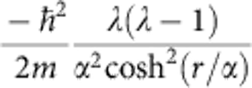 , where ħ is the reduced Planck constant and m is the electron mass. The width and depth of the well are determined by α and λ; we use α=0.24 nm and λ=2.2, which produces a ground state at −0.95 eV and an excited state at −0.02 eV (Fig. 3); that is, just above the valence band maximum and beneath the conduction band minimum, respectively. Similar results would also be obtained with other potentials of the same general form. For systems of interacting DBs, we create the multi-well potential through the addition of individual wells placed at the appropriate spacings; that is, 0.77 nm spacing for the next-nearest neighbour DBs modelled in this work. The values of α and λ are kept fixed at α=0.24 nm and λ=2.2 in all cases. The multi-DB systems are modelled in one dimension corresponding to the symmetry axis through the DBs, providing intuitive solutions that illustrate the essential underlying physics of these multiple DB systems.
Author contributions
S.R.S., C.F.H., N.J.C. and G.A. initiated this work. S.R.S. performed the experiments, data analysis and numerical modelling. D.R.B. performed the DFT calculations. All authors contributed to data interpretation and paper writing.
Additional information
How to cite this article: Schofield, S. R. et al. Quantum engineering at the silicon surface using dangling bonds. Nat. Commun. 4:1649 doi: 10.1038/ncomms2679 (2013).
Supplementary Material
Supplementary Figures S1-S3, Supplementary Table S1, Supplementary Notes 1 and 2, Supplementary Methods and Supplementary References
Acknowledgments
S.R.S. is grateful for conversations with A.J. Fisher, P.T. Greenland, S.A. Lynch, P. Moriarty, G. Morley and A.M. Stoneham. We acknowledge financial support from the Engineering and Physical Sciences Research Council (Career Acceleration Fellowship EP/H003991/1 and COMPASSS EP/H026622/1).
References
- Crommie M. F., Lutz C. P. & Eigler D. M. Confinement of electronics to quamntum corrals on a metal surface. Science 262, 218–220 (1993). [DOI] [PubMed] [Google Scholar]
- Nilius N., Wallis T. M. & Ho W. Development of one-dimensional band structure in artificial gold chains. Science 297, 1853–1856 (2002). [DOI] [PubMed] [Google Scholar]
- Häffner H., Roos C. & Blatt R. Quantum computing with trapped ions. Phys. Rep. 469, 155–203 (2008). [Google Scholar]
- Greenland P. T. et al. Coherent control of Rydberg states in silicon. Nature 465, 1057–1061 (2010). [DOI] [PubMed] [Google Scholar]
- Weber J. R. et al. Quantum computing with defects. Proc. Natl Acad. Sci. USA 107, 8513–8518 (2010). [DOI] [PMC free article] [PubMed] [Google Scholar]
- Kitchen D., Richardella A., Tang J. -M., Flatté M. E. & Yazdani A. Atom-by-atom substitution of Mn in GaAs and visualization of their hole-mediated interactions. Nature 442, 436–439 (2006). [DOI] [PubMed] [Google Scholar]
- Murdin B. N. et al. Si:P as a laboratory analogue for hydrogen on high magnetic field white dwarf stars. Nat. Commun. 4, 1469 (2013). [DOI] [PubMed] [Google Scholar]
- Kane B. E. A silicon-based nuclear spin quantum computer. Nature 393, 133–137 (1998). [Google Scholar]
- Stoneham A. M., Fisher A. J. & Greenland P. T. Optically driven silicon-based quantum gates with potential for high-temperature operation. J. Phys. Condens. Matter 15, L447–L451 (2003). [Google Scholar]
- Koenraad P. M. & Flatté M. E. Single dopants in semiconductors. Nat. Mater. 10, 91–100 (2011). [DOI] [PubMed] [Google Scholar]
- Queisser H. J. & Haller E. E. Defects in semiconductors: some fatal, some vital. Science 281, 945–950 (1998). [DOI] [PubMed] [Google Scholar]
- Lansbergen G. P. et al. Gate-induced quantum-confinement transition of a single dopant atom in a silicon FinFET. Nat. Phys. 4, 656–661 (2008). [Google Scholar]
- Campbell J. P. & Lenahan P. M. Density of states of Pb1 Si/SiO2 interface trap centers. Appl. Phys. Lett. 80, 1945–1947 (2002). [Google Scholar]
- Haider M. B. et al. Controlled coupling and occupation of silicon atomic quantum dots at room temperature. Phys. Rev. Lett. 102, 046805 (2009). [DOI] [PubMed] [Google Scholar]
- Raza H. Theoretical study of isolated dangling bonds, dangling bond wires, and dangling bond clusters on a H: Si(001)-(2 × 1) surface. Phys. Rev. B 76, 045308 (2007). [Google Scholar]
- Hamers R. J. Characterization of localized atomic surface defects by tunneling microscopy and spectroscopy. J. Vac. Sci. Tech. B 6, 1462–1467 (1988). [Google Scholar]
- Berthe M. et al. Probing the carrier capture rate of a single quantum level. Science 319, 436–438 (2008). [DOI] [PubMed] [Google Scholar]
- Stegner A. R. et al. Electrical detection of coherent 31P spin quantum states. Nat. Phys. 2, 835–838 (2006). [Google Scholar]
- Lyding J. W., Shen T. C., Hubacek J. S., Tucker J. R. & Abeln G. C. Nanoscale patterning and oxidation of H-passivated Si(100)-2 × 1 surfaces with an ultrahigh vacuum scanning tunneling microscope. Appl. Phys. Lett. 64, 2010–2012 (1994). [Google Scholar]
- Hitosugi T. et al. Jahn-Teller distortion in dangling-bond linear chains fabricated on a hydrogen-terminated Si(100)-2 × 1 surface. Phys. Rev. Lett. 82, 4034–4037 (1999). [Google Scholar]
- Sagisaka K. & Fujita D. Quasi-one-dimensional quantum well on Si(100) surface crafted by using scanning tunneling microscopy tip. Appl. Phys. Lett. 88, 203118 (2006). [Google Scholar]
- Radny M. W. et al. Single hydrogen atoms on the Si(001) surface. Phys. Rev. B 76, 155302 (2007). [Google Scholar]
- Piva P. G. et al. Field regulation of single-molecule conductivity by a charged surface atom. Nature 435, 658–661 (2005). [DOI] [PubMed] [Google Scholar]
- McEllistrem M., Haase G., Chen D. & Hamers R. J. Electrostatic sample-tip interactions in the scanning tunneling microscope. Phys. Rev. Lett. 70, 2471–2474 (1993). [DOI] [PubMed] [Google Scholar]
- Feenstra R. M. Electrostatic potential for a hyperbolic probe tip near a semiconductor. J. Vac. Sci. Technol. B 21, 2080–2088 (2003). [Google Scholar]
- Teichmann K. et al. Controlled charge switching on a single donor with a scanning tunneling microscope. Phys. Rev. Lett. 101, 076103 (2008). [DOI] [PubMed] [Google Scholar]
- Nguyen T. H. et al. Coulomb energy determination of a single Si dangling bond. Phys. Rev. Lett. 105, 226404 (2010). [DOI] [PubMed] [Google Scholar]
- Wu S. W., Nazin G. V., Chen X., Qiu X. H. & Ho W. Control of relative tunneling rates in single molecule bipolar electron transport. Phys. Rev. Lett. 93, 236802 (2004). [DOI] [PubMed] [Google Scholar]
- Livadaru L., Pitters J. L., Taucer M. & Wolkow R. A. Theory of nonequilibrium single-electron dynamics in STM imaging of dangling bonds on a hydrogenated silicon surface. Phys. Rev. B 84, 205416 (2011). [Google Scholar]
- Yu P. Y. & Cardona M. Fundamentals of Semiconductors: Physics and Materials Properties 4th edn (Springer (2010). [Google Scholar]
- Schofield S. R. et al. Atomically precise placement of single dopants in Si. Phys. Rev. Lett. 91, 136104 (2003). [DOI] [PubMed] [Google Scholar]
- Sessi P., Guest J. R., Bode M. & Guisinger N. P. Patterning graphene at the nanometer scale via hydrogen desorption. Nano Lett. 9, 4343–4347 (2009). [DOI] [PubMed] [Google Scholar]
- Gilmore R. Elementary Quantum Mechanics in one Dimension Johns Hopkins University Press (2004). [Google Scholar]
Associated Data
This section collects any data citations, data availability statements, or supplementary materials included in this article.
Supplementary Materials
Supplementary Figures S1-S3, Supplementary Table S1, Supplementary Notes 1 and 2, Supplementary Methods and Supplementary References


