Abstract
Periodic and reproducible gold nanocuboids with various matrix dimensions and with different inter-particle gaps were fabricated by means of top-down technique. Rhodamine 6G was used as a probe molecule to optimize the design and the fabrication of the cuboid nanostructures. The electric field distribution for the nanocuboids with varying matrix dimensions/inter-particle gap was also investigated. These SERS devices were employed as biosensors through the investigation of both myoglobin and wild/mutated peptides. The results demonstrate the probing and the screening of wild/mutated BRCA1 peptides, thus opening a path for the fabrication of simple and cheap SERS device capable of early detection of several diseases.
Surface enhanced Raman scattering (SERS), ought to its capability of increasing the Raman sensitivity, when molecules are attached or in close proximity of metal-nanostructures1,2,3,4, is one of the leading techniques for molecular analysis with sensitivity down to single molecule5,6,7. This technique is being employed in various research fields spanning from physics to biology, from engineering to forensic and medical science8,9,10. SERS signal can be promoted by means of localized surface plasmon resonances (LSPRs), which are highly sensitive to the shape and size of resonant nanostructures, inter–particle gap (IPG), dielectric environment and polarization of the incident light11,12,13. Therefore, any variation in the geometrical factors could alter the plasmonic properties of the fabricated device, making reproducibility a fundamental issue.
SERS is an outcome originating from the combination of chemical enhancement, mainly related to the charge transfer between the metal nanostructure and the analyte molecules, together with electromagnetic enhancement (induced by the surface electron oscillation in the structure14,15,16,17,18) which is known to be the main contribution in SERS phenomena19. To achieve high electric field intensity and to acquire significant sensitivity, SERS substrates have been fabricated by means of different techniques: e.g. metal colloid20,21,22,23 and shadow mask deposition24 which are able to provide substantial enhancement but the reproducibility is still an issue25. In order to overcome this drawback, a possible solution is given by the fabrication of periodic nanostructures by means of top-down approaches26,27,28,29,30,31,32 which guarantee high level of reproducibility and future scaling up of the technology. This aspect is also concurring to a better control of plasmon polariton generation and, consequently, to an improved sensitivity and process robustness.
In this work, we conceived a reproducible SERS substrate, which can combine high enhancement factor and remarkable molecular selectivity. In this regards, Rhodamine 6G (R6G) molecules were employed to optimize the SERS nanostructure layout with respect to the local electric field intensity. Furthermore, chemisorbed myoglobin proteins with 1 μM concentration were statistically investigated in order to probe the device sensitivity and reproducibility. Finally, by distinguishing the wild-type from the mutated form of the W1837R peptide, a specific molecular selectivity of our biosensor was demonstrated.
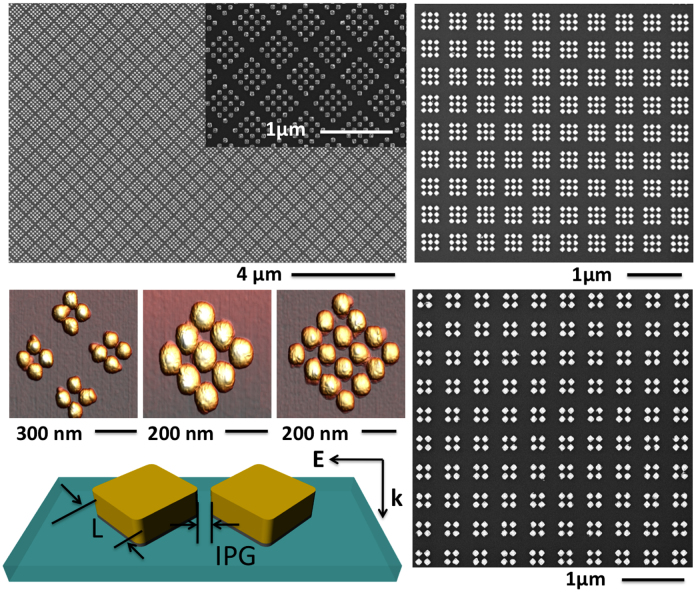
The device, fabricated by means of electron beam lithography (EBL), consists of a series of metallic cuboids (square-like) endowed with different inter-particle distances (Fig. 1). The present nanostructures, characterized by well-defined corners, were chosen to spatially define and control the local electric field distribution, hence to improve the SERS performance with respect to nanosphere based structures11,33,34.
Figure 1. (a) SEM image of gold-based nanocuboid periodic SERS substrates with 2 × 2, 3 × 3 and 4 × 4 array size; (b) 3D-AFM image of 2 × 2, 3 × 3 and 4 × 4 array size SERS substrate; (c) Cartoon representation of gold-based nanocuboid structures is depicted with all the specifications (L = 80 nm, G = 20–500 nm and H = 25 nm).
Both, the electric field polarization with respect to the nanocuboid diagonal axis and the direction of incident light, are also indicated.
In the past, few works were reported the SERS behavior on periodic square–like nanostructures35,36,37 where very high periodicity (400–740 nm with IPG around 100 nm) was considered. Recently, it was introduced a plasmonic nanocube device38 to increase the LSPR sensitivity by means of Fano resonances, thus confirming the importance of this kind of geometry. In the present paper, we show periodic square-like nanostructures with IPG down to 20 nm, thus ensuring the formation of intense electric field hot-spots inside the gap regions.
At first, we concentrated our efforts into the optimization of SERS device nanostructure parameters. In particular, we have maximized the electric field enhancement either by varying the inter–particle gap in the range of 20–500 nm for a 4 × 4 cuboids matrix, or by changing the dimensions of the matrix (i.e. 1 × 1, 2 × 1, 2 × 2, 3 × 3, 4 × 4 and 12 × 12) maintaining IPG fixed at 20 nm. A monolayer of R6G, deposited on the SERS nanostructures by means of chemisorption technique, was employed as a probe molecule during the initial optimization stage (i.e. to finely tune IPG and matrix dimension). Thereafter, metalloprotein (i.e. myoglobin), synthesized W1837R wild type and mutated peptide were deposited over the optimized device (IPG = 20 nm and 4 × 4 cuboids matrix) in order to investigate the substrate ability as an effective biosensor. In addition, theoretical simulations were performed to show the periodic distribution of the electric field consistent with the geometrical configuration of the nanocuboid matrix. As expected, hot-spots were identified in the regions surrounding the cuboid corners.
Results
Nanocuboid SERS substrates with different matrix dimensions were fabricated using top-down EBL technique, followed by gold deposition using e–beam evaporation technique. A flow diagram for SERS device fabrication is shown in Supplementary Fig. S1. In Fig. 1(a), SEM images of nanocuboid SERS substrates with different cuboid matrices (2 × 2, 3 × 3 and 4 × 4) and IPG around 20 nm are demonstrated. A magnified view of the nanocuboids (in order to highlight the morphological quality) is reported in Supplementary Fig. S2. In order to estimate the gold nanostructure height, AFM measurements were performed (see Fig. 1(b)). The height was found to be approximately 25 nm. The image shows no sharp corners of the nanocuboids due to the convolution between the relatively large AFM tip and the nanostructure. A cartoon picture of the nanostructure, illustrating also the laser polarization with respect to the SERS device, is shown in Fig. 1(c).
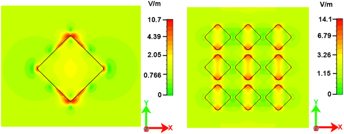
In order to investigate the electric field distribution for this kind of substrate, numerical calculations were performed by finite integration methods (a commercial software: CST microwave studio)39. In particular, the gold nanocuboids were modeled with a geometry as close as possible to the fabricated structures. In fact, as can be observed in Fig. 2, the corners of the cuboids were slightly smoothed to match the experimental geometrical features. The side length of the cuboid structure and IPG were fixed at 80 nm and 20 nm, respectively. The distribution of the electric field, at λ = 633 nm, was calculated for various array sizes from 1 × 1 to 5 × 5 cuboids. In order to avoid any electric field dependence on the mesh density, we have constructed the same mesh density per cuboid for all the array sizes. In Fig. 2, the electric field distributions for the samples with cuboid matrices 1 × 1 and 3 × 3 are shown. The electric field polarization is fixed along the x–axis. It is clearly observed that the electric field is mainly confined on the corners along the y–axis, however, lower electric field can also be revealed on the corners along the x–axis. This behavior is ought to the mismatching resonant conditions between the wavelength and the dimensions of the cuboids. In fact, recently it was reported11 the calculated electric field distribution for an ideal silver nanocuboid under resonant conditions showing a strongly confined field around the corners of the nanocuboid localized along the polarization axis. To be noted that the field enhancement obtained by using a realistic nanocuboid (rounded corners) is expected to be lower than for an ideal structure (sharp corners). Finally, the mesh definition over the nanostructures, together with the comparison between numerical calculations for perfectly sharp and realistic nanocuboids, have been added in the supplementary information (see Supplementary Fig. S3 and S4).
Figure 2. Electric field distribution image for nanocuboids matrix 1 × 1(a) and 3 × 3(b) SERS device.
The corners of the structure are modified to make the design more realistic. The light is x-polarized. Inter particle gap between two nanocuboids is 20 nm.
R6G is an organic fluorescent dye molecule, extensively used in different research fields such as biotechnology, laser gain medium or fluorescence microscopy. SERS measurements were carried out for R6G dye, deposited over different gold–based cuboid SERS substrates using chemisorption technique, in the range of 1080–2000 cm−1. This region was chosen to avoid second-order Si peak. The background Raman spectrum on a bare SERS substrate is shown in the inset of Fig. 3 (see also Supplementary Fig. S4). The featureless Raman spectrum clearly shows the substrate being perfectly clean without any contamination. R6G SERS spectrum is illustrated in Fig. 3, where the characteristics intense peaks are visible at around 1182, 1310, 1361, 1510 and 1649 cm−1, attributed to the out of plane C–Hx bending, the combination of C–H and N–H bending, the combination of ring stretching of C–C vibration, N–H bending and C–Hx wagging, C–H bending, the combination of C–N stretching, C–H and N–H bending, and the combination of ring stretching of C–C vibration and C–Hx bending, respectively40,41,42,43,44. A shoulder at around 1275 cm−1 is also observed, related to the C–O–C stretching vibration of xanthene group. The spectrum was obtained by using a nanocuboid 4 × 4 matrix SERS device with IPG and cuboid side of 20 and 80 nm, respectively.
Figure 3. SERS spectrum, in the range of 1080–2000 cm−1, for R6G dye molecule, deposited on nanocuboids (4 × 4 cuboids matrix size with IPG 20 nm) by means of chemisorption technique.
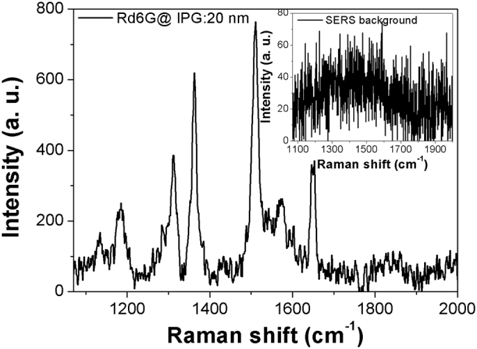
Raman spectrum of bare SERS device (without any molecule on it) is shown in inset.
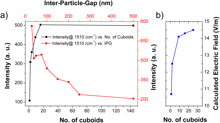
The variation in the reference peak height of R6G SERS spectrum, centered at 1510 cm−1, for all the SERS substrates with IPG in the range of 20–500 nm is plotted in Fig. 4(a) (red line with square symbol ‘ ’). The reference intensity is found to be decreasing with the increase in IPG of the nanocuboid SERS device. The trend in the variation of the intensity can be categorized in two steps: a) the device with IPG less than 250 nm, and b) the device for IPG larger than 250 nm. It is observed that the SERS intensity diminishes quickly (from around 800 counts to 150 counts) when IPG is increased from 20 to 250. Afterwards, SERS intensity remains roughly constant. These intensity variations can be explained using two sharp point interactions. When the IPG is in the range of 20–250 nm, the nanostructures are still sufficiently interacting one another (best interaction condition IPG equals to 20 nm), then the localized plasmons are strongly affected by the coupling between nanocuboids thus intense hot spots are generated. However, when the IPG overcomes 250 nm, it is found that the cuboid nanostructure behaves as an individual structure, causing a decrease in the SERS intensity. In addition, a mapping measurement was performed for a SERS device with IPG around 250 nm, over which the R6G was deposited. The grid area, shown in Supplementary Fig. S5, is the region where the mapping measurement was performed. The markers, fabricated to localize the nanostructures, are clearly visible in the figure. The Raman mapping analysis was centered at 1360 cm−1, the characteristic band of R6G. The step size for the mapping measurement was fixed to 150 nm. Various intense points within the Raman image are clearly visible, corresponding to the best functioning of SERS conditions. Considering that the dimensions of the cuboids (80 nm) results too small to be visible under optical microscope, SERS mapping measurements with fine step size results to be extremely useful to localize and investigate the molecules.
Figure 4. (a) SERS intensity of R6G characteristic band@1510 cm−1 by varying the array size (black line with square symbol ‘ ’) and by varying IPG (red line with square symbol ‘
 ’); (b) plot of calculated electric field (V/m) by varying the cuboids matrix.
Furthermore, a series of SERS measurements were performed for devices with varying cuboids matrix sample and metrology, keeping the IPG fixed (i.e. around 20 nm). Cuboids matrix such as 1 × 1, 2 × 1, 2 × 2, 3 × 3, 4 × 4, and 12 × 12 were investigated to understand their influence on the SERS intensity. In Fig. 4(a) (black line with square ‘ ’), the SERS intensity is plotted vs. the number of cuboids (e.g. in case of 2 × 1, the number of cuboids is 2 while for 4 × 4, it is 16). It is revealed from Fig. 4(a) that the increase in number of cuboids leads to a sharp increase in SERS intensity reaching to 500 counts for the device with 4 × 4 nanostructures. Any further increase in the array size has, however, a little influence on SERS intensity. This trend can be easily understood considering that a 4 × 4 cuboids matrix covers an area of 0.3 μm2 which corresponds to the surface area illuminated by the source light. Hence, an increase in dimension of the nanostructure array will not influence the SERS intensity.
Discussion
In order to verify the experimental results, a comparative study was made between the theoretical electrical field and the experimental SERS intensity as shown in Fig. 4b. It is very clear that the maximum simulated electric field varies sharply from 1 × 1 to 3 × 3 cuboids matrix and, thereafter, increases slowly and seems to be almost saturated for 5 × 5 nanostructures. The trend of varying calculated electric field is found to be consistent with the experimentally observed SERS intensity, the latter determined by choosing the source light matching a surface area of a 4 × 4 cuboids matrix. SERS enhancement factor, on the basis of the results obtained and the parameters used for measurements, is 1.4 × 10⁵ with respect to the gold bar (see inset of Supplementary Fig. S6) placed on the same SERS device. Since, the maximum SERS signal is originated from the corners of the cuboids, only their surface areas were considered for SERS enhancement factor (see Supplementary information: section 5).
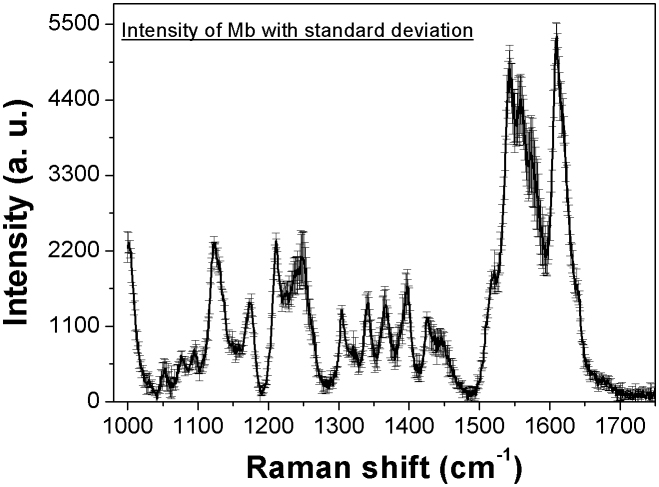
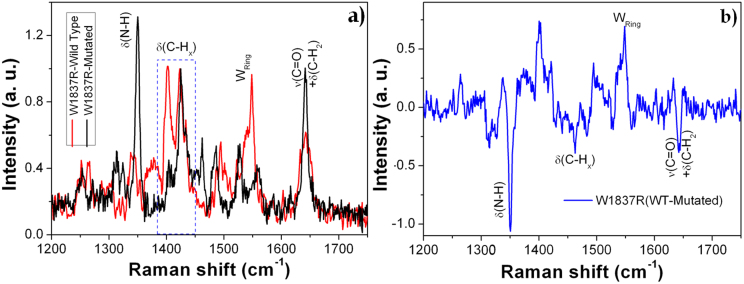
To demonstrate the cuboids matrix capability as biosensor, we have also investigated both myoglobin (Mb) and the labeled-free W1837R peptide of BRCT domain of the BRCA1 tumor protein, deposited over a 4 × 4 cuboids nanostructure. Various measurements were performed for Mb at different locations of the SERS device. Mb SERS spectrum with standard deviation is shown in Fig. 5 (see also Supplementary information: section 6). The standard deviation error bars throughout the spectral range indicate the reproducible behavior of the SERS device and thus the hot-spots generation at different locations. Regarding the W1837R peptide, we have employed the cuboids SERS devices to distinguish its wild form from the mutated one. The peptides structures (wild and mutated types) are shown in Supplementary Fig. S7. These peptides contain 16 amino acids in a sequence in which one amino acid, i.e. tryptophan (W), is substituted by arginine (R), keeping the other amino acids as in the sequence. SERS measurements were performed for both peptides in the range of 1200–1750 cm−1, as shown in Fig. 6(a). The spectra show the various peaks related to C = O stretching, C–Hx bending, C–N stretching vibrations throughout the spectral range. To have a better understanding of the response from the two forms of peptide, their difference SERS spectrum (WT-Mutated) is also plotted in Fig. 6(b). The graph shows the spectral difference between wild type and mutated peptide. In particular, the positive difference values for the band centered at around 1549 and 1402 cm−1 are related to the ring breathing vibration and aromatic CHx bending vibration (wild type)29,34,45 and the negative values for the band centered at 1350 and 1645 cm−1 are attributed to the δN–H and combined vibrational of νC = O and δC–Hx (mutated), respectively. Furthermore, the wild type peptide expresses the aromatic benzene ring related vibration, whereas the mutated peptide shows an excess N–H and aliphatic C–Hx from arginine amino acid.
Figure 5. Myoglobin SERS spectrum, deposited over a nanocuboid structure, in the range of 1000–1750 cm−1 with standard deviation.
The length of standard deviation bar demonstrates little variation of the myoglobin spectra at different locations of the SERS device.
Figure 6. (a) SERS spectra of W1837R (wild type and mutated) peptides of BRCT domain of BRCA1 tumor protein with the associated chemical vibrations; (b) difference SERS spectrum of (WT-Mutated) peptide.
To resume, these measurements, aside a good reproducibility, show that the present simple SERS geometry and architecture is suitable for high sensitivity detection and for revealing point-mutation (single aminoacid substitution) when isolated small peptides are analyzed.
In summary, we have fabricated a reproducible Au-nanocuboid array SERS device by using a top-down nanofabrication technique, following a careful protocol regarding the lift-off and the EBL parameters. This technique offers a great control over the size and IPG of the metallic nanocuboids, hence a strict control over plasmon resonance generation. This procedure was used to fabricate nanocuboids matrix of different dimensions (1 × 1, 2 × 2, 3 × 3, 4 × 4 and 12 × 12) and with various IPG (cuboid corner-to-corner from 20–500 nm). Morphological assessments were carried out by means of SEM and AFM while SERS measurements were employed to verify the device reliability as a biosensor. Numerical simulations were also performed and found them consistent with the experimental SERS results.
After depositing R6G, SERS measurements were performed for all the samples by varying the matrix dimensions (from 1 × 1 to 12 × 12) and by varying the IPG (in the range of 20–500 nm). SERS enhancement is estimated to be 1.4 × 10⁵ with respect to the gold bar. Thereafter, 4 × 4 array devices were chosen to further investigate the Raman signature of Mb protein and W1837R peptides (wild type and mutated). Using this SERS device, over which a monolayer deposition was made, we were able to distinguish wild type W1837R peptide from the mutated one in a label-free manner. The present research opens up a new path for biomedical applications based on SERS devices by improving the early detection capability of several diseases such as cancer, where small variations in the peptide sequence can originate the formation of tumors.
Methods
Design and fabrication of SERS device
Au-cuboid nanostructured arrays were fabricated by electron–beam lithography (EBL) on Si substrates. A 85 nm thick layer of Polymethyl methacrylate (PMMA) resist was spin–coated on top of the cleaned Si surfaces. Thereafter, the resist films were dried in air at 180°C for 8 min. An e–beam direct writing system (Raith150-Two) was used to define the pattern operating at 30 keV with electron dosage of 624 μC/cm2. After developing the resist in a 1:3 solution of Methyl Isobutyl Ketone (MIBK) and Isopropyl alcohol (IPA) for 40 s, Ti and Au were deposited by means of electron–beam evaporation technique (Kurt J Lesker PVD system). Finally, nanostructured arrays were formed after lift–off in acetone for two minutes under ultrasonic bath.
Morphology analysis
The surface morphology of the substrates was characterized by using scanning electron microscope (SEM) and atomic force microscope (AFM). The side length ‘L’ and height ‘H’ of the each square nanostructure was around 80 and 25 nm, respectively. The average inter–particle gap was found down to 20 nm.
SEM measurements (JSM–7500FA, Jeol, Japan) were performed on the cuboid substrates, keeping 15 kV of acceleration voltage for the primary electron beam and collecting the topographic signal from the secondary electrons. SEM images of nanocuboid SERS substrates with different array size (2 × 2, 3 × 3 and 4 × 4) are shown in Fig. 1(a).
AFM measurements were performed on SERS substrates with a Veeco multimode (NanoScope V controller), equipped with ultra-sharp Si probes (ACLA-SS, AppNano; nominal apex diameter: 10 nm) and operating in tapping mode. AFM measurements for all the SERS substrates with different array size were performed. Fig. 1(b) illustrates representative AFM images of SERS substrates with 2 × 2, 3 × 3 and 4 × 4 matrix dimensions. Ought to the convolution of the AFM tip and the sample surface, the sharp corner/edge is not clearly evident. The height of the nanostructure is found to be in the range of 25–30 nm.
Chemical analysis
Raman scattering measurements were performed by Renishaw inVia microscope. Microprobe Raman spectra were excited by 633 nm laser line in backscattering geometry through a 150× objective (NA = 0.95) with the laser power fixed to 0.17 mW and the accumulation time 30 sec. The bare SERS device Raman spectrum is shown in inset of Fig. 2. Different molecules (R6G, myoglobin and W1837R peptides, all from sigma aldrich), deposited over the SERS devices by means of chemisorption technique, were investigated. The concentration of all the molecules is in the μM range. All the SERS spectra were initially baseline–corrected using maximum 3rd order polynomial with the help of WiRE 3.0 software.
Electric field calculation
With the aim of providing additional information on the Raman behavior of SERS devices, numerical simulations of gold based cuboid nanostructures with 25 nm height were performed keeping the incident light wavelength at 633 nm. In order to well represent the experimental situation, the simulated structure was built by using an adaptive tetragonal mesh. This aspect plays a crucial role especially for structures showing small details in an overall extended domain. In particular, the mesh density is kept higher at the edge/corner of the cuboids, as shown in Supplementary Fig. S3. Using this customized tetragonal mesh construction, it is possible to reach calculation with the spatial resolution down to 0.5 nm. In our case, the extension of the three dimensional domain was of 900 nm × 900 nm × 200 nm with a resolution of less than 0.5 nm.
Author Contributions
G.D., A.T. and E.D. envisaged and designed the experiments, M.C. and M.L. fabricated SERS device, A.G., R.P.Z. and A.A. carried out SERS measurements and electric field simulations, respectively. G.D., A.T., R.P.Z. and E.D. analyzed the data and engaged in writing paper. All the authors discussed the results and finalized the manuscript.
Supplementary Material
Supplementary Info
References
- Ye J. et al. Plasmonic Nanoclusters: Near Field Properties of the Fano Resonance Interrogated with SERS. Nano Letters 12, 1660–1667 (2012). [DOI] [PubMed] [Google Scholar]
- Xu H. X., Bjerneld E. J., Kall M. & Borjesson L. Spectroscopy of single hemoglobin molecules by surface enhanced Raman scattering. Physical Review Letters 83, 4357–4360 (1999). [Google Scholar]
- Ahijado-Guzman R., Gomez-Puertas P., Alvarez-Puebla R. A., Rivas G. & Liz-Marzan L. M. Surface-Enhanced Raman Scattering-Based Detection of the Interactions between the Essential Cell Division FtsZ Protein and Bacterial Membrane Elements. Acs Nano 6, 7514–7520 (2012). [DOI] [PubMed] [Google Scholar]
- Anker J. N. et al. Biosensing with plasmonic nanosensors. Nature Materials 7, 442–453 (2008). [DOI] [PubMed] [Google Scholar]
- Nie S. M. & Emery S. R. Probing single molecules and single nanoparticles by surface-enhanced Raman scattering. Science 275, 1102–1106 (1997). [DOI] [PubMed] [Google Scholar]
- Kneipp K., Kneipp H., Itzkan I., Dasari R. R. & Feld M. S. Surface-enhanced Raman scattering and biophysics. Journal of Physics-Condensed Matter 14, R597–R624 (2002). [Google Scholar]
- Li Z.-Y. & Xia Y. Metal Nanoparticles with Gain toward Single-Molecule Detection by Surface-Enhanced Raman Scattering. Nano Letters 10, 243–249 (2010). [DOI] [PubMed] [Google Scholar]
- Fang C. et al. DNA detection using nanostructured SERS substrates with Rhodamine B as Raman label. Bionsensors and bioelectronics 24, 216–221 (2008). [DOI] [PubMed] [Google Scholar]
- Sagmuller B., Schwarze B., Brehm G. & Schneider S. Application of SERS spectroscopy to the identification of (3,4-methylenedioxy) amphetamine in forensic samples utilizing matrix stabilized silver halides. Analyst 126, 2066–2071 (2001). [DOI] [PubMed] [Google Scholar]
- Cabrini S. et al. Focused ion beam lithography for two dimensional array structures for photonic applications. Microelectronic Engineering 78–79, 11–15 (2005). [Google Scholar]
- McLellan J. M., Li Z.-Y., Siekkinen A. R. & Xia Y. The SERS activity of a supported ag nanocube strongly depends on its orientation relative to laser polarization. Nano Letters 7, 1013–1017 (2007). [DOI] [PubMed] [Google Scholar]
- Chen H., Kou X., Yang Z., Ni W. & Wang J. Shape- and size-dependent refractive index sensitivity of gold nanoparticles. Langmuir 24, 5233–5237 (2008). [DOI] [PubMed] [Google Scholar]
- Fazio B. et al. Re-radiation Enhancement in Polarized Surface-Enhanced Resonant Raman Scattering of Randomly Oriented Molecules on Self-Organized Gold Nanowires. Acs Nano 5, 5945–5956 (2011). [DOI] [PubMed] [Google Scholar]
- Graham D., Thompson D. G., Smith W. E. & Faulds K. Control of enhanced Raman scattering using a DNA-based assembly process of dye-coded nanoparticles. Nature Nanotechnology 3, 548–551 (2008). [DOI] [PubMed] [Google Scholar]
- Dieringer J. A., Lettan I. I. R. B., Scheidt K. A. & Van Duyne R. P. A frequency domain existence proof of single-molecule surface-enhanced Raman Spectroscopy. Journal of the American Chemical Society 129, 16249–16256 (2007). [DOI] [PubMed] [Google Scholar]
- Camden J. P. et al. Probing the structure of single-molecule surface-enhanced Raman scattering hot spots. Journal of the American Chemical Society 130, 12616–12617 (2008). [DOI] [PubMed] [Google Scholar]
- Le Ru E. C., Etchegoin P. G. & Meyer M. Enhancement factor distribution around a single surface-enhanced Raman scattering hot spot and its relation to single molecule detection. Journal of Chemical Physics 125, 204701–204701 (2006). [DOI] [PubMed] [Google Scholar]
- Otto A. The ‘chemical’ (electronic) contribution to surface-enhanced Raman scattering. Journal of Raman Spectroscopy 36, 497–509 (2005). [Google Scholar]
- Le Ru E. C., Blackie E., Meyer M. & Etchegoin P. G. Surface enhanced Raman scattering enhancement factors: a comprehensive study. Journal of Physical Chemistry C 111, 13794–13803 (2007). [Google Scholar]
- Mock J. J., Barbic M., Smith D. R., Schultz D. A. & Schultz S. Shape effects in plasmon resonance of individual colloidal silver nanoparticles. Journal of Chemical Physics 116, 6755–6759 (2002). [Google Scholar]
- Dasary S. S. R., Singh A. K., Senapati D., Yu H. & Ray P. C. Gold Nanoparticle Based Label-Free SERS Probe for Ultrasensitive and Selective Detection of Trinitrotoluene. Journal of the American Chemical Society 131, 13806–13812 (2009). [DOI] [PubMed] [Google Scholar]
- Alvarez-Puebla R. A., Zubarev E. R., Kotov N. A. & Liz-Marzan L. M. Self-assembled nanorod supercrystals for ultrasensitive SERS diagnostics. Nano Today 7, 6–9 (2012). [Google Scholar]
- Sans V. et al. SE(R)RS devices fabricated by a laser electrodispersion method. Analyst 136, 3295–3302 (2011). [DOI] [PubMed] [Google Scholar]
- Chung A. J., Huh Y. S. & Erickson D. Large area flexible SERS active substrates using engineered nanostructures. Nanoscale 3, 2903–2908 (2011). [DOI] [PubMed] [Google Scholar]
- Rodriguez-Lorenzo L., de la Rica R., Alvarez-Puebla R. A., Liz-Marzan L. M. & Stevens M. M. Plasmonic nanosensors with inverse sensitivity by means of enzyme-guided crystal growth. Nature Materials 11, 604–607 (2012). [DOI] [PubMed] [Google Scholar]
- Kahl M., Voges E., Kostrewa S., Viets C. & Hill W. Periodically structured metallic substrates for SERS. Sensors and Actuators B-chemical 51, 285–291 (1998). [Google Scholar]
- Yan B. et al. Engineered SERS Substrates With Multiscale Signal Enhancement: Nanoplarticle Cluster Arrays. Acs Nano 3, 1190–1202 (2009). [DOI] [PubMed] [Google Scholar]
- Guillot N. et al. Surface enhanced Raman scattering optimization of gold nanocylinder arrays: Influence of the localized surface plasmon resonance and excitation wavelength. Applied Physics Letters 97, 023113–023113 (2010). [Google Scholar]
- De Angelis F. et al. Nanoscale chemical mapping using three-dimensional adiabatic compression of surface plasmon polaritons. Nature Nanotechnology 5, 67–72 (2010). [DOI] [PubMed] [Google Scholar]
- Chen Y. et al. Electrically Induced Conformational Change of Peptides on Metallic Nanosurfaces. Acs Nano 6, 8847–8856 (2012). [DOI] [PMC free article] [PubMed] [Google Scholar]
- De Angelis F. et al. Breaking the diffusion limit with super-hydrophobic delivery of molecules to plasmonic nanofocusing SERS structures. Nature Photonics 5, 683–688 (2011). [Google Scholar]
- Di Fabrizio E. et al. Fabrication of 5 nm resolution electrodes for molecular devices by means of electron beam lithography. Japanese Journal of Applied Physics, Part 2: Letters 36, L70–L72 (1997). [Google Scholar]
- Rycenga M., Camargo P. H. C., Li W., Moran C. H. & Xia Y. Understanding the SERS Effects of Single Silver Nanoparticles and Their Dimers, One at a Time. Journal of Physical Chemistry Letters 1, 696–703 (2010). [DOI] [PMC free article] [PubMed] [Google Scholar]
- David C., Guillot N., Shen H., Toury T. & de la Chapelle M. L. SERS detection of biomolecules using lithographed nanoparticles towards a reproducible SERS biosensor. Nanotechnology 21, 475501–475501 (2010). [DOI] [PubMed] [Google Scholar]
- Hou Y., Xu J., Zhang X. & Yu D. SERS on periodic arrays of coupled quadrate-holes and squares. Nanotechnology 21, 195203–195203 (2010). [DOI] [PubMed] [Google Scholar]
- Beermann J., Novikov S. M., Leosson K. & Bozhevolnyi S. I. Surface enhanced Raman microscopy with metal nanoparticle arrays. Journal of Optics A-pure and Applied Optics 11, 075004–075004 (2009). [DOI] [PubMed] [Google Scholar]
- Yokota Y., Ueno K. & Misawa H. Highly Controlled Surface-Enhanced Raman Scattering Chips Using Nanoengineered Gold Blocks. Small 7, 252–258 (2011). [DOI] [PubMed] [Google Scholar]
- Zhang S., Bao K., Halas N. J., Xu H. & Nordlander P. Substrate-Induced Fano Resonances of a Plasmonic: Nanocube: A Route to Increased-Sensitivity Localized Surface Plasmon Resonance Sensors Revealed. NANO LETTERS 11, 1657–1663 (2011). [DOI] [PubMed] [Google Scholar]
- Frezza F., Pajewski L. & Schettini G. Full-wave characterization of three-dimensional photonic bandgap structures. IEEE Transactions on Nanotechnology 5, 545–553 (2006). [Google Scholar]
- Coluccio M. L. et al. Silver-based surface enhanced Raman scattering (SERS) substrate fabrication using nanolithography and site selective electroless deposition. Microelectronic Engineering 86, 1085–1088 (2009). [Google Scholar]
- Mondal B. & Saha S. K. Fabrication of SERS substrate using nanoporous anodic alumina template decorated by silver nanoparticles. Chemical Physics Letters 497, 89–93 (2010). [Google Scholar]
- Jensen L. & Schatz G. C. Resonance Raman scattering of rhodamine 6G as calculated using time-dependent density functional theory. Journal of Physical Chemistry A 110, 5973–5977 (2006). [DOI] [PubMed] [Google Scholar]
- Yajima T., Yu Y. & Futamata M. Closely adjacent gold nanoparticles linked by chemisorption of neutral rhodamine 123 molecules providing enormous SERS intensity. Physical Chemistry Chemical Physics 13, 12454–12462 (2011). [DOI] [PubMed] [Google Scholar]
- Vosgr√∂ne T. & Meixner A. J. Surface- and resonance-enhanced micro-raman spectroscopy of xanthene dyes: From the ensemble to single molecules. ChemPhysChem 6, 154–163 (2005). [DOI] [PubMed] [Google Scholar]
- Das G. et al. Nano-patterned SERS substrate: Application for protein analysis vs. temperature. Bionsensors and bioelectronics 24, 1693–1699 (2009). [DOI] [PubMed] [Google Scholar]
Associated Data
This section collects any data citations, data availability statements, or supplementary materials included in this article.
Supplementary Materials
Supplementary Info


