Abstract
We present a new noise shaping method and a dual polarity calibration technique suited for successive approximation register type analog to digital converters (SAR-ADC). Noise is pushed to higher frequencies with the noise shaping by adding a switched capacitor. The SAR capacitor array mismatch has been compensated by the dual-polarity digital calibration with minimum circuit overhead. A proof-of-concept prototype SAR-ADC using the proposed techniques has been fabricated in a 0.5-μm standard CMOS technology. It achieves 67.7 dB SNDR at 62.5 kHz sampling frequency, while consuming 38.3μW power with 1.8 V supply.
Keywords: Analog-to-digital converter, SAR ADC, digital calibration, noise shaping
I. Introduction
Analog-to-digital converters (ADC) using the charge redistribution property of the successive-approximation-register (SAR) show considerable power efficiency, and so they are being widely used in low power and low frequency applications, such as medical devices. As a result of the in-depth research on the SAR architecture and due to prevalence of the CMOS process, the SAR-ADC is aggressively extending into both high frequency domain of several tens of MHz and high resolution in the order of 14-16 bits [1], [1]. However, such performance improvements often come at the cost of increased design complexity or the power/area consumption. Many designers of low power applications, who adopt the SAR-ADC architecture, are still looking for solutions that would increase the ADC resolution without sacrificing its simplicity and the power/area efficiency. In this paper, we present a new noise shaping method, which can be easily added to an existing SAR-ADC structure, along with a dual-polarity digital calibration method, which compensates the capacitor mismatch with minimal circuit burden.
If the error between the analog input and the digitized output can be delivered to the next conversion cycle, the quantization noise is high-pass filtered and pushed into higher frequencies [2]. Researchers have found several ways to incorporate the noise shaping effect in the VCO-based, dual-slope, and flash ADCs. These are either implemented as stand-alone ADCs or used as a single-bit or a multi-bit quantizer for Δ∑ ADCs depending on the application requirements [3]-[7]. The SAR-ADC architecture also has the potential for applying the noise shaping technique considering the fact that the internal charge redistribution digital-to-analog converter (crDAC) capacitors keep a residual charge at the end of the conversion period. If this residual charge can be delivered to the next conversion cycle, the signal-to-noise ratio (SNR) will be increased via noise shaping without significant modifications in the basic SAR architecture [8], [9]. The additional circuit for noise shaping, however, should be carefully designed not to degrade the built-in crDAC performance, which is key in determining the ADC resolution. The proposed noise shaping method delivers the residual charge by adding a single switched capacitor in parallel to the top plate of the crDAC, in a way that it will not degrade the original ADC performance.
For the SAR-ADCs with moderate resolution in the order of 10 effective number of bits (ENOB), resolution is often limited by the capacitor mismatch, as opposed to the small DAC voltage steps, which is the main reason that limits the resolution in high resolution ADCs with low supply voltage [1], [8]. Furthermore, capacitor mismatch is more serious in the low cost processes without high precision multilayer metal-insulator-metal (MIM) capacitors, which should rely on poly-poly capacitors with large bottom plate parasitic capacitance of 10-20% [10]. Therefore, calibration is necessary to minimize capacitor mismatch and the resulting performance degradation.
Calibration can be done either in the analog domain by adding an auxiliary DAC or in the digital domain after the digitized code is generated [11], [12]. Digital calibration has the advantage of low complexity if it is completed in the foreground before the normal ADC operation starts. If the calibration is executed continuously in the background, transparent to the normal ADC operation, it can be more accurate and be responsive to varying environmental conditions, such as temperature. There is, however, a level of circuit overhead in addition to digital code redundancy [1], [12]. We have adopted foreground digital calibration to minimize the burden of calibration circuitry. Moreover, previous calibration methods require a comparator calibration to cut the comparator offset before the capacitor calibration, which is yet another overhead [13], [13]. The proposed dual-polarity digital calibration conducts the comparator calibration along with the capacitor calibration by repeating the calibration of each binary capacitor with two polarities.
II. Noise Shaping
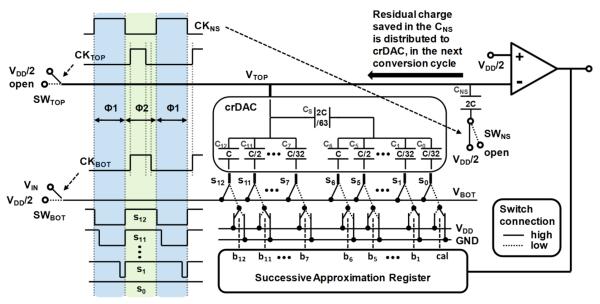
Fig. 1 depicts the overall architecture of the proposed SAR-ADC with the noise shaping. A 12-bit crDAC is implemented as a pair of 6-bit capacitive arrays connected by a splitting capacitor. The split-array topology was adopted to reduce area and dynamic power consumption. A static latched comparator was selected to minimize the kickback noise [14]. By controlling two switches connected each at top and bottom plate of the crDAC (SWTOP and SWBOT) with the right sequence described in Fig. 1, the input voltage is sampled at the total capacitance of the crDAC (CDAC) with the stored charge of,
| (1) |
Fig. 1.
Overall architecture of the proposed SAR-ADC with timing diagram of its sampling clocks.
Subsequently, a 13-bit serial digital output stream is generated from the comparator output by deciding the status of 12 switches at the bottom plate of each binary scaled capacitor to either supply (VDD) or ground (GND) from VDD/2 according to the previous comparator output. At the end of the DAC conversion period, a residual charge will remain and present a residual voltage (ΔVRES) at the top plate of the crDAC, which is smaller than the minimum DAC output voltage resolution. By adding a capacitor (CNS) with a switch (SWNS) for noise shaping, the residual charge can be saved and delivered to the next conversion cycle.
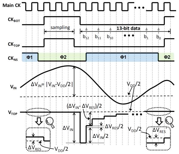
Detailed operating diagram of the noise shaping function is shown in Fig. 2. During the phase Φ1, the SWNS is connected to VDD/2 and the DAC conversion takes place for twelve times till the voltage at the top plate of the crDAC (VTOP) shows VDD/2±ΔVRES. At the end of phase Φ1, CNS is charged with a residual charge QRES,
| (2) |
and the SWNS is opened before the top plate of the crDAC is connected to VDD/2. Thus, the CNS maintains its stored charge of QRES. During phase Φ2, the input voltage, VIN, is sampled while keeping SWNS open to conserve the QRES in CNS. SWNS is closed at the beginning of the next Φ1 phase after both the SWTOP and the SWBOT are toggled to low. The residual error charge, QRES in CNS, is then merged with the sampled input charge, QIN in CDAC, as the two capacitors are connected in parallel, and their voltages are averaged (since CNS = CDAC) at the onset of Φ1. As a result, a noise shaping property is achieved.
Fig. 2.
Operating diagram of the SAR-ADC with noise shaping.
The proposed noise shaping method of the SAR-ADC is based on the charge sharing between CDAC and CNS. When SWNS is connected to VDD/2, the charge captured in CDAC by the input sampling (QIN) is shared with the residual charge in CNS (QRES). Thus, VTOP is determined according to both the input voltage level and the residual charge from previous conversion cycle. Using the law of conservation of charge, VTOP at the beginning of the next conversion cycle, VTOP’, can be calculated from,
| (3) |
Since CNS is designed to have the same size as CDAC, (3) can be simplified to,
| (4) |
Therefore, the sampled input (VDD/2-VIN) and the residual error (VTOP-VDD/2) are averaged. Accordingly, the relationship between the sampled analog input X[n], the digital output D[n], and the quantization error qe[n] can be described as,
| (5) |
The maximum attenuation of the quantization noise that can be achieved is by half, which implies that a maximum improvement of signal to noise ratio (SNR) would be 6 dB from noise shaping. However, the maximum noise attenuation can be increased with the ratio of CNS to the CDAC. The ratio between these two capacitors determines the coefficient of the residual error that is delivered to the next conversion cycle. If CNS = k × CDAC, then from (3) we can find,
| (6) |
where k determines the coefficient of the noise shaping component. For example, if k is increased to 3, (5) can be changed to
| (7) |
and the maximum noise attenuation is ¼ along with maximum SNR improvement of 12 dB.
The size of the CNS also changes the crDAC step size (ΔVLSB) based on (6), that is, variations in VTOP tend to decrease as the weight of noise shaping increases. However, it is not a serious concern in ADCs with moderate resolution considering that the input referred noise of the comparator, Vn-CMP, is much smaller than the minimum voltage resolution of the crDAC, ΔVLSB. For instance, in the presented 13-bit ADC with k=1, Vn-CMP ≈ 0.1 × ΔVLSB. Nevertheless, the trade-off between the weight of noise shaping and ΔVLSB should be considered in the design stage. It should be also noted that CNS neither needs a high level of accuracy as the crDAC capacitors nor a special care for matching in its layout. This will give designers the flexibility to layout CNS within the remaining dead space on the chip.
III. Dual-Polarity Digital Calibration
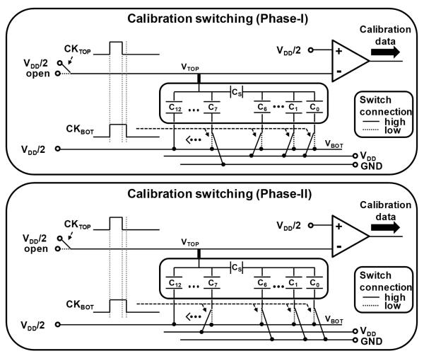
In SAR-ADCs with binary-weighted crDACs, the size of the nth bit capacitor, C/212-n in Fig. 1, is the same as the sum of all smaller capacitors combined. For instance in Fig. 3, C7 is ideally equal to the series combination of CS and ∑Ci (i = 0 to 6). Therefore, if we charge Cn up to a certain voltage, e.g. VDD/2, and also charge the smaller capacitors up to the same voltage but with the opposite polarity, i.e. -VDD/2, when we connect all of them in parallel, the charges should ideally cancel out and the mismatch voltage should be zero. On the other hand, if there was a mismatch between C7 and the smaller capacitors, the amount of the mismatch voltage after charge cancellation would be an indicator of the amount of capacitor mismatch, and one can digitize that voltage to calibrate the 7th bit [11].
Fig. 3.
Switching sequence for the dual-polarity digital calibration.
We applied this calibration method only to the MSB half of the split array (C7 to C12 in Fig. 3) due to its significance in the SAR-ADC operation, and considered the LSB half to be accurate. The mismatch of the LSB half is negligible because its numerical value (binary weight) is 2−6 times of its physical size when using the split array architecture. During calibration process, initially all capacitors were discharged by connecting their top and bottom plates to VDD/2. Then in Phase-I calibration, shown in Fig. 3, the bottom plate of C7 was connected to GND, charging it to VDD/2, and the bottom plates of C0 to C6 were connected to VDD, charging the series combination of CS and C0:6 to -VDD/2. At the falling edge of CKTOP, the top plate detaches from VDD/2 and at the falling edge of CKBOT, all bottom plates switch back to VDD/2, thus connecting all capacitors in parallel. VTOP at this time represents the mismatch in C7, and the SAR-ADC digitization function, running only on the LSB half, provides the amount of calibration needed to compensate for this mismatch. The same process is then applied to C8 to C12. It should be noted that any possible mismatch in the splitting capacitor, CS, will already be considered after completing the calibration process for each capacitor in the MSB half of the array [13].
Another source of error in the SAR-ADCs is the comparator offset. Because VTOP after the calibration process is very close to VDD/2, even a slight offset in the comparator input can affect the calibration results [13]. To address this problem, we have adopted a dual-polarity digital calibration mechanism, which repeats the calibration process that was explained earlier, with two opposite polarities, as shown in Fig. 3. In Phase-I, Cn acquires a positive charge (VDD/2) and the smaller capacitors acquire a negative charge (−VDD/2). In Phase-II, however, Cn acquires a negative charge (−VDD/2) and the smaller capacitors acquire a positive charge (VDD/2).
Since the comparator offset affects the digitized value of the mismatch voltage by the same amount and in the same direction in each phase, as a common-mode signal, it can be taken care of by subtracting the resulting calibration value in Phase-I from that of Phase-II, and dividing the result by half. The mismatch voltage caused by the capacitor mismatch acquires a different polarity in each calibration phase, like a differential-mode signal, and doubles after subtracting the results. At the end of this dual-polarity calibration process, we will have an averaged calibration value for each MSB capacitor, C7 to C12.
IV. Measurement Results
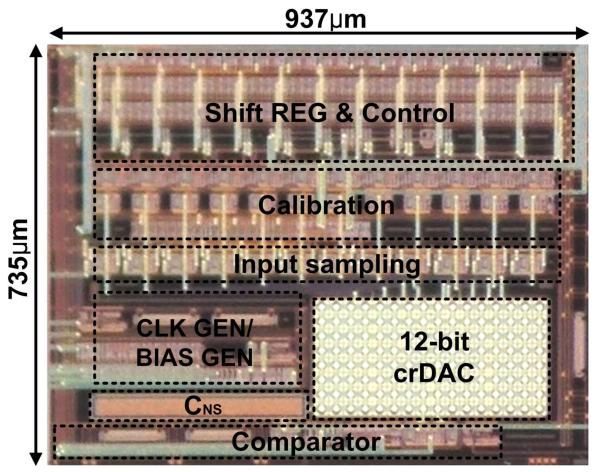
A prototype SAR-ADC was fabricated in the ON-Semi 0.5-μm 3M2P standard CMOS process with poly-insulator-poly (PIP) capacitors. A chip micrograph is shown in Fig. 4 with the active area of 0.689 mm2. It can be seen that CNS, which is added for the noise shaping, occupies a much smaller area compared to the matched crDAC capacitor array, and it has been located within a dead space on the ADC floor plan. The proposed calibration circuitry consumes 13.6% of the entire active area. All measurements were conducted with 1.8V supply and the total SAR-ADC power consumption was 38.3μW at 62.5 kHz sampling rate.
Fig. 4.
Chip micrograph.
Table 1 shows the calibration results of the SAR-ADC, reported in LSB units. Columns two and three show the raw 6-bit digitized outcomes of the mismatch voltage plus comparator offset in Phase-I and Phase-II of the dual-polarity digital calibration process, respectively. In the 4th column, we have subtract Phase-II from Phase-I and divided it by 2 to cancel out the common-mode comparator offset. However, in order to achieve the net mismatch voltage caused by each capacitor mismatch, which also represents the necessary calibration for each bit in LSB, we should consider the fact that while calibrating C8 and above, the mismatch of all the lower capacitors will be included in the raw data. Therefore, to find the specific mismatch of each MSB capacitor of the SAR-ADC in column 5, we need to add all the previous values in column 5 to the value in column 4. Finally, the comparator offset can be found by averaging the result of Phase-I and Phase-II, to find the common-mode value, as shown in the 6th column, with good consistency. These calibration results were delivered to an off-chip microcontroller to compensate the ADC output in the digital domain.
TABLE 1.
SAR-ADC Calibration Results.
| Capacitor Under Calibration |
Phase-I Cal. Output |
Phase-II Cal. Output |
(I−II)/2 | Capacitor Mismatch |
Comp. Offset (I+II)/2 |
|---|---|---|---|---|---|
| C7 | −5 | −5 | 0 | 0 | −5.0 |
| C8 | −5 | −4 | −0.5 | −0.5 | −4.5 |
| C9 | −4 | −5 | +0.5 | 0 | −4.5 |
| C10 | −4 | −5 | +0.5 | 0 | −4.5 |
| C11 | −2 | −8 | +3.0 | +2.5 | −5.0 |
| C12 | −13 | +4 | −8.5 | −6.5 | −4.5 |
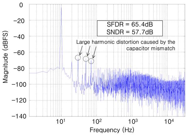
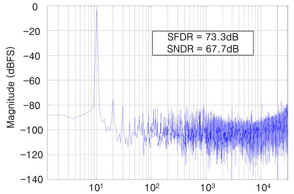
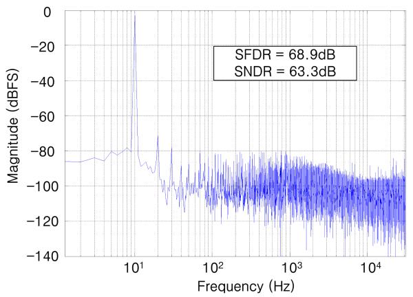
Figs. 5-7 show the spectrum of the SAR-ADC digitized output when a full-scale 1.8 Vp-p sinusoidal input at FIN = 10 Hz was sampled at FS = 62.5 kHz, with and without the noise shaping and dual-polarity digital calibration. The 10 Hz input frequency was selected to observe the effects of noise shaping without them being obscured by the harmonic distortion. To calculate the signal-to-noise plus distortion ratio (SNDR), over sampling ratio of 10 was applied to exclude the high frequency noise, resulting in 3.125 kHz signal bandwidth (BWsignal) [7], [8].
Fig. 5.
FFT of a digitized 10 Hz, 1.8 Vp-p sinusoid without noise shaping, before applying the dual-polarity digital calibration.
Fig. 7.
FFT of the same input as in Fig. 5 after applying both noise shaping and dual-polarity digital calibration.
Before calibration and without noise shaping, Fig. 5 shows several large peaks of harmonic distortion, which are caused by capacitive mismatch. The measured spurious free dynamic range (SFDR) and SNDR in this case were 65.4 dB and 57.7 dB, respectively. After compensating for the crDAC capacitor mismatch via calibration, however, the harmonic distortion components were significantly attenuated, as shown in Fig. 6, and consequently the SFDR and SNDR were improved to 68.9 dB and 63.3dB, respectively. Finally, Fig. 7 shows how the noise floor is pushed upward towards the higher frequencies when we activated the noise shaping mechanism in addition to calibration, which in turn decreases the in-band noise and improves the SFDR and SNDR further to 73.3 dB and 67.7 dB, respectively.
Fig. 6.
FFT of the same input as in Fig. 5 after applying dual-polarity digital calibration, but without noise shaping.
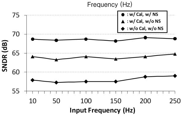
Table 2 summarizes the performance of the SAR-ADC at fixed FS and FIN. Total harmonic distortion (THD) was improved by 8.0 dB with calibration, which implies that the distortion caused by the capacitor mismatch was compensated. The SNR was improved by 6.7 dB by activating the proposed noise shaping mechanism. This result means that the noise floor is reduced almost by half and it matches with the theoretical improvement described in section II. The effect of the noise shaping will become even more remarkable when the THD is increased with linearity improvement, considering that the THD is worse than the SNR in the presented ADC. It should be noted that the foreground calibration adopted in this ADC cannot perfectly compensate the capacitance mismatch. It generates some discontinuity, because it has no redundancy in the digital code [1], [12]. The overall improvements in the SAR-ADC performance can be demonstrated by deriving its ENOB from the SNDR, which was improved from 9.3 to 10.2 bits, and eventually to 11.0 bits with calibration and noise shaping, respectively. Fig 8 shows how the measured SNDR of the SAR-ADC varies with the sinusoidal input frequency.
TABLE 2.
SAR-ADC Performance Summary.
| Test condition | SFDR (dB) |
THD (dB) |
SNR (dB) |
SNDR (dB) |
ENOB (bits) |
|---|---|---|---|---|---|
| w/o Cal*, w/o NS** | 65.4 | 60.6 | 68.6 | 57.7 | 9.3 |
| w/ Cal, w/o NS | 68.9 | 68.6 | 70.1 | 63.3 | 10.2 |
| w/ Cal, w/ NS | 73.3 | 71.4 | 76.8 | 67.7 | 11.0 |
Input signal characteristics: FS = 62.5 kHz, BWsignal = 3.125 kHz, Fin = 10 Hz
Cal: dual-polarity digital calibration,
NS: noise shaping
Fig. 8.
SNDR variations vs. sinusoidal input frequency with and without calibration and noise shaping (FS = 62.5 kHz, BWsignal = 3.125 kHz).
V. Conclusions
A new method for noise shaping has been presented to improve the resolution of the SAR-ADCs with moderate resolution. By simple addition of a switched capacitor to the traditional SAR-ADC architecture, it is possible to deliver the digitization error from one conversion cycle to the next and reduce the in-band noise as a result. We have also demonstrated a dual-polarity digital calibration mechanism to compensate for the capacitor mismatch in the crDAC binary-weighted array with minimum circuit overhead. The presented techniques are easily applicable to a variety of existing SAR-ADCs architectures to improve their performance without adding considerable design burden.
Biography
Hangue Park was born in 1980. He received both B.S. and M.S. degree from Seoul National University, Seoul, Korea, at 2006 and 2008, respectively. From 2001 to 2004, he was with Bluebird-soft, where he designed circuit and system for industrial personal digital assistance (PDA). From 2008 to 2010, he worked for the Samsung-Electronics and designed High-Q RF bandpass filter for SAW-less receiver and PLL for cell-phone applications. He joined GT-Bionics Lab at Georgia Institute of Technology in 2010, where he is currently pursuing his Ph.D. degree. His research interests lies in System and IC design for bio-medical applications, especially in Tongue Drive System.

Maysam Ghovanloo was born in 1973 in Tehran, Iran. He received the B.S. degree in electrical engineering from the University of Tehran, Tehran, Iran, in 1994, the M.S. degree in biomedical engineering from the Amirkabir University of Technology, Tehran, Iran, in 1997, and the M.S. and Ph.D. degrees in electrical engineering from the University of Michigan, Ann Arbor, in 2003 and 2004, respectively.
From 2004 to 2007, he was an Assistant Professor in the Department of Electrical and Computer Engineering, North Carolina (NC) State University, Raleigh. In June 2007, he joined the faculty of Georgia Institute of Technology, Atlanta, where he is currently an Associate Professor and the Founding Director of the GT-Bionics Laboratory in the School of Electrical and Computer Engineering. He has authored or coauthored more than 100 peer-reviewed conference and journal publications.
Dr. Ghovanloo is an Associate Editor of the IEEE TRANSACTIONS ON BIOMEDICAL ENGINEERING, IEEE TRANSACTIONS ON BIOMEDICAL CIRCUITS AND SYSTEMS, and a member of the Imagers, MEMS, Medical, and Displays (IMMD) subcommittee at the International Solid-State Circuits Conference (ISSCC). He is the 2010 recipient of a CAREER award from the National Science Foundation. He has also received awards in the 40th and 41st Design Automation Conference (DAC)/ISSCC Student Design Contest in 2003 and 2004, respectively. He has organized several special sessions and was a member of Technical Review Committees for major conferences in the areas of circuits, systems, sensors, and biomedical engineering. He is a member of the Tau Beta Pi, AAAS, Sigma Xi, and the IEEE Solid-State Circuits Society, IEEE Circuits and Systems Society, and IEEE Engineering in Medicine and Biology Society.
REFERENCES
- [1].Liu W, Huang P, Chiu Y. A 12-bit, 45MS/s, 3-mW redundant successive-approximation-register analog-to-digital converter with digital calibration. IEEE J. Solid-State Circuits. 2011 Nov.vol. 46(no. 11):2661–2672. [Google Scholar]
- [2].McNeill J, Coln MCW, Larivee BJ. Split ADC architecture for deterministic digital background calibration of a 16-bit 1-MS/s ADC. IEEE J. Solid-State Circuits. 2005 Dec.vol. 40(no. 12):2437–2445. [Google Scholar]
- [3].Baker RJ. CMOS: circuit design, layout, and simulation. 2nd ed Wiley-IEEE Press; New Jersey: 2008. pp. 1010–1012. [Google Scholar]
- [4].Yoon Y, Kim J, Jang T, Cho S. A time-based bandpass ADC using time-interleaved voltage-controlled oscillators. IEEE Trans. Circuits Syst. I. 2008 Dec.vol. 55(no. 11):3571–3581. [Google Scholar]
- [5].Pesenti S, Clement P, Kayal M. Reducing the number of comparators in multibit Δ∑ modulators. IEEE Trans. Circuits Syst. I. 2008 May;vol. 55(no. 4):1011–1022. [Google Scholar]
- [6].Naiknaware R, Tang H, Fiez TS. Time-referenced single-path multi-bit Δ∑ ADC using a VCO-based quantizer. IEEE Trans. Circuits Syst. II. 2000 Jul;vol. 47(no. 7):596–602. [Google Scholar]
- [7].Maghari N, Moon U. A third-order DT Δ∑ modulator using noise-shaped bidirectional single-slope quantizer. IEEE J. Solid-State Circuits. 2011 Dec.vol. 46(no. 12):2882–2891. [Google Scholar]
- [8].Fredenburg J, Flynn M. A 90 M/s 11 MHz bandwidth 62 dB SNDR noise-shaping SAR ADC. Proc. IEEE Int. Solid-State Circuits Conf. Dig. Tech. Papers. 2012 Feb.:468–469. [Google Scholar]
- [9].Kim KS, Kim J, Cho SH. nth-order multi-bit ∑Δ ADC using SAR quantiser. Electronics Letters. 2010 Sep.Vol. 46(No. 19) [Google Scholar]
- [10].Razavi B. Design of analog CMOS integrated circuits. 1st ed McGraw-Hill; New York: 2000. pp. 619–624. [Google Scholar]
- [11].Lee H-S, Hodges DA, Gray PR. A self-calibrating 15 bit CMOS A/D converter. IEEE J. Solid-State Circuits. 1984 Dec.vol. SSC-19(no. 6):813–819. [Google Scholar]
- [12].Li J, Moon U. Background calibration techniques for multistage pipelined ADCs with digital redundancy. IEEE Trans. Circuits Syst. II. 2003 Sep.vol. 50(no. 9):531–538. [Google Scholar]
- [13].Yoshioka M, Ishikawa K, Takayama T, Tsukamoto S. A 10-b 50-MS/s 820-μW SAR ADC with on-chip digital calibration. IEEE Trans. Biomedical Circuits Syst. 2010 Dec.vol. 4(no. 6):410–416. doi: 10.1109/TBCAS.2010.2081362. [DOI] [PubMed] [Google Scholar]
- [14].Chen Y, Zhu X, Tamura H, Kibune M, Tomita Y, Hamada T, Yoshioka M, Ishikawa K, Takayama T, Ogawa J, Tsukamoto S, Kuroda T. Split capacitor DAC mismatch calibration in successive approximation ADC. IEEE Custom Integrated Circuits Conf. 2009 Sep.:279–282. [Google Scholar]
- [15].Figueiredo PM, Vital JC. Kickback noise reduction technique for CMOS latched comparators. IEEE Trans. Circuits Syst. II. 2006 Jul;vol. 53(no. 7):541–545. [Google Scholar]


