

Abstract
Determination of the total structure of molecular nanocrystals is an outstanding experimental challenge that has been met, in only a few cases, by single-crystal X-ray diffraction. Described here is an alternative approach that is of most general applicability and does not require the fabrication of a single crystal. The method is based on rapid, time-resolved nanobeam electron diffraction (NBD) combined with high-angle annular dark field scanning/transmission electron microscopy (HAADF-STEM) images in a probe corrected STEM microscope, operated at reduced voltages. The results are compared with theoretical simulations of images and diffraction patterns obtained from atomistic structural models derived through first-principles density functional theory (DFT) calculations. The method is demonstrated by application to determination of the structure of the Au144(SCH2CH2Ph)60 cluster.
Keywords: aberration-corrected microscopy, metal nanoparticles, low voltages, first-principles density functional theory, structure determination
The problem of adequately determining atomic structure at the nanoscale is one that eludes a broadly applicable solution and thereby undermines the confidence of researchers investigating nanostructured materials and nanotechnology generally.1 An exception is the total determination of molecular structure by single-crystal X-ray diffraction, but this method has been applicable in only a few cases, including Pd145 and Au102 metallic cluster compounds, that are mainly in the sub-3-nm range.2,3 This is because it requires a homogenous, macroscopic (≫ 1 μm), single crystal of oriented molecules. Preparation of samples with such a high degree of ordering is unattainable for the vast majority of interesting nanocrystal materials. Electron diffraction (employing state-of-the-art electron microscopy instruments) has the sensitivity for total determination of a single nanostructure, but succeeds mainly on a larger scale (≫ 3 nm) and for non-molecular nanocrystals. The reasons for this are varied, including: intrinsic or induced mobility; damage during long exposure times, the requirement to sample many non-equivalent orientations, and the need to measure a statistically significant number of equivalent structures. These factors combine to bring an uneasy uncertainty regarding the eventual wide use of the electron-microscopy-based electron-diffraction technique to nanocrystals in the small nanoscale range (e.g., particles with ≤ 3nm diameter).
Here we describe and implement a rapid electron-diffraction method that surmounts most of these obstacles. We demonstrate the practicality of this method by determining the atomic structure of the chiral-icosahedral (Au)144(thiolate)60 structure, which has been among the most widely discussed unsolved puzzles of recent years. In this way, nanotechnology4 has moved from the initial era of uncontrolled synthesis to a more stringent control of the shape, size and crystal structure of materials in the nano-scale size range. There is now a wide consensus among the research community that no useful application of these materials at an industrial level can be achieved without fully controlling the synthesis of these compounds.5,6
In the case of metallic nanoparticles, the use of thiolate groups (e.g. 2-phenylethanethiolate) has achieved a more delicate control of the number of metal atoms and ligands.7–10 However, the determination of the atomic structure of the metal cores has proven to be most challenging. It is generally accepted that the best and most reliable approach is X-ray crystallography. Unfortunately, to grow high-quality single crystals of (Au)n(SR)m clusters is, in general, very difficult, albeit breakthroughs have been made recently in the cases such as Au102(SR)44, Au25(SR)18 and Au36(SR)24 clusters.3,11–14 Overall, single crystal growth is still among the outstanding challenges of gold thiolate cluster research.
The alternative approach introduced and demonstrated in this paper, does not require the fabrication of a single crystal and consequently it promises to be of broad applicability. Our method is based on the combination of low-voltage scanning/transmission electron microscopy (STEM) electron diffraction and high-angle annular dark field scanning/transmission electron microscopy (HAADF-STEM) images in a probe corrected STEM microscope. This is combined with theoretical calculations of images and diffraction patterns and density functional theory (DFT) calculations of the particle structure. We have applied the method to the structure determination of a thiolate-protected gold cluster compound, namely Au144(SCH2CH2Ph)60, hereafter denoted by the symbol 1.
The synthesis and purification of 1 have been accomplished by literature procedures, as described in the Supplementary Information (SI).5,15 The samples were characterized by mass spectrometry (MALDI-MS) and by optical absorption spectroscopy (UV-vis-NIR), as well as by high-resolution transmission electron microscopy, with results that are in substantial agreement with those published previously for the pure compound, see Figures S1 and S2 in SI. The TEM/STEM sample grid was prepared by placing 3–4 drops of dilute solution on a holy carbon film coated Cu grid (3 mm, 300 mesh) and dried under room temperature. The HAADF STEM images, nano beam diffraction (NBD) patterns were recorded in a probe Cs-corrected JEOL JEM-ARM 200F operated at 80 kV. HAADF-STM images were obtained with a convergence angle of 26 mrad and the collection semi-angles from 50 to 180 mrad. The probe size used was about 0.09 nm with a probe current of 22 pA. In addition, bright field (BF) STEM images were recorded by using a collection semi-angle of 11 mrad.
The present understanding of the structure of compound 1 and analogous Au144(SR)60 compounds has been altered by recent NMR experiments16 indicating that all 60 thiolates are in symmetry equivalent configurations, which implies a higher effective symmetry than is present in earlier models.17 Accepting this symmetry-equivalence, established for the Au144(pMBA)60 clusters, the question arises, what kind of structure can be consistent with this 60-fold equivalent symmetry? It is incompatible with the reflection symmetry of the full icosahedral group (Ih, of order 120), because each thiolate group is a low-symmetry object. Rather, only the rotational symmetries, about the axes {15 × C2, 10 × C3, 6 × C5}, can be preserved, as in the icosahedral rotation group, or chiral-icosahedral group* (designated I, of order 60). Each of the 60 thiolates is located off these rotation-axes, such that an operation swings the thiolate (SR)-configuration into another ligand’s position. This is best conveyed by considering an actual I-symmetry compliant structure (e.g. the optimized structure model described immediately below and displayed in Figs. 1–3), or the appropriate ideal polyhedron; for a clear exposition of the classification, characteristics and symmetries of polyhedra see reference 18
Figure 1.
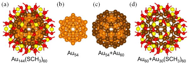
(a) The first-principles-optimized structure of Au144(SR)60 (computationally relaxed with R=CH3), viewed along a 3-fold symmetry axis. (b) The 54-gold atom inner-core is depicted by orange spheres, shown in isolation (labeled Au54). (c) The inner-core together with the surrounding 60-gold atom shell (depicted by brown spheres) form the 114 atom so-called, ‘grand core’, shown by the structure labeled Au54 + Au60. Note the triangular, rhombic, and pentagonal facets characteristic of a 60 atom rhombicosi-dodecahedron. (d) The protective shell is made of 30 RS-Au-SR units, with the S atoms depicted as small red spheres (each ‘carrying a stick’ representing the bond direction to the thiolate tail, R) and the Au atoms are represented by yellow spheres. This protective shell, shown in the image on the right, covers the surface of the 60-Au atom outer shell (brown spheres) with each RS-Au-RS unit anchored (stapled) through the coordination of the sulfur atoms to two gold atoms of the outer-shell.
Figure 3.

(a) Calculated interatomic distances, and (b) radial atomic shell distances from the center of the theoretically optimized Au144(SH)60 cluster. The different atomic shells are labeled as follows: AuC1 – the 12-gold atom innermost shell; AuC2 – the next 42 gold atom shell (AuC1+ AuC2 constitute the 54-gold atom inner core, see Fig. 1). The AuC2 shell may be divided further into the inner 30-Au atom subshell, AuC2(30), and the outer 12-Au atom subshell AuC2(12); AuC3 – the 60- gold atom shell surrounding the inner core (see brown colored atoms in Fig. 1); Auad – the 30 gold atoms in the RS-Au-SR stapling units, and S1 – the 60 sulfur atoms in the stapling units. The interatomic distances in the upper panel (a) are distinguished as follows: (a): Auad-S1 (60 bonds), (b): AuC3-S1 (60 bonds), (c1): AuC2-AuC3 (shorter 60 bonds), (c2): AuC2-AuC3 (longer 120 bonds), (d): AuC1-AuC1 (30 bonds), (e): AuC1-AuC2 (12+30×2=72 bonds), (f):AuC3-AuC3 (triangles) (60 bonds), (g): AuC2-AuC2 (120 bonds), (h1): AuC3-AuC3 (shorter 60 bonds), (h2): AuC3-AuC3 (longer 60 bonds), (i): AuC3-AuC3 (pentagons) (60 bonds). In each category, bonds are sorted and numbered (bond index). For each bond index (vertical axis), a circle is drawn at its corresponding bond length value (horizontal axis). In the calculations of the interatomic distributions in (a), we consider only shorter-range distances; that is, distances in the range of nearest-neighbor, and sometime (for example c1, c2, and h1, h2) next-nearest neighbor, atom pairs. Further details about the interatomic distances shown in (a) can be found in the SI (section 3). Note the sharpness of the interatomic and shell radii distributions, reflecting the high degree of order and symmetry of the relaxed cluster.
In light of the constraints posed by the above considerations, one may readily deduce a plausible structure model by working from the outside inward. First, pairing of the thiolates is accomplished by inserting an Au adatom into each pair (i.e RS-Au-SR); these 30 adatoms lie along the 15 C2 axes. Then, to complete the 30 ‘staple motifs’, it is necessary only to position 30 pairs of ‘anchoring’ Au atoms, beneath (radially inward) from the thiolate S-atoms. These 60 Au atoms are equivalent but need not satisfy the Ih group, as in the case of ref. 2, and Fig. 2 indicates they do not. These 30 equivalent staples (depicted in Fig. 1 right), i.e. Au90(SR)60, surround the remaining (144–90) 54 Au-atoms, for which it is only natural to assume an I-symmetry-compliant core, namely the classical Mackay-icosahedral structure with shells of 12 and (30+12)atoms, see the structure labeled Au54 in Fig.1; the relationship between the 54-gold atom inner core, and the surrounding 60-gold atom shell is shown by the structure labeled Au54 +Au60 (sometime referred to as the 114-gold atom ‘grand core’) in Fig.1. This arithmetic implies the absence of a central atom, which can be rationalized as a strain-relief mechanism peculiar to gold’s strong 5dz2-6s hybridization. Interested readers may refer to the landmark paper describing the pseudo-icosahedral Pd145 compound,2 for an illuminating background on many aspects common to the 144- and 145-metal-atom structures, whereas we emphasize only the distinguishing features here.
Figure 2.
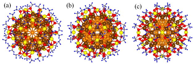
The Au144(SCH3)60 structural model obtained through the use of first-principles DFT optimization. Three orientations are shown, viewed along the following symmetry axes: (a) 5-fold axis, (b) 3-fold axis, and (c) 2-fold axis. The color scheme is that used in Fig. 1: inner core 54 Au atoms (orange), 60-atom outer shell (brown), 30 gold ad-atoms (yellow), and 60 sulfur atoms (red). The carbon and hydrogen atoms of the thiolate-tail are shown as small gray and blue spheres, respectively.
The construction and optimization of the structure model described above has been achieved through large-scale electronic structure theoretical calculations (based on density-functional theory, DFT), with structural relaxations performed without any constraints. In these calculations we have employed the ab-initio Born-oppenheimer molecular dynamics (AIBOMD) method which has been originally formulated19 for treating finite systems (charged or neutral), and the VASP DFT code20; for details see SI (section 2). Calculations applied to initial models constructed along the aforementioned principles, indeed resulted in energetically-optimized structures (one of which, for R = CH3, is illustrated and characterized in Figs. 1–3) that are fully I-symmetry compliant. Furthermore, the theoretically predicted structure posses a high degrees of order and symmetry as reflected by the sharply peaked distributions of interatomic distances and radial atomic shell radii shown in Fig. 3. This theoretically predicted structure model was used in the analysis of the measured data described in the following.
The reduced symmetry of the predicted structure model in comparison with some other common polyhedral structures, such as the icosahedral or the decahedral motifs, is reflected in the diffraction patterns at different orientations. A full map in reciprocal space is presented in Figure S3 of the SI. We compare those patterns with the experimental ones obtained from individual particles using STEM diffraction. The nanobeam diffraction (NBD) through the STEM imaging mode is controlled by the condenser lens system. The combination of probe-corrected STEM imaging and quasi-parallel beam diffraction (D-STEM) is obtained by positioning the beam in the STEM image at a single nanoparticle using the Digiscan control. The scan is stopped and positioned arbitrarily at a xy position on the screen. Subsequently, the electron diffraction pattern is recorded using a digital charge couple device (CCD) camera. D-STEM mode works in the diffraction plane, the overlapping of the convergent disks is optimized by a compensation of the last condenser lens (C3) and the use of the adaptor lens (ADL) at the hexapole coils of the CEOS corrector. Iteratively, the beam is aligned by adjusting the tilt and shift deflectors in order to reduce the disk radius in the convergent pattern into spot reflections.
Key to the success of our method is the use of a reduced (80 kV) accelerating voltage in the microscope. This is essential in order to minimize radiation damage of the nanocluster by the incident beam. Parallel-beam diffraction with nm-sized coherent probe in STEM is the only way for recording reciprocal space data from individual nanoclusters. The convergent beam angle is modified by changing the focal lengths of the condenser lens and the adaptor lens of the probe-corrector. Energy reduction to 80 kV in the STEM reduces significantly the radiation damage in the clusters. Diffraction modes in conventional TEM (convergent beam, selected area or nanodiffraction) have two important limitations: radiation damage may be significant, even when using low voltages, and the acquisition of precise electron diffraction (ED) data from individual clusters is problematic. In STEM mode we benefit from reduced damage due to the improvement of the probe size compared with TEM (probe-corrected). Further, the data collection is performed in a field of view that includes several isolated clusters. Subsequently the scanning is stopped and the collected ED data are recorded with a CCD camera (as videos) from all the clusters collected in the STEM-image (using the high-angle annular dark field detector). Changes in the beam size only modify the g-vectors of the reflections and their diameters. In order to measure these g-vectors (reciprocal space), we calibrate the CCD camera under exactly the same conditions as used for the clusters, but this time with a silicon [110] standard. The calibration of the electron diffraction patterns leads to errors minor than 0.01 nm.
Atomic resolution is not obtained under these conditions because the changes in the condenser lens; however the beam size is thin enough to detect individual clusters as we shown in Fig. 4. The electron diffraction patterns obtained in NBD-STEM preserve the symmetries of the clusters. These symmetries in the experimental and simulated patterns are employed in comparing the patterns with the use of the following aspects: number of reflections (first and second order), angles, distances, and relationship between g-vectors in the patterns. We note here that the symmetries of the clusters in the recorded data are preserved even when there are variations in the spot size. Using this methodology we were able to acquire images during ~20 sec before the sample was damaged, its structure altered irreversibly by the electron beam. In addition, in STEM nanodiffraction, we defocus the beam to a larger size, which allows for a much higher observation time of a single particle diffraction pattern without altering its crystal structure. As illustrated in Figure 4 (an image extracted from video 1 available in the SI), we focus the beam on a particle and subsequently move it to a nearby one. Since the particles are randomly oriented with respect to the electron beam, by exploring a large number of nanoparticles we can obtain a full plot in 3-D of the nanoparticles in reciprocal space.
Figure 4.
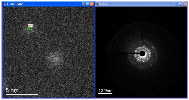
Example of STEM diffraction. The beam is located on the particle as shown on the left and the diffraction pattern is recorded subsequently. It is possible to move the beam to other particles. The particles do not show atomic resolution because of the way the beam is set to produce diffraction in which the spots do not overlap. This image was extracted from video 1, available in the SI.
We can compare the experimental patterns to the theoretical ones calculated using a model which can be refined to fit the experimental diffraction patterns, see Fig. 5. In quantitative comparisons between calculated and experimental patterns, we employ a number of criteria including: a) all spots on the experimental pattern are accounted for and correspond to calculated ones; b) angles between reflections should match with a 10% of error, with the error measured in the experimental and simulated reflections range from zero to a maximum of 2 degrees; and c) for every pattern diffraction pattern we also match the corresponding HAADF –STEM image and its FFT. As aforementioned, prior to this comparison, the experimental patterns were calibrated with a silicon [110] standard sample and the g-vectors in the clusters were obtained with an agreement of 0.01 nm in real space.
Figure 5.
Comparison between experimental and theoretical electron diffraction patterns. In these patterns a projection with 16 reflections is observed. (a) Experimental NBD pattern and (b) simulated electron diffraction pattern.
The results for the Au144SR60 cluster, displayed in Figure 5 for a number of orientations, show remarkable agreement between the measured and theoretically calculated patterns. The electron scattering or diffraction originates from interference among all the atoms in the structure. However, the brightest spots come from the atomic structure of the core, and the distances of the first reflections [(111) in fcc notation] are between 2.26 Å and 2.44 Å as predicted by the optimized structure model. We also observed spots in the interval 2.47–2.49 Å. We assign those to diffraction from gold atoms attached to sulfur atoms (that is the Au atoms in the stapling RS-Au-SR units) and the gold atoms on the surface of the grand core of the cluster (i.e. the 60-gold atom shell, see atoms colored brown in Fig. 1), which as predicted by the optimized structure model exhibit stretched bond distances. The model calculated and used to obtain the electron diffraction patterns has been encapsulated in a Cartesian box using the conventional Miller indices; in this way the cluster can be considered as a particle contained in a subspace from that <UVW> coordinates. Simulations of electron diffraction patterns were made using the SimulaTEM software package.21 We consider six different directions to rotate the simulated patterns: <100>, <010>, <1–10>, <110>, <111> and <112>, each from zero to 360 degrees; see the map illustrated in the Figure S3 of the SI. The whole set of electron patterns simulated were integrated in a stack of images and processed to create videos 2 to 7 in the SI. It is clear that due to the reduced symmetry of the structure the diffraction patterns repeat themselves many times. Unlike an infinite crystal nanoclusters in this size show only a limited number of different diffraction patterns.
If we keep the beam stationary on a particle, we observe that the diffraction pattern starts to change. Indeed, it is well documented that the electron beam produces rotations in clusters, which are reflected in contrast changes.22–24 However, tilting of the particle away from a low-index orientation will broaden the spot and increase the error in the measured angle. In our case, we noted that the patterns would show various orientations of the map of Figure S3 of the SI, and then after several seconds the diffraction pattern starts to change. We interpret this as the possibility that the sulfur–gold bonds on the capping layer are altered or broken by radiation damage. After several more seconds of electron beam exposure, the core is affected and becomes a more ordered structure such as a full decahedral or fcc single crystal structure. We consider this as the point in which the cluster has been already altered by radiation damage. It is important to note that these observed structures do not reflect the original atomic arrangement of the cluster. Instead they correspond to an alteration of the structure by the electron beam. In any case, with a careful selection of proper operational parameters (including low beam voltage, beam defocusing, and reduced exposure times) we can collect reliable diffraction data (patterns) to allow extraction of structural information. We note here that we never observed the “periodic” oscillations reported recently for uncapped clusters.25
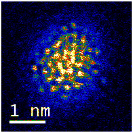
We also obtained images of the clusters with atomic resolution using the STEM-HAADF with a probe corrected electron microscope. We compared calculated images based on the theoretical model with experimental ones. The result is shown in Figure 6 for a number of images. We also included a comparison of its corresponding fast Fourier transform (FFT). Similar to the electron diffraction patterns in NBD-STEM and the simulations, we found a remarkable agreement confirming the correctness of the optimized structural model. Figure 6(a) shows one atomic-resolution HAADF-STEM image of a single Au144(SR)60 cluster obtained at 80 kV; Figure 6(a*) corresponds to its FFT. A simulated HAADF-STEM image is shown in Fig. 6(b) and its corresponding electron diffraction pattern Fig. 6(b*). We note here that the reduced quality of the FFTs, whether experimental or simulated, is caused by the use of a projected image in 2D; the FFTs of those high resolution images contain high frequencies that originate from the finiteness of the nanocrystal as well as the the finite number of pixels in isolated particles. The orientation of that cluster is near to a particular position (<110> angle 80) used for simulations displayed in Fig. S3 and shown in the videos included in SI. The HAADF-STEM simulated image has been obtained by employing the QSTEM software package26 using parameter values matching the experimental operational conditions of the aberration-corrected microscope. Since the DFT calculations to do not include thermal effects, we have employed the appropriate Debye–Waller factors in our simulations of the data.
Figure 6.

(a) Atomic resolution HAADF-STEM image of one Au144(SR)60 cluster and (b) the simulated HAADF-STEM image oriented 80 degrees in the [110] direction. (a*) and (b*) images correspond to the FFTs of (a) and (b) images, respectively.
It is desirable to quantify the comparisons between simulated and measured data, with the use of a reliability factor (R-factor) similar to the one defined in X-ray diffraction. However, in electron diffraction the intensity of a spot is not related simply to the square of the structure factor because of dynamical effects; some reflections might not be simply related to the atomic positions. Also, measurement of intensities is difficult because of the nonlinearity of the detectors. The small volume of the cluster produces few reflections, even with a good calibration of the gain in the CCD camera; and intensities cannot be used in a straightforward manner like in X-ray diffraction. This is a result of the size and the flatness of the Ewald sphere in electron diffraction. It is pertinent to remark here that our method is based on quantitative comparisons of the spot positions and angles. The ability of our method to probe individual clusters rather than data recorded as an average, over a crystal containing a large number of clusters, as in X-ray diffraction (even with bright synchrotron sources), provides the impetus for further development of the methods of data acquisition and quantitative data analysis.
In summary, we have shown here that a combination of STEM single particle diffraction with atomically resolved images obtained through the use of STEM-HAADF, in conjunction with calculation of images and patterns based on structure models obtained and optimized via theoretical first-principles (DFT) methods, can be used for the solution of the structure of thiolated clusters. We demonstrated this promising methodology through its application to a long-standing challenging problem – namely, the structure determination of the Au144(SR)60 nanocluster.
Supplementary Material
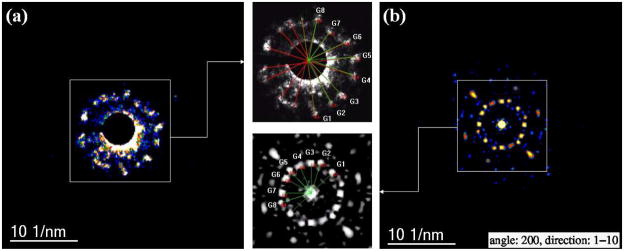
Table 1.
Measurements comparing experimental NBD-STEM and simulated electron diffraction patterns showed in Fig. 5.
| Spot | Angle(degrees) ±2 (error) | |
|---|---|---|
| Experimental | theoretical | |
| G1 | 24 | 25 |
| G2 | 16 | 17 |
| G3 | 25 | 23 |
| G4 | 20 | 19 |
| G5 | 21 | 18 |
| G6 | 26 | 27 |
| G7 | 23 | 19 |
| G8 | 22 | 25 |
Acknowledgments
This project was supported by grants from the National Center for Research Resources (5 G12RR013646-12) and the National Institute on Minority Health and Health Disparities (G12MD007591) from the National Institutes of Health. The authors would like to acknowledge to the NSF for support with grants DMR-1103730, “Alloys at the Nanoscale: The Case of Nanoparticles Second Phase and PREM: NSF PREM Grant # DMR 0934218; “Oxide and Metal Nanoparticles- The Interface Between Life Sciences and Physical Sciences”, The MALDI TOF/TOF work is supported by the National Science Foundation under CHE – 1126708. The work of B.Y. and U.L. was supported by the Office of Basic Energy Sciences of the US Department of Energy under Contract No. FG05-86ER45234, and in part by a grant from the Air Force Office of Scientific Research. Computations were made at the GATECH Centre for Computational Materials Science.
Footnotes
Notes
The authors declare no competing financial interest.
All the experimental details for synthesis and characterization, UV/Vis spectrum, MALDI-MS, theoretical model simulations, experimental NBD video and simulated electron diffraction pattern map and video is included in supporting information. This material is available free of charge via the internet at http://pubs.acs.org.
References
- 1.Billinge SJL, Levin I. The Problem with Determining Atomic Structure at the Nanoscale. Science. 2007;316:561–565. doi: 10.1126/science.1135080. [DOI] [PubMed] [Google Scholar]
- 2.Tran NT, Powell DR, Dahl LF. Nanosized Pd145(CO)x(PEt3)30 Containing a Capped Three-Shell 145-Atom Metal-Core Geometry of Pseudo Icosahedral Symmetry. Angew Chem, Int Ed. 2000;39:4121–4125. doi: 10.1002/1521-3773(20001117)39:22<4121::aid-anie4121>3.0.co;2-a. [DOI] [PubMed] [Google Scholar]
- 3.Jadzinsky PD, Calero G, Ackerson CJ, Bushnell DA, Kornberg RD. Structure of a Thiol Monolayer-Protected Gold Nanoparticle at 1. 1 Å Resolution. Science. 2007;318:430–433. doi: 10.1126/science.1148624. [DOI] [PubMed] [Google Scholar]
- 4.Love JC, Estroff LA, Kriebel JK, Nuzzo RG, Whitesides GM. Self-Assembled Monolayers of Thiolates on Metals as a Form of Nanotechnology. Chem Rev. 2005;105:1103–1169. doi: 10.1021/cr0300789. [DOI] [PubMed] [Google Scholar]
- 5.Qian H, Jin R. Controlling Nanoparticles with Atomic Precision: The Case of Au144(SCH2CH2Ph)60. Nano Lett. 2009;9:4083–4087. doi: 10.1021/nl902300y. [DOI] [PubMed] [Google Scholar]
- 6.Daniel MC, Astruc D. Gold Nanoparticles:3 Assembly, Supramolecular Chemistry, Quantum-Size-Related Properties, and Applications Toward Biology, Catalysis, and Nanotechnology. Chem Rev. 2004;104:293–346. doi: 10.1021/cr030698+. [DOI] [PubMed] [Google Scholar]
- 7.Whetten RL, Khoury JT, Alvarez MM, Murthy S, Vezmar I, Wang ZL, Stephens PW, Cleveland CL, Luedtke WD, Landman U. Nanocrystal Gold Molecules. Adv Mater. 1996;8:428–433. [Google Scholar]
- 8.Whetten RL, Price RC. Nano-Golden Order. Science. 2007;318:407–408. doi: 10.1126/science.1150176. [DOI] [PubMed] [Google Scholar]
- 9.Jin R. Quantum Sized, Thiolate-Protected Gold Nanoclusters. Nanoscale. 2010;2:343–362. doi: 10.1039/b9nr00160c. [DOI] [PubMed] [Google Scholar]
- 10.Tang Z, Robinson DA, Bokossa N, Xu B, Wang S, Wang G. Mixed Dithiolate Durene-DT and Monothiolate Phenylethanethiolate Protected Au130 Nanoparticles with Discrete Core and Core-Ligand Energy States. J Am Chem Soc. 2011;133:16037–16044. doi: 10.1021/ja203878q. [DOI] [PubMed] [Google Scholar]
- 11.Qian H, Eckenhoff WT, Zhu Y, Pintauer T, Jin R. Total Structure Determination of Thiolate-Protected Au38 Nanoparticles. J Am Chem Soc. 2010;132:8280–8281. doi: 10.1021/ja103592z. [DOI] [PubMed] [Google Scholar]
- 12.Heaven MW, Dass A, White PS, Holt KM, Murray RW. Crystal Structure of the Gold Nanoparticle [N(C8H17)4][Au25(SCH2CH2Ph)18] J Am Chem Soc. 2008;130:3754–3755. doi: 10.1021/ja800561b. [DOI] [PubMed] [Google Scholar]
- 13.Zhu M, Aikens CM, Hollander FJ, Schatz GC, Jin R. Correlating the Crystal Structure of A Thiol-Protected Au25 Cluster and Optical Properties. J Am Chem Soc. 2008;130:5883–5885. doi: 10.1021/ja801173r. [DOI] [PubMed] [Google Scholar]
- 14.Zeng C, Qian H, Li T, Li G, Rosi NL, Yoon B, Barnett RN, Whetten RL, Landman U, Jin R. Total Structure and Electronic Properties of the Gold Nanocrystal Au36(SR)24. Angew Chem. 2012;124:13291–13295. doi: 10.1002/anie.201207098. [DOI] [PubMed] [Google Scholar]
- 15.Brust M, Walker M, Bethell D, Schiffrin DJ, Whyman R. Synthesis of Thiol-Derivatised Gold Nanoparticles in a Two-Phase Liquid–Liquid System. J Chem Soc, Chem Commun. 1994:801–802. [Google Scholar]
- 16.Wong OA, Heinecke CL, Simone AR, Whetten RL, Ackerson C. Ligand symmetry-equivalence on thiolate protected gold nanoclusters determined by NMR spectroscopy. Nanoscale. 2012;4:4099–4102. doi: 10.1039/c2nr30259d. [DOI] [PubMed] [Google Scholar]
- 17.Lopez-Acevedo O, Akola J, Whetten RL, Gro3nbeck H, Ha3kkinen H. Structure and Bonding in the Ubiquitous Icosahedral Metallic Gold Cluster Au144(SR)60. J Phys Chem C. 2009;113:5035–5038. [Google Scholar]
- 18.Williams R. The Geometrical Foundation of Natural Structure: A Source Book of Design. Dover Publications; 1979. [Google Scholar]
- 19.Barnett RN, Landman U. Born-Oppenheimer Molecular-Dynamics Simulations of Finite Systems: Structure and Dynamics of (H2O)2. Phys Rev B. 1993;48:2081–2097. doi: 10.1103/physrevb.48.2081. [DOI] [PubMed] [Google Scholar]
- 20.Kresse G, Joubert D. From Ultrasoft Pseudopotentials to the Projector Augmented-Wave Method. Phys Rev B. 1999;59:1758–1775. [Google Scholar]
- 21.Gómez-Rodríguez A, Beltrán-del-Río LM, Herrera-Becerra R. SimulaTEM: Multislice Simulations for General Objects. Ultramicroscopy. 2010;110:95–104. doi: 10.1016/j.ultramic.2009.09.010. [DOI] [PubMed] [Google Scholar]
- 22.Williams P. Motion of Small Gold Clusters in the Electron Microscope. Appl Phys Lett. 1987;50:1760–1762. [Google Scholar]
- 23.Ben-David T, Lereah Y, Deutscher G, Penisson J, Bourret A, Kofman R, Cheyssac P. Correlated Orientations in Nanocrystal Fluctuations. Phys Rev Lett. 1997;78:2585–2587. [Google Scholar]
- 24.Be’er A, Kofman R, Phillipp F, Lereah Y. Spontaneous Crystallographic Instabilities of Pb Nanoparticles in a SiO Matrix. Phys Rev B. 2007;76:075410. [Google Scholar]
- 25.Wang ZW, Palmer RE. Experimental Evidence for Fluctuating, Chiral-Type Au55 Clusters by Direct Atomic Imaging. Nano Lett. 2012;12:5510–5514. doi: 10.1021/nl303429z. [DOI] [PubMed] [Google Scholar]
- 26.Koch CT. Ph D Thesis. Arizona State University; 2002. Determination of Core Structure Periodicity and Point Defect Density Along Dislocations. [Google Scholar]
Associated Data
This section collects any data citations, data availability statements, or supplementary materials included in this article.