Abstract
A dedicated analytical scanning transmission electron microscope (STEM) with dual energy dispersive spectroscopy (EDS) detectors has been designed for complementary high performance imaging as well as high sensitivity elemental analysis and mapping of biological structures. The performance of this new design, based on a Hitachi HD-2300A model, was evaluated using a variety of biological specimens. With three imaging detectors, both the surface and internal structure of cells can be examined simultaneously. The whole-cell elemental mapping, especially of heavier metal species that have low cross-section for electron energy loss spectroscopy (EELS), can be faithfully obtained. Optimization of STEM imaging conditions is applied to thick sections as well as thin sections of biological cells under low-dose conditions at room- and cryogenic temperatures. Such multimodal capabilities applied to soft/biological structures usher a new era for analytical studies in biological systems.
1. Introduction
Following the development of field emission electron sources by Crewe [1], the spatial resolution of scanning transmission electron microscopy (STEM) has since been greatly improved, and it has been applied to study biological structures for both imaging and mass determination since the 1970s [2-4]. Recently, improved specimen preparation techniques, low dose methodologies and related practical developments have significantly advanced “imaging” applications of STEM for biological materials, including 3-D tomography and absolute mass determination of macromolecules [5]. STEM imaging is superior for thick sections of biological samples in terms of enhanced contrast over conventional transmission electron microscopy (TEM), as demonstrated in the reconstruction of a human erythrocyte by axial STEM tomography [6] as well as improved spatial resolution given minimal influence of chromatic aberration in STEM mode of imaging, particularly at lower operating energies. With an annular dark-field detector, STEM collects electrons scattered at predefined high angles for image formation, while simultaneously allowing small-angle scattering electrons to pass through the opening in the detector to an electron energy-loss spectrometer (EELS). Its ability to perform both multimodal imaging and spectroscopy makes STEM a truly powerful analytical approach for studying biological materials [7-8]. This approach allows determination of elemental compositions at the subcellular levels with high quantitative accuracy and spatial resolution, however several particularly important unmet needs are emerging at the interfaces of bioinorganic chemistry, biology, medicine and material science.
Until recently, analytical accessories for biological STEM have often been limited to energy-filtered imaging and EELS spectroscopy/mapping for only handful suitable elements that offer a high cross-section for EELS (e.g., Ca, Fe). Although an x-ray energy-dispersive spectroscopy (EDS) detector can also be attached to study the compositional distribution in cells [9], chemical analysis and mapping of biological specimens via EDS in STEM is limited by specimen stability considerations and poor geometric collection efficiency of x-rays, thus the resultant inadequate analytical sensitivity for biologically relevant metals.
With the emerging recognition of the regulatory roles for fluxes in the concentrations of metal complexes (e.g., Zn, Fe, Mn and Cu) and metalloproteins in biology [10-12] and the concomitant need for high analytical sensitivity in EDS, we have designed and developed a dedicated cryo-compatible biological STEM for analytical studies of biological materials and molecular structures. The new instrument is based on the Hitachi HD-2300A model, equipped with all the traditional high sensitivity electron detectors and significantly reduced radiation damage with a controlled weak probe current (as small as 7 pA), fast scanning, and cryo-compatible operation in low-dose modes. More importantly, the new STEM is equipped with a dual-EDS system with two separately positioned yet integrated EDS detectors (each with ∼0.38 sr. nominal collection angles), thereby greatly improving the elemental sensitivity and minimum detectability limits for relevant metals. The dual EDS detector system comprises two Si(Li) detectors from Thermo Fischer Scientific with beryllium windows and 25 degree take-off angle which are run in parallel and achieve a typical energy resolution of 138 eV.
The analytical sensitivity for EDS is often characterized by a minimum mass fraction (MMF), which is related to peak intensity, the peak-to-background ratio and the collection time [13]. For a given sample concentration and collection time, one must increase either count rate or the peak-to-background ratio to increase the analytical sensitivity. Given a robust sample, it is possible to increase the beam current or beam current density (through e.g. aberration correction) to achieve higher count rates [14]; however, for biological structures, tissues and other beam-sensitive materials, it is necessary to use a moderate beam current to avoid sample damage. We demonstrate the expected doubling of peak intensity, thus the analytical sensitivity, with the dual-EDS detector system with ∼0.76 sr nominal collection angle, when compared to a single detector implementation. Hard x-rays and stray electrons in the microscope column have a strong influence on the peak-to-background ratio. These effects are characterized in the dual-EDS STEM with the standard NiO test specimen to demonstrate the excellent analytical performance of this system. The instrument is naturally compatible with electron energy loss spectroscopy (EELS) and STEM imaging for simultaneous imaging and chemical analysis. While Norans software was used for EDS quantitative analysis, we selected different quantification methods for samples with different thickness, i.e. ZAF method for thick, single cell sample, while Cliff-Lorimer method for thin sections.
While the ultimate resolution of STEM is determined by the probe size (nowadays approaching sub-angstrom through aberration correction), the actual (practical) resolution achieved in biological sample is restricted by the applied electron dosage (for given beam energy) when an image with reasonable signal-to-noise ratio can be recorded before the sample is damaged. The maximum dose a molecule can tolerate before unacceptable degradation happens is mainly dependent on chemical effects of the electron irradiation on the molecule and the nature of the biological/molecular material. For large protein molecules, the critical damage dose above which a single molecule is damaged per prior literature is about 5 e−/Å2[15-16]. It has also been estimated that at least 10,000 molecules are needed to build a 3-dimensional structure at ∼3Å resolution by cryo-electron microscopy with samples maintained at/about liquid nitrogen temperature [15-16]. In conventional STEM imaging conditions without any lens aberration correction (i.e. a beam current of ∼300 pA, a pixel dwell time of 10 μs/pixel and a pixel size of 1.75 Å2), the electron dose is about 1×10⁴ e−/Å2, which is about 2000-fold higher than that required to preserve the structure of biomolecules. Compared to low-dose cryo-TEM where high resolution can be obtained at low-dose condition, e.g. 1.6 Å resolution at 1 to 10 e−/Å2[17], high resolution low-dose STEM for the study of biological samples is not well developed or fully understood [18].
Calculations have shown that under the same electron dose and image contrast, TEM phase contrast microscopy has better a signal to noise ratio than annular dark-field STEM [19]. In the HD-2300A STEM, images can be captured simultaneously by bright-field (phase contrast) and annular dark-field detectors (mass/thickness contrast for mass measurement), where useful information may be obtained by the two complementary images. We have designed a control of STEM low-dose operation on the microscope: i.e., switching between search mode from one area in low magnification (about 2-10 K) to imaging mode in another pre-defined area at high magnification without affecting the alignment of any lenses. Tobacco mosaic virus (TMV) viruses were then used as the test sample to demonstrate the cryo-STEM capability of the Hitachi STEM, where high contrast images can be recorded in combination with appropriate sample preparation methods.
2. Materials and methods
Some of the cell samples were prepared by conventional methods: fixations, staining, dehydration, embedding in resin and sectioning to obtain thin slices observed at room temperature. To analyze the whole cell samples, freeze-drying was used to preserve the overall cell morphology and architecture. Here, the unstained sample was adsorbed onto a carbon film about 20 nm thick, plunge-frozen, freeze–dried in a Turbo-pumped freezing-dryer and observed in the STEM at room temperature. For cryo-STEM experiments, the samples were plunged into liquid ethane using a plunge freezer (Gatan) and transferred into the HD-2300A STEM via the Gatan cryo-transfer station. A special Gatan cryo-holder with two side-cuts fitting aligned towards the two EDS detectors was used in the cryo-STEM. For EDS performance characterization, a nominal NiO test specimen (Ted Pella, Inc) was used; which consists of a ∼56 nm NiO film on a ∼20 nm amorphous carbon film supported by a 200 mesh Mo grid. The test specimen was cleaned in Ar plasma prior to testing and mounted in a specially designed dual cut-out low background holder. As the two EDS detectors are mounted on opposite sides of the column, all tests were performed near the center of the grid with close to 0° sample tilt. The performance of the detectors was characterized at 80, 120 and 200 kV in normal mode with condenser aperture of 50 um, which resulted in a probe current of approximately 84, 128 and 295 pA, respectively. The spectra were collected from a 90×90 nm2 area with acquisition time of 200 seconds. The total electron doses applied in 200 seconds were 1.3×10⁵, 2.0×10⁵ and 4.5×10⁵ e−/Å2, respectively for 80, 120 and 200 kV.
3. Results and discussion
3.1. Complementary STEM images collected by SE and bright- and dark detectors
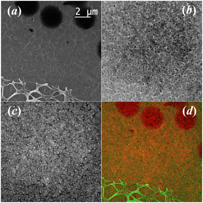
The dedicated dual-EDS Hitachi HD-2300A STEM has a secondary electron (SE) detector located above the sample so it can readily function as a high-voltage and high-resolution scanning electron microscope (SEM). With this SE detector, biological cells and tissues of thicknesses in the range of micron and above can be readily examined by detecting SE (or BSE) signals generated from their surfaces. The SE images can be obtained simultaneously to other STEM images collected by bright-field and dark-field detectors. Fig.1 (a) shows an SE image of a porous hydrogel sample formed by protein crosslinking, where STEM sample was prepared by the freeze-drying method. The surface is not flat but filled with large holes (some larger than 2 μm in diameter) as shown by arrowheads in Fig.1 (a), while a piece of broken carbon film used as the supporting film can also be seen in the bottom of the figure. However, the internal pores embedded inside the gel could not be revealed until the sample was imaged by transmitted electrons with bright-field and dark-field detectors underneath the sample.
Figure 1.
STEM images of protein gel collected on HD-2300A by different detectors: (a) secondary electron (SE) detector; (b) Z-contrast (ZC) annual dark field detector and (c) TE (transmission electron) bright-field detector, from the same area. While SE image shows the surface morphology, ZC and TE reveal the poles inside the structure. (d). A color mixed image of (a) and (c) showing both the surface and internal structure of the protein gel. The electron dose for imaging is about 4 e−/Å2 per frame (200 kV, 50 um condenser aperture, probe current of 295 pA, pixel dwell time of 30.5μs and pixel size of 169 nm2).
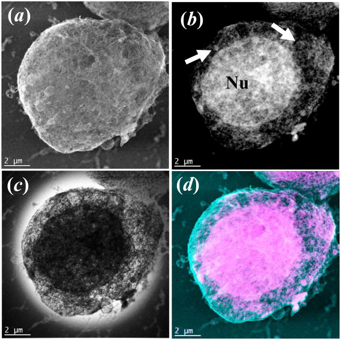
Fig.1 (b) is the STEM image of the same gel collected with the annular dark field detector where the internal pores appear dark, while they appear bright in the bright-field STEM image of Fig.1(c) due to the obvious mass thickness contrast. The average size of the internal pores was measured to about 200 nm. A more informative view of the gel sample can be obtained if the surface morphology shown in fig. 1(a) is combined with its internal structure (Fig.1c), as shown in Fig. 1(d), which is a mixed pseudo-color representation of both images. As another example, a Jurkat cell sample was attached to a formvar/carbon coated grid, plunge-frozen in liquid ethane, and freeze–dried before examination in the HD-2300A. The STEM images of the Jurkat cell collected by SE, bright-field and dark-field detectors are shown in Fig.2 (a), (b) and (c), respectively. Fig.2 (d) is a pseudo-colored representation of the Jurkat cell imaged with SE and dark-field, where both, surface and internal features can be readily seen. With conventional TEM, internal features are only visible in sections or in fractured samples of cells, while the surface can only be imaged with SEM of intact cells (i.e. non-sectioned and non-fractured). The significance of Figure 2(d) is that we can simultaneously observe the surface as well as internal features of the same whole cell. This makes it possible for us to differentiate between cells in interphase and cells in mitosis. While interphase cells have a clearly recognizable nucleus (as shown in the figure), the nucleus is not present in dividing cells during the metaphase of the cell cycle, when the DNA in condensed into chromosomes. Also, the additional information from the SE image allows us evaluate the overall integrity of the cell plasma membrane, which is not achievable with transmitted electron imaging alone.
Figure 2.
STEM images of a Jurkat cell collected on HD-2300A by different detectors: (a) secondary electron (SE) detector; (b) Z-contrast (ZC) annular dark field detector, and (c) TE (transmission electron) bright-field detector, (d) is an overlay of the colorized ZC and SE image. While in (a) the surface of the cell is visible, the images in (b) and (c) reveal the nucleus (Nu) and organelles in the cytoplasm (arrows in b). The electron dose for imaging is about 8 e−/Å2 per frame (200 kV, 75 um condenser aperture, probe current of 691 pA, pixel dwell time of 30.5μs and pixel size of 156 nm2).
This unique combination of high-energy SE imaging coupled to conventional STEM BF/ADF and HAADF imaging modes provides versatility for imaging both surface and internal sub-structure with this instrument.
3.2. Dual-EDS Performance
The analytical performance of the dual-EDS STEM instrument was characterized with a NiO test specimen supported on molybdenum grid as outlined by Bennett and Egerton [20]. First, the matching and simultaneous operation of the two detectors was verified by sequential collection of EDS spectra as shown in Fig. 3. The figure shows the matching of the two EDS detectors and the expected doubling of integrated peak intensity for a 200 s acquisition with about 300 pA beam current. The peak-to-background ratio was calculated using the standard Fiori method (P/B10) [21] and found to be ∼2400. To estimate the contribution of hard x-rays and scattered electrons in the system, we collected both film-count ratio (FCR) and hole-count ratio (HCR) data. The FCR is the ratio of the background subtracted Ni-Kα peak from the film to the Mo-Kα peak from the grid. Spectra collected from near the center of the grid opening yielded the FCR data shown in fig. 4, which increases with beam energy due to lower scattering in the specimen. Both the FCR and P/B10 data collected compare to the highest published values from a round-robin study [20]. The HCR data (similar to FCR, but denominator is from a region with no film) shown in fig. 5 illustrates the strong beneficial effect of the thick (1.0 mm) Pt EDS aperture, particularly at 80 keV.
Figure 3.
Portion of spectrum from NiO sample showing detector matching and doubling of peak intensity in the two detector configuration.
Figure 4.
Film-count ratio (FCR) data from NiO test specimen at 80, 120 and 200 keV.
Figure 5.
Hole-count ratio (HCR) data from NiO test specimen at 80, 120 and 200 keV.
3.3. The Whole Cell EDS Mapping and Analysis
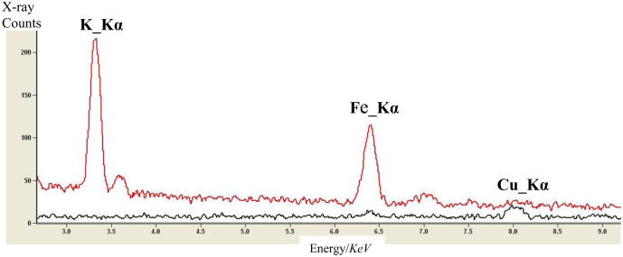
The interaction volume of x-ray generation in EDS becomes larger in bulk specimens with higher accelerating voltage, i.e. the maximum sampling depth can be up to about 20 μms at 80 kV when simulated by Monte Carlo algorithm for pure carbon material. Thus, EDS analysis is quite appropriate to study the composition of the whole cell samples with thickness in the range of few μms, especially with the dual-EDS system on our Hitachi STEM. For example, the levels of K, Fe and Zn within the red blood cell have great implications for cell growth and function. We collected EDS spectra from a human RBC and compared to those of background; that was collected from the surrounding area closer to the cell, as shown in Fig.6. Quantitative analysis of the spectra collected from 11 different cells with absorption correction shows the averaged and normalized Fe:Cu:Zn atomic ratio of 31.8 : 4.0 : 0.7. The average Fe content of human RBCs is ∼2.41 fmole/cell [12]. Based on this, the levels of Cu and Zn are calculated to be 0.30 and 0.05 fmole/cell respectively. This level of Cu is higher than published values, wherein Cu and Zn are 0.0008 fmol/cell and 0.02 fmol/cell, respectively [12]. The excess Cu is likely not from the Mo and nylon grids used in the experiments, but rather from the copper cover on the holder. There are no Cu peaks present in the hole-count spectrum.
Figure 6.
Comparison of EDS spectra collected from center of the cell as marked by rectangle 1 and from the area outside the cell marked as rectangle 2 in fig. 7(a). The Kα peaks of K, Fe and Cu are labeled. This confirms that K and Fe signals are mainly from the cell, while Cu signal is from the holder.
Additional and more useful information can be derived from spatial distribution of chemical species across various cellular and sub-cellular compartments. The red blood cell is quite flexible, which may change its shape during blood transport. Figure 7 (a) shows a dark-field STEM image of a RBC with such deformation, as the most of the cell contents is shifted to the left. Figure 7 (b-d) show the EDS maps of K, Fe and Zn, respectively, collected from this RBC. It shows metal species distribute almost uniformly inside the cell. RBC under examination has a thickness of about 1-2 microns along the beam direction. With the NORAN software, the EDS maps were calculated by removing the background in the EDS spectra and separating the contributions of each selected element from overlapped peaks to provide net count.
Figure 7.
(a) STEM image of a red-blood cell collected by annular dark-filed detector, and dual-EDS x-ray mappings of the cell: (b) K; (c) Fe and (d) Zn maps, where Kα peak of the elements was used for the mapping. Rectangle 1 shows the area to collect the spectrum of the RBC cell, while rectangle 2 shows the area to collect the background spectrum, as shown in Fig.6. The electron dose is about 20 e−/Å2 per frame (200 kV, 75 um condenser aperture, probe current of 691 pA, pixel dwell time of 152 μs and pixel size of 324 nm2). The EDS map is built with accumulation of 176 frames.
3.4. EELS Analysis
We performed EELS elemental studies in ultrathin sections of mouse spermcells prepared by conventional methods (as described in Materials and methods). In the mass/thickness contrast STEM image collected by the dark-field detector, the head and mid-piece of the cells can be easily recognized, despite being unstained, as shown in fig. 8(a). EELS line scan were performed to study elemental distribution crossing the line shown in fig. 8(a). Fig.8 (b)-(d) show the elemental profiles of P, S and N across the line. It is clear that the P-, N, and S content in the head (concentrated with DNA and protamines) is much higher than that in other areas. The plasma membrane can also be pointed out corresponding to P peaks in the line profile, as indicated by black arrowheads in fig. 8(b). However, the signal noise ratio (SNR) of the P peaks showing the plasma membrane's locations was low. This might be due to the existence of P in the background (i.e. there are also P in the acrosomal material of sperm cells) and not adequate acquisition time restricted by specimen stability under electron beam irradiation. We performed EELS quantification by splicing and deconvoluting the spectra collected from the sperm head (the raw EELS spectra were shown in supplementary figures 1 to 4). The calculated ratio of N:P:S is 45:5:1, which is in the range of the values given in the literature 36:4:1 [22]. For comparison, we collected also EDS spectra from a thin section of mouse sperm cell, as shown in Supplementary Figure 5. We did quantitative analysis of the spectrum from a part of the sperm head and obtained the atomic ratio between P:S of 81:19. Since S content is low in the sperm head cell (∼1 %), the clear observation of S peak is also the other sign of high sensitivity. In order to achieve a large collection angle we used thick Be windows on the Thermo EDS detectors. Such thick windows, however, prevents us from collecting EDS signals from elements lighter than Na. In our current settings, N cannot be detected by EDS.
Figure 8.
(a) A high-angle dark-field STEM image of a thin section of mouse sperm cell, showing both head and midpiece sections. The white dotted line shows the region used for EELS spectra imaging. (b)-(d) show P, S and N profiles along the line, respectively. The arrows in (a) and (b) show the positions of the plasma membrane, where there is an increase of P. The calculated average thickness is about 54 nm measured by the zero-loss and plasmon peaks. The longitudinal section through the sperm head shows the acrosome (Ac) and the nucleus (Nu). Mitochondria (Mt) are present in the midpiece (Mp) only, while outer dense fibers (Odf) are visible in the tranversal sections of the midpiece (Mp) and the principal piece (Pp). The fibrous sheath (Fs) is seen in principal pieces exclusively. Note the decreasing diameter of the different sperm tail regions. The total electron applied for the line scan was about 6.3×10¹⁰ e− (80 kV, 50 um condenser aperture, probe current of 84 pA, pixel dwell time of 1 s, pixel size of 15 nm, 120 pixels in total for the line scan).
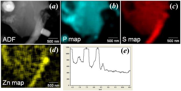
In another example of biological significance, we have examined the spatial distribution of zinc in male spermatozoa. As has been articulated in recent years, there is increasing evidence that zinc signaling is vitally important in many biochemical signaling processes, especially those at the onset and progression of fertilization of egg. The male reproductive system contains some of the most zinc-rich tissues in the body including the testis, epididymis, and prostate [23]. These tissues participate in the production, maturation, and ejection of the spermatozoa. The sperm cells themselves also are enriched in zinc; interestingly, the localization of histochemically reactive (labile) zinc changes throughout sperm maturation in the epididymis of the rat [24]. Elemental maps of mouse spermatozoa were similarly collected via EDS detection. Figure 9 shows ADF STEM image, and x-ray maps of P, S, and Zn, respectively. When the Zn_Kα map was calculated, a high precision, noise reduction filter has been applied; this leaded to the square pixilation appearance of the map. Their elemental maps confirm the known elemental signatures of these cells, such as the compartmentalization of phosphorus-rich DNA that is densely packed with sulfur-containing protamines in the sperm head [25].
Figure.9.
(a) Z-contrast Annual Dark field STEM image and x-ray mappings including (b) P, (c) S and (d) Zn maps of a sperm cell, where Kα peak of the elements was used. (e) The sum EDS spectra of the cell, where Zn peak can be seen. The electron dose is about 60 e-/Å2 per frame (200 kV, 75 um condenser aperture, probe current of 691 pA, pixel dwell time of 50 μs and pixel size of 36 nm2). The EDS map is built with accumulation of 205 frames.
3.5. Imaging of thick sections
STEM has the clear advantage for imaging thick sections. Compared to TEM, it has minimal chromatic aberration of the objective lens. Figure 10 shows mass/thickness contrast STEM images of unstained MIN6 Islet beta cells embedded in LR white resin. We have compared two sections: 60 nm as shown in Fig.10 (a) and 200 nm in (b), which clearly resolve key sub-cellular features, such as the nucleus and mitochondria, in both samples. Osmium tetroxide stained sections with a thickness of about 500 nm were also similarly imaged. Figure 11 shows a STEM image of a stained L540 Hodgkin's Lymphoma cancer cell embedded in LR White resin and sectioned to about 500 nm. Again, most of the cell components are easily resolved. Thus, imaging of thick sections of cells and tissues is greatly facilitated by STEM imaging, and the thickness can be readily optimized for improved contrast considerations.
Figure 10.
Z-contrast STEM image of uncontrasted MIN6 Islet beta cells embedded in LR White resin, (a) The thickness of the ultrathin section is ca. 60 nm, (b) of the thick section ca. 200 nm. The nucleus (Nu) with dense heterochromatin and less dense euchromatin, and mitochondria (arrows) are visible in both images. The electron dose is about 86 e−/Å2 per frame (200 kV, 75 um condenser aperture, probe current of 691 pA, pixel dwell time of 50 μs and pixel size of 25 nm2).
Figure 11.
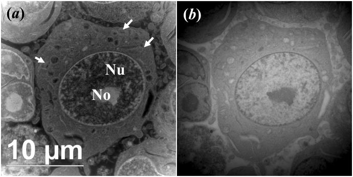
STEM image of OsO4 stained L540 Hodgkin's Lymphoma cancel cell embedded in LR White resin and sectioned to about 500 nm, collected by (a) annular dark-field detector and (b) bright-filed detector. The nucleus (Nu), nucleolus (No), and mitochondria (arrows) are indicated. The electron dose is about 4 e−/Å2 per frame (200 kV, 75 um condenser aperture, probe current of 691 pA, pixel dwell time of 50 μs and pixel size of 484 nm2).
3.6. Cryo-SEM and Cryo-STEM
With the secondary electron detector, the HD-2300A can be operated as a high-voltage scanning electron microscope. This makes it possible to imaging thick samples, i.e. even bulk samples with millimeter thickness can be studied using a Hitachi bulk specimen holder. Cryo-scanning electron microscopy (cryo-SEM) is a well established method to study morphology and surface structures of biological and organic materials with resolution down to few nanometers [26-28]. Here, the samples were prepared via fast freezing with a Gatan cry-plunge station similar to normal cryo-TEM. After the samples were transferred into the column, the specimen-holder temperature was increased to minus 120 degree to reduce the contamination and damage. Since the sample is positioned on a thin and conducting carbon film, the problem of charging is much less severe than true bulk samples. Figure 12 shows a high-voltage cryo-SEM image and the corresponding dark field and bright field images of a mouse sperm cell. The overall shape of the head and a part of the midpiece can be clearly seen and also the mitochondrial sheath of the midpiece is recognizable. Cryo-SE is especially useful to study samples with thickness more than a few microns, when it is not possible to image the structure using either bright-filed or dark-field detectors in typical S/TEM which collect the transmitted electrons.
Figure 12.
(a) A high-voltage cryo-secondary electron (SE) on HD-2300A: cryo-SE image of a frozen mouse sperm cell. The head and a part of the midpiece are shown. The mitochondrial sheath surrounding the midpiece of the tail is recognizable (arrows). The STEM images of the sperm collected by (b) dark-field detector, and (c) bright-field detector are shown for comparison. The electron dose for imaging is about 7 e−/Å2 per scan (200 kV, 75 um condenser aperture, probe current of 691 pA, pixel dwell time of 30.5 μs and pixel size of 196 nm2).
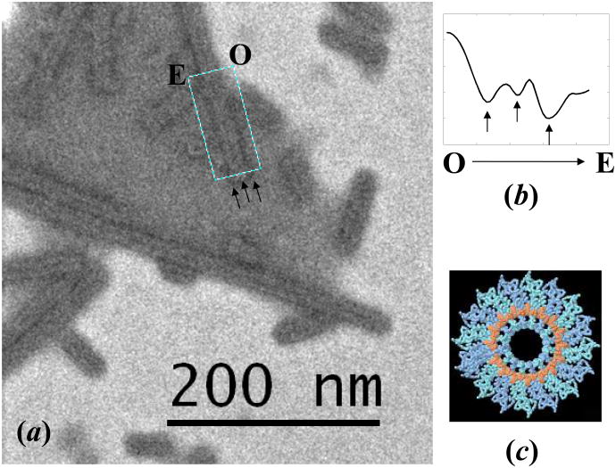
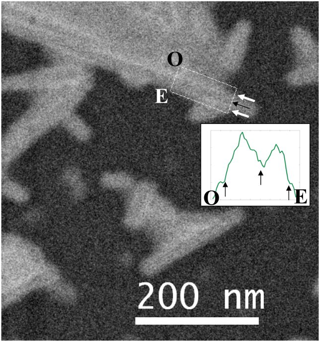
We have utilized typical tobacco mosaic virus (TMV) as the test sample to perform cryo-STEM under low-dose imaging conditions. The image shown in Fig.13 were taken using a high voltage of 80 kV with an electron dose at about 53 e−/Å2electron (84 pA beam current, a pixel dwell time of 10 μs/pixel and the pixel size of 98 Å2). The sample was prepared by cryo-plunging in liquid ethane, followed by freeze-drying inside the TEM column by raising the temperature to -120 degree. The phase contrast in a STEM image is lower than that of normal TEM under the same dosage; however, HAADF STEM and wide-angle bright-field STEM images show mass/thickness contrast. Figure 13 (a) is a wide-angle bright-field STEM image collected by the bright-field detector with a high collection angular range from zero to 30 mrad. Unlike normal mode, where the collection angle only ranges from zero to 3 mrad, the detector identifies a clear phase contrast besides some inversed mass/thickness contrast since some high-angle scattered electrons are also collected by the bright-field detector. It is well-known that TMV is a common helical virus with diameter of about 15-18 nm. Since there is no DNA, there is a low-density area in the center as shown in Fig.13(c), which is a projection of TMV virus along its helical axis. In Fig.13 (a), a thin dark line is observed in the center of the helix. The thin dark line can be clearly seen in the line profile shown in Fig.13(b), which corresponds to the interface between low-density at the core and the outer shell (mainly caused by phase contrast). Fig.14 shows a STEM image of the TMV virus, collected by a high-angle dark-filed detector, which show mass/thickness contrast. From the line profile of the TMV as shown in the insert in Fig.14, we can find that there is a dark line in the center, which is due to mass-thickness contrast with reduced scattering along the center. Such mass-thickness and phase contrast observed in STEM images for biological samples has clear and compelling applications in high resolution structural biology by proving supplemental information to structural reconstruction.
Figure 13.
(a) Cryo-STEM image of TMV virus collected by bright-field detector at wide-angle mode with a large collecting angle (up to 30 mrad). (b) An integrated line profile of the rectangular area shown in (a), from position O to E. Besides the two back lines corresponding to the edges of the TMV virus, a thin black line can also be found corresponding to the low-density center, as marked by the arrowheads. (c) is the structure of a TMV virus projected along the helical axis showing there is a low-density area in the center. The electron dose for imaging is about 53 e−/Å2 per scan (80 kV, 50 um condenser aperture, probe current of 84 pA, pixel dwell time of 10 μs and pixel size of 98 Å2).
Figure 14.
Cryo-STEM image of TMV virus collected by high-angle dark field detector. The insert is an integrated line profile of the rectangular area shown in the image, from position O to E. A thin black line can be found corresponding to the low-density center, as marked by the arrowheads. The electron dose for imaging is about 53 e−/Å2 per scan (80 kV, 50 um condenser aperture, probe current of 84 pA, pixel dwell time of 10 μs and pixel size of 98 Å2).
These representative examples encompassing diverse characterization of biological (and soft) structures underscore the efficacy and utility of Hitachi 2300A dual-EDS STEM for multimodal imaging and spatially resolved chemical mapping in biology and related soft matter. Table 1 summarizes the comparison of the dedicated STEM HD-2300A to a conventional biological transmission electron microscope.
Table 1.
Comparison of the HD-2300A STEM to a conventional bio-TEM.
| HD-2300 STEM | A Conventional Bio-TEM | |
|---|---|---|
| Imaging Capability | Secondary Electron (SE) Phase contrast STEM (bright-field detector) Diffraction contrast STEM (bright-field or dark-field detector) Z-contrast STEM (high-angle dark-field detector) |
Only phase and diffraction contrast TEM |
| Analytical Capability | High sensitive EDS EELS |
Normally only EELS, or none |
| Applicability | Thin and thick sections | Normally thin section at low kV. |
| Low-dose operation | Yes | Yes |
| Cryo-capability | Yes | Yes |
| Diffraction | CBED/nano-beam diffraction | Selected area electron diffraction |
| tomography | Yes | Yes |
| Instrument resolution | 0.3 nm | ∼0.3 nm |
4. Summary and conclusion
An analytical STEM equipped with EELS, dual-EDS configuration, cryo-compatibility, low-dose modalities has been designed and developed for multimodal imaging, spectroscopy and spectroscopic imaging of soft/biological structures. The utility and performance of imaging modes, EELS and dual-EDS characteristics of the instrument, which is based on standard Hitachi HD-2300A STEM model, have been assessed with model test structures and several biological samples. The doubling of collection angle for x-rays with dual-EDS geometry results in expected enhanced analytical sensitivity, particularly for biologically relevant element such as zinc, which is not possible by EELS given its poor edge definition and scattering cross-section. The whole-cell elemental mapping was demonstrated to be an effective method of resolving compositional distribution in biological cells. The other available complementary approach of EELS can be readily employed to identify light atoms in thin sections, and to determine the thickness of a whole red-blood cell. The low-dose, low-temperature STEM study of TMV virus showed useful mass/thickness contrast. We believe that development of such analytical STEM, particularly with the dual-EDS configuration, promises to open new vistas for understanding inorganic physiology: i.e. the critical interplay of metals, metalloids and main group species in biology by offering spatially resolved high-sensitivity element-specific mapping and analysis in biology.
Supplementary Material
Acknowledgments
Research was supported by the W. M. Keck Foundation Medical Research Award, a SPARK Award from the Chicago Biomedical Consortium and NIH and National Institutes of Health Grants GM038784 (O'Halloran), P01 HD021921 Project 3 (Woodruff). This work was performed in the EPIC facility of NUANCE Center and the QBIC facility in the Chemistry of Life Processes Institute at Northwestern University. The NUANCE Center is supported by NSF-NSEC, NSF-MRSEC, Keck Foundation, the State of Illinois and Northwestern University. The protein hydrogel sample was kindly provided by Prof. George Anne for testing at University of Chicago.
Footnotes
Publisher's Disclaimer: This is a PDF file of an unedited manuscript that has been accepted for publication. As a service to our customers we are providing this early version of the manuscript. The manuscript will undergo copyediting, typesetting, and review of the resulting proof before it is published in its final citable form. Please note that during the production process errors may be discovered which could affect the content, and all legal disclaimers that apply to the journal pertain.
References
- 1.Crewe A, Wall J, Langmore J. Science. 1970;168:1338. doi: 10.1126/science.168.3937.1338. [DOI] [PubMed] [Google Scholar]
- 2.Engel A. Ultramicroscopy. 1978;3:273. doi: 10.1016/s0304-3991(78)80037-0. [DOI] [PubMed] [Google Scholar]
- 3.Langmore JP, Wooley JC. Proc Natl Acad Sci USA. 1975;72:2691. doi: 10.1073/pnas.72.7.2691. [DOI] [PMC free article] [PubMed] [Google Scholar]
- 4.Woodcock CLF, Frado LLY, Wall JS. Proc Natl Acad Sci USA. 1980;77:4818. doi: 10.1073/pnas.77.8.4818. [DOI] [PMC free article] [PubMed] [Google Scholar]
- 5.Muller SA, Engel A. Chimia. 2006;60:749. [Google Scholar]
- 6.Hohmann-Marriott MF, Sousa AA, Azari AA, Glushakova S, Zhang G, Zimmerberg J, Leapman RD. Nature Methods. 2009;6:729. doi: 10.1038/nmeth.1367. [DOI] [PMC free article] [PubMed] [Google Scholar]
- 7.Colliex C, Mory C. Biol Cell. 1994;80:175. doi: 10.1111/j.1768-322x.1994.tb00928.x. [DOI] [PubMed] [Google Scholar]
- 8.Hunt JA, Disko MM, Behal SK, Leapman RD. Ultramicroscopy. 1995;58:55. [Google Scholar]
- 9.Gakh O, Adamec J, Gacy AM, Twesten RD, Owen WG, Isaya G. Biochemistry. 2002;4:6798. doi: 10.1021/bi025566+. [DOI] [PubMed] [Google Scholar]
- 10.Kim AM, Vogt S, O'Halloran TV, Woodruff TK. Nature Chemical Biology. 2010;6:674. doi: 10.1038/nchembio.419. [DOI] [PMC free article] [PubMed] [Google Scholar]
- 11.Kim AM, Bernhardt ML, Kong BY, Ahn RW, Vogt S, Woodruff TK, O'Halloran TV. ACS Chemical Biology. 2011;6:716. doi: 10.1021/cb200084y. [DOI] [PMC free article] [PubMed] [Google Scholar]
- 12.Marvin RG, Wolford JL, Kidd MJ, Murphy S, Ward J, Que EL, Mayer ML, Penner-Hahn JE, Haldar K, O'Halloran TV. Chemical & Biology. 2012;19:731. doi: 10.1016/j.chembiol.2012.04.013. [DOI] [PMC free article] [PubMed] [Google Scholar]
- 13.Ziebold TO. Analytical Chemistry. 1967;39:858. [Google Scholar]
- 14.Watanabe M, Ackland DW, Burrows A, Kiely CJ, Williams DB, Krivanek OL, Dellby N, Murfitt MF, Szilagyi Z. Microscopy and Microanalysis. 2006;12:515. doi: 10.1017/s1431927606060703. [DOI] [PubMed] [Google Scholar]
- 15.Glaeser R, Stru J. Biol. 1999;128:3. doi: 10.1006/jsbi.1999.4172. [DOI] [PubMed] [Google Scholar]
- 16.Henderson R. Quart Rev Biophys. 1995;28:171. doi: 10.1017/s003358350000305x. [DOI] [PubMed] [Google Scholar]
- 17.Evans JE, Hetherington C, Kirkland AI, Chang LY, Stahlberg H, Browning ND. Ultramicroscopy. 2008;108:1636. doi: 10.1016/j.ultramic.2008.06.004. [DOI] [PMC free article] [PubMed] [Google Scholar]
- 18.Buban JP, Ramasse Q, Gipson B, Browning ND, Stahlberg H. Journal of Electron Microscopy. 2010;59:103. doi: 10.1093/jmicro/dfp052. [DOI] [PMC free article] [PubMed] [Google Scholar]
- 19.Rez P. Ultramicroscopy. 2003;96:117. doi: 10.1016/S0304-3991(02)00436-9. [DOI] [PubMed] [Google Scholar]
- 20.Bennett JC, Egerton RF. Microscopy and Microanalysis. 1995;1:143. [Google Scholar]
- 21.Fiori CE, Swyt CR, Ellis JR. In: Microbeam Analysis. Heinrich KFJ, editor. San Francisco Press; San Francisco: 1982. p. 57. [Google Scholar]
- 22.Bench GS, Friz AM, Balhorn R. Nuclear Instruments and Methods in Physics Research Section B. 1995;99:553. [Google Scholar]
- 23.Mawson CA, Fischer MI. Nature. 1951;167:859. doi: 10.1038/167859a0. [DOI] [PubMed] [Google Scholar]
- 24.Stoltenberg M, Sorensen MB, Danscher G, Juhl S, Andreasen A, Ernst E. Mol Hum Reprod. 1997;3:763. doi: 10.1093/molehr/3.9.763. [DOI] [PubMed] [Google Scholar]
- 25.Bench GS, Balhorn R, Friz AM. Nuclear Instruments and Methods in Physics Research B. 1995;99:553. [Google Scholar]
- 26.Walther P. Journal of Microscopy. 2008;232:379. doi: 10.1111/j.1365-2818.2008.02109.x. [DOI] [PubMed] [Google Scholar]
- 27.Osumi M, Konomi M, Sugawara T, Takagi T, Baba M. Journal of Electron Microscopy. 2006;55:75. doi: 10.1093/jmicro/dfl014. [DOI] [PubMed] [Google Scholar]
- 28.Nudelman F, Shimoni E, Klein E, Rousseau M, Bourrat X, Lopez E, Addadi L, Weiner S. Journal of Structural Biology. 2008;162:290. doi: 10.1016/j.jsb.2008.01.008. [DOI] [PubMed] [Google Scholar]
Associated Data
This section collects any data citations, data availability statements, or supplementary materials included in this article.


