

Abstract
Graphene is a room temperature ballistic electron conductor and also a very good thermal conductor. Thus, it has been regarded as an ideal material for postsilicon electronic applications. A major complication is that the relativistic massless electrons in pristine graphene exhibit unimpeded Klein tunneling penetration through gate potential barriers. Thus, previous efforts to realize a field effect transistor for logic applications have assumed that introduction of a band gap in graphene is a prerequisite. Unfortunately, extrinsic treatments designed to open a band gap seriously degrade device quality, yielding very low mobility and uncontrolled on/off current ratios. To solve this dilemma, we propose a gating mechanism that leads to a hundredfold enhancement in on/off transmittance ratio for normally incident electrons without any band gap engineering. Thus, our saw-shaped geometry gate potential (in place of the conventional bar-shaped geometry) leads to switching to an off state while retaining the ultrahigh electron mobility in the on state. In particular, we report that an on/off transmittance ratio of 130 is achievable for a sawtooth gate with a gate length of 80 nm. Our switching mechanism demonstrates that intrinsic graphene can be used in designing logic devices without serious alteration of the conventional field effect transistor architecture. This suggests a new variable for the optimization of the graphene-based device—geometry of the gate electrode.
Keywords: electron optics, finite-difference time domain, gate geometry engineering, graphene transistor
Due to the semimetallic electronic band with a conical intersection at the Fermi energy in graphene, low-energy charge carriers behave like two-dimensional massless relativistic particles, which is effectively described by the Dirac equation with Fermi velocity  (1). This linear dispersion relationship enables electrons to pass through a potential with a high transmittance (100% for normal incidence) via Klein tunneling without backscattering (2, 3). Thus, conventional bar type gate electrodes that provide a step-like barrier potential cannot backscatter normally incident carriers (4), which leads to a substantial off current (5). This has led to a poor on/off current ratio of
  for fabricated graphene transistors (6, 7).
To improve gate modulation, several schemes have been proposed to open a band gap in graphene. For example, the spatial confinement in graphene nanoribbons (8–11) leads to substantial band gaps depending on their width. However, this results in significant reduction in carrier mobility in addition to fabrication challenges due to the sensitivity of the band gap on the width and edge states (12). An alternative is to chemically modify graphene, e.g., with patterned hydrogenation (13). This transforms sp2 carbons of graphene into sp3 carbons, breaking the long-range  overlap and opening a band gap. However, these sp3 carbons provide many scattering centers for conduction electrons, leading to substantial mobility degradation (14). Switching schemes using a magnetic barrier (15) or nanomesh structure (16) have also been suggested, but it has not been possible to achieve satisfactory fabrication of field effect transistors while preserving the superior carrier mobility of pristine graphene (17–20). Therefore, we need a new mechanism to enhance the electron backscattering without damaging the intrinsic properties of graphene.
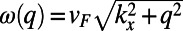
Here, we show how to design a specific gate electric potential to induce efficient electron backscattering through use of the optical-like character of graphene electron without introducing an external band gap engineering (which would degrade on current). We show that this can be accomplished using the saw-shaped gate electrode shown in Fig. 1A instead of a conventional bar-shaped gate electrode. The saw-shaped top gate electrode can be fabricated using electron beam lithography followed by atomic layer deposition of an insulating layer. The gate potential profile  is composed of a sawtooth part at the bottom and a bar-shaped blade back part connecting teeth to form a single piece of electrode (Fig. 1B). An explicit mathematical formulation of
  is given in Methods. Due to the symmetry in the graphene band, the hole dynamics of p-type channel can be also modulated using identical physics on the electron dynamics as for the n-type channel discussed hereafter.
Fig. 1.

(A) Schematic of sawtooth gate electrode used to implement the backscattering mechanism based on the optical analogy for graphene electrons for the design of a graphene field effect transistor. To maintain its high mobility, the graphene is sandwiched between h-BN sheets. The source/drain electrodes are located on top of the graphene sitting on a Si/SiO2 substrate. Then, the saw-shaped top gate electrode with an insulating layer (HfO2) is deposited. The top gate electrode is composed of sawtooth part and bar-shaped blade back part. (B) Top view of the simulation cell where periodic (or Bloch) boundary conditions are applied along the  direction. The sawtooth gate potential (transparent yellow-colored region) is characterized with a width
  , the lengths of the sawtooth
  , and the blade back part
  . The intervalley distance d linearly increases from 0 to
  while the
  coordinate changes from 0 to
  . The electron wave is excited from the bottom boundary, and then travels along the positive
  direction. (C) Fermi energy (EF) and gate potential (U0) are illustrated with the graphene energy band diagrams.
Results and Discussion
Graphene electron dynamics can be described in analogy to optical mode propagation (21–23). The gated region is an analog to waveguide cladding with an effective refractive index,  , where U0 is the potential height and
  is the incident electron energy (21). Here, each valley region between sawtooth elements can be regarded as a tapered waveguide. We note that single tapered optical waveguide using metamaterials has been proposed as a light-capturing device that effectively reduces the group velocity of guided electromagnetic waves (24, 25).
The sawtooth part of the gate potential can also be interpreted as a Kronig–Penney-type potential with a continuously varying barrier width. To understand the electron transport through this structure, it is useful to consider how eigenmodes of the Kronig–Penney potential are connected from source side ( ) to drain side (
 ). If an eigenstate connects smoothly across the gate potential, it serves as an electron-transmitting channel; otherwise, it serves as an electron-reflecting channel. In the optical analogy, these eigenmodes can be also viewed as guided modes in tapered waveguides. The longitudinal momentum eigenvalues (
 ) of these states are good quantum numbers defining the longitudinal electron propagation through the sawtooth potential, often used in optical waveguide analysis (26).
Interestingly, we found that the total number of electron-transmitting channels depends strongly on  , and eventually drops to 1 when
  regardless of the sawtooth pitch
  . From detailed analysis of the variation of eigenvalues (
 ) as a function of
  and
and  , we find that the connectivity of only the fundamental mode is independent of
  (thus always forming a transmitting channel), whereas that of the higher order modes can be regulated by appropriate choices of
  . For a sufficiently high gate potential of
  , all transmitting channels except the fundamental mode are eventually transformed into reflecting channels (a representative case is shown in Fig. 2A).
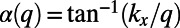
Fig. 2.

(A) The dependence of the eigenmodes formed in the valley regions (identified using the longitudinal momentum  ) on the intervalley width
  . This demonstrates how the connectivity of modes from
  to
to  can be transformed depending on the gate potential height
  [parameters here are chosen as
  (Upper) and
  (Lower),
  , and
, and  ]. When
  (Upper), five eigenmodes at the bottom end (
 ) are smoothly connected to the modes at the opposite top end (
 ), forming five electron-transmitting channels out of total nine modes. When
 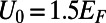 (Lower), only the fundamental mode is smoothly connected to the other end, while all higher order modes form electron-reflecting channels. This illustrates that the guided mode connectivity is modulated through
  . (B) Transmittance (
 ) of a normally incident electron propagating through the sawtooth potential system for
  ranging from 0 to 200 nm and
  ranging from 0 to 2.0
 (
( ,
,  ). The dashed lines show the conditions for the total internal reflections of an electron ray. Within this range of device size, low
  and high
  regimes are well separated depending on
  , which is explained in terms of (i) mode connectivity modulation and enhanced intermodal coupling due to nonadiabatic change of
  (from the wave nature of graphene electrons) also by (ii) the total internal reflection at the potential barrier interface (from the particle nature of the graphene electrons). The presence of well-defined low
  regime implies that the conductance modulation is possible using sawtooth gate potential.
This suggests that the higher population in excited modes can induce more backscattering of the graphene electron. An electron plane wave at normal incidence is entirely coupled to the fundamental eigenmode at the bottom end of the gate ( ) because their spatial profiles are identical. If the aspect ratio of a sawtooth,
  , is large enough to make the entire structure adiabatic, the electron would stay in the fundamental eigenmode while propagating along the structure and escape to the other end, resulting in a perfect transmission regardless of the gate voltage. However, if the aspect ratio is very small, a sawtooth geometry asymptotically resembles to a straight bar and thus the Klein tunneling recovers. Therefore, the aspect ratio of the sawtooth must be sufficiently small to ensure significant coupling between the eigenmodes, yet not too small to prevent the Klein tunneling.
Indeed, our numerical finite-difference time-domain simulations of graphene electron (GraFDTD) (21), solving graphene electronic dynamics within the assumption of ballistic and phase coherent transport, reveal that the electron tunneling can be substantially modulated by changing  , when
  and
and  are of similar order of magnitude, as shown in Fig. 2B. Electron ray tracing analysis adds more intuition on this system. The boundaries between high
  and low
  regions correspond well to the condition for total internal reflection, which is imposed by Snell’s law,
  , where
  is the angle of incidence of an electron ray on the sawtooth boundaries at mth reflection. The correspondence is apparent when
  is small so that each electron ray undergoes only one reflection before it escapes the structure, but becomes less vivid in the opposite regime where the system acts more like a wave-guiding structure. However, the ray tracing analysis does not provide a quantitative description. Particularly, even when the total internal reflection condition is satisfied,
  never vanishes but has a finite value due to the wave nature of the electron, which is directly related to the off current of the device.
The bar-shaped blade back part, required to structurally connect the saw teeth into a single gate structure, also helps suppress the transmittance. Because the bar-shaped potential can only transmit electrons at nearly normal incidence (5), the blade back part further reflects the nonnormal angle component of the transmitted electron through the sawtooth potential.
Thus, choice of proper device dimensions is vital to realize substantial backscattering. To illustrate this, consider an electron wave with  , yielding the Fermi wavelength
  , and
, and  . Transmittance through the sawtooth potential is minimized when the aspect ratio of a sawtooth,
  , independent of the overall structure size, as shown in Fig. S1. Therefore, we choose
  as 160 nm. As
  increases for given
  and
and  , the transmittance through the entire gate potential reaches its maximum when
  (Fig. S2). Therefore, we set
  .
.
Fig. 3A shows that the average transmittance  (defined in Methods) of the optimized saw-shaped gate under normal incidence exhibits a sharp on/off behavior depending on
  . We demonstrate a maximum of
  for 0 K and ∼80 for 300 K, which provides dramatic enhancements compared with the bar-shaped gate. The on/off ratio can be further enhanced by decreasing
 of the electron, either making the structure bigger or increasing
  (Fig. 3B). This can be understood in terms of the decreased wave nature of the electron (responsible for the nonzero transmittance) as the length scale of the structure becomes larger with respect to the electron wavelength. From snapshots of GraFDTD simulations such as in Fig. 3C when U0>EF (U0-dependent behavior is given in Fig. S3), we find that most of the incident electron plane wave undergoes a total internal reflection and escapes the structure (ray tracing point of view). In other words, the incident fundamental eigenmode is converted to the backward-propagating modes consisting of electron-reflecting channels due to the strong intermodal coupling inside the structure (waveguide point of view).
Fig. 3.

(A) The average transmittance ( ) of normally incident electrons is evaluated using finite-difference time domain simulations for the case
  ,
,  ,
,  , and
, and  while varying the top gate potential
  . We observe a well-defined on/off behavior, showing
 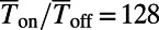 times enhanced compared with the bar-shaped gate for normally incident electrons (red circles). Considering the thermal broadening effect on the density of states at 300 K, the well-defined on/off behavior is still pertained with
 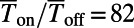 (blue squares). (B) Dependence of
  on
on  is shown. The other length scales,
  and
and  , are chosen to be
  and
and  , respectively; so that all of the length scales of the gate electrode are scaled. When the device is scaled up with respect to the electron wavelength (
 ), the on/off ratio increases linearly (the off current is measured at
  ). This implies that there is more room for optimization in between the device size (or the Fermi energy) and the on/off ratio. (C) Snapshots of an electron probability density profile when the device is at the off state illustrate the electron backscattering mechanism (to track its position, the packet is localized in the
  direction with the size of
 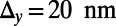 ). The device parameters are chosen as
  ,
,  ,
,  ,
,  , and
, and  . The electron is introduced from the bottom boundary at
  . The freestanding electron travels, and then it is coupled to the guided modes in the valley region of the gate potential (
 ). It further propagates along the
  direction, and the electron wave undergoes a total internal reflection. Most parts of the electron wave are reflected back while small amount transmits the potential barrier induced by the top gate (t = 128–196 fs).
SI Text, Robustness Analysis reports an extensive investigation of the robustness of the proposed gate modulation, by taking into account realistic experimental conditions (Figs. S4–S7). We find that breaking the perfect periodicity of the sawtooth pitch up to 10% changes the  by only <5% (Fig. S4). We also considered the effect of potential blurring due to the finite thickness of the gate oxide and confirmed that the proposed switching mechanism is robust enough to maintain high on/off ratio (
 ) when the thickness of the oxide layer (HfO2) is 2 nm (Fig. S5). Further theoretical investigation using the nonequilibrium Green’s function formalism combined with tight binding or large-scale density functional theory calculation would be useful to take into account the effect of finite drain source bias and high-temperature dephasing effects (27, 28).
For obliquely incident electrons, we find that the highly suppressed transmission through the gate potential is still preserved for incidence angles in the range  even at room temperature. By applying Bloch boundary conditions along the transverse direction, we calculate
  for
for  (Fig. 4). This shows that the saw-shaped gate potential exhibits large electron backscattering over a substantial angular range near 0°, which is the dominant incident angle for electron current flows driven by the electric field applied from the source to the drain electrode (29).
Fig. 4.

Dependence of the off-state transmittance ( ; measured at
  ) on the incident angle (
 ) for the sawtooth gate potential with
 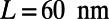 ,
,  , and
, and  at zero temperature (red circles) and at room temperature (blue squares). For comparison, same plots for the bar-shaped gate potential with the gate length of
 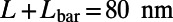 are shown for 0 K (red solid) and 300 K (blue dashed). The sawtooth gate potential shows highly suppressed transmission near normal incidence
  even at room temperature, whereas the bar-shaped gate potential shows considerably high transmittance for the same range of
  . Note that the electrons with smaller incident angle contribute more on the total current flow compared with those that have larger
  . Recognizing that the bar-shaped gate potential exhibit little transmittance for large angle of incidence
  , it may further enhance the size of the
  window for low
  by placing a bar-shaped gate and a sawtooth gate in series (Inset).
Furthermore, we propose a dual gate system composed of a saw-shaped gate electrode and a bar-shaped gate electrode in series could be used to suppress electron transmittance by reflecting both normally incident and nonnormally incident electrons in series (Fig. 4, Inset). It may be possible to further reduce the transmission by configuring sawtooth shapes other than linear to engineer the mode conversion more effectively. Also, the simultaneous modulation of the back-gate voltage (along with the top-gate voltage) would allow us to further control the carrier density of the channel of the device, leading to a further increase in the on/off ratio. Because our proposed mechanism for graphene field effect transistors is quite robust, we anticipate that it can be experimentally realized. Moreover, our current theoretical study opens a possibility for graphene-based device optimization by engineering the gate geometry.
Methods
GraFDTD Simulations.
To solve the time-dependent Dirac equation,  , on a two-dimensional spatial grid, we discretize the time domain using the velocity Verlet algorithm, whereas the spatial derivatives are treated by using finite-difference methods. The details of our simulation method were fully described previously (21).
Electric Potential Profile.
A periodic potential 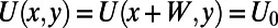 is applied, where
  and
and  (sawtooth part) or
 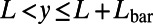 (blade back part).
  everywhere else.
Boundary Conditions.
Because the potential profile has translation invariance along the  direction with the periodicity
  , the wave function will have the form of a Bloch wave,
  , where
  is the angle of incidence. Therefore, we impose a Bloch boundary condition on the left (
 ) and the right (
 ) boundaries of our simulation cell,
  . An electron wave function is excited from the bottom boundary by the second-order approximation of
  , where
  ,
,  ,
,  , and
, and  is the normalization factor. Unless otherwise specified, the width of the
  directional Gaussian packet is taken to be
 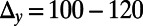 nm.
nm.
Transmittance.
We determine the transmission probability  for an electron with energy
  by integrating the probability density (|Ψ|2) over the drain region (
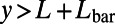 ). We define the average transmittance
 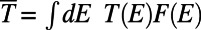 , where
 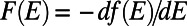 is the energy distribution of electrons participating in conduction (30).
  is the Fermi distribution function. Note that, at zero temperature,
 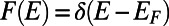 , resulting in
 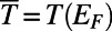 . Unless otherwise specified, we assume zero temperature.
Supplementary Material
Acknowledgments
This work was supported by Department of Energy Light-Material Interactions in Energy Conversion–Energy Frontier Research Center Grant DE-SC0001293 (to M.S.J. and H.A.A.), the National Science Foundation (CMMI-1120890, to W.A.G.), and the Functional Engineered Nano Architectonics via the Microelectronics Advanced Research Corporation with Prime Award 2009-NT-2048 at University of California, Los Angeles (to W.A.G.). H.K. and W.A.G. also acknowledge support from the World Class University programs through National Research Foundation (NRF) of Korea funded by Ministry of Education, Science and Technology (MEST) Grant R31-2008-000-10055-0. H.K. also is grateful for the support of the Nanomaterial Technology Development Program through the NRF of Korea funded by MEST Grant 2012M3A7B4049807. Y.-W.S. was in part supported by MEST (Grant QMMRC R11-2008-053-01002-0 and Center for Advanced Soft Electronics 2011-0031640).
Footnotes
The authors declare no conflict of interest.
This article contains supporting information online at www.pnas.org/lookup/suppl/doi:10.1073/pnas.1305416110/-/DCSupplemental.
References
- 1.Castro Neto AH, Guinea F, Peres NMR, Novoselov KS, Geim AK. The electronic properties of graphene. Rev Mod Phys. 2009;81(1):109–162. [Google Scholar]
- 2.Young AF, Kim P. Quantum interference and Klein tunnelling in graphene heterojunctions. Nat Phys. 2009;5(3):222–226. [Google Scholar]
- 3.Stander N, Huard B, Goldhaber-Gordon D. Evidence for Klein tunneling in graphene p-n junctions. Phys Rev Lett. 2009;102(2):026807. doi: 10.1103/PhysRevLett.102.026807. [DOI] [PubMed] [Google Scholar]
- 4.Schwierz F. Graphene transistors. Nat Nanotechnol. 2010;5(7):487–496. doi: 10.1038/nnano.2010.89. [DOI] [PubMed] [Google Scholar]
- 5.Katsnelson MI, Novoselov KS, Geim AK. Chiral tunnelling and the Klein paradox in graphene. Nat Phys. 2006;2(9):620–625. [Google Scholar]
- 6.Avouris P. Graphene: Electronic and photonic properties and devices. Nano Lett. 2010;10(11):4285–4294. doi: 10.1021/nl102824h. [DOI] [PubMed] [Google Scholar]
- 7.Meric I, et al. Current saturation in zero-bandgap, top-gated graphene field-effect transistors. Nat Nanotechnol. 2008;3(11):654–659. doi: 10.1038/nnano.2008.268. [DOI] [PubMed] [Google Scholar]
- 8.Son YW, Cohen ML, Louie SG. Energy gaps in graphene nanoribbons. Phys Rev Lett. 2006;97(21):216803. doi: 10.1103/PhysRevLett.97.216803. [DOI] [PubMed] [Google Scholar]
- 9.Son YW, Cohen ML, Louie SG. Half-metallic graphene nanoribbons. Nature. 2006;444(7117):347–349. doi: 10.1038/nature05180. [DOI] [PubMed] [Google Scholar]
- 10.Han MY, Ozyilmaz B, Zhang YB, Kim P. Energy band-gap engineering of graphene nanoribbons. Phys Rev Lett. 2007;98(20):206805. doi: 10.1103/PhysRevLett.98.206805. [DOI] [PubMed] [Google Scholar]
- 11.Chen ZH, Lin YM, Rooks MJ, Avouris P. Graphene nano-ribbon electronics. Physica E. 2007;40(2):228–232. [Google Scholar]
- 12.Lu YH, et al. Effects of edge passivation by hydrogen on electronic structure of armchair graphene nanoribbon and band gap engineering. Appl Phys Lett. 2009;94(12):122111. [Google Scholar]
- 13.Balog R, et al. Bandgap opening in graphene induced by patterned hydrogen adsorption. Nat Mater. 2010;9(4):315–319. doi: 10.1038/nmat2710. [DOI] [PubMed] [Google Scholar]
- 14.Elias DC, et al. Control of graphene’s properties by reversible hydrogenation: Evidence for graphane. Science. 2009;323(5914):610–613. doi: 10.1126/science.1167130. [DOI] [PubMed] [Google Scholar]
- 15.De Martino A, Dell’Anna L, Egger R. Magnetic confinement of massless Dirac fermions in graphene. Phys Rev Lett. 2007;98(6):066802. doi: 10.1103/PhysRevLett.98.066802. [DOI] [PubMed] [Google Scholar]
- 16.Bai JW, Zhong X, Jiang S, Huang Y, Duan XF. Graphene nanomesh. Nat Nanotechnol. 2010;5(3):190–194. doi: 10.1038/nnano.2010.8. [DOI] [PMC free article] [PubMed] [Google Scholar]
- 17.Bolotin KI, et al. Ultrahigh electron mobility in suspended graphene. Solid State Commun. 2008;146(9–10):351–355. [Google Scholar]
- 18.Mayorov AS, et al. Micrometer-scale ballistic transport in encapsulated graphene at room temperature. Nano Lett. 2011;11(6):2396–2399. doi: 10.1021/nl200758b. [DOI] [PubMed] [Google Scholar]
- 19.Murali R, Yang YX, Brenner K, Beck T, Meindl JD. Breakdown current density of graphene nanoribbons. Appl Phys Lett. 2009;94(24):243114. [Google Scholar]
- 20.Du X, Skachko I, Barker A, Andrei EY. Approaching ballistic transport in suspended graphene. Nat Nanotechnol. 2008;3(8):491–495. doi: 10.1038/nnano.2008.199. [DOI] [PubMed] [Google Scholar]
- 21.Jang MS, Kim H, Atwater HA, Goddard WA. Time dependent behavior of a localized electron at a heterojunction boundary of graphene. Appl Phys Lett. 2010;97(4):043504. [Google Scholar]
- 22.Park CH, Son YW, Yang L, Cohen ML, Louie SG. Electron beam supercollimation in graphene superlattices. Nano Lett. 2008;8(9):2920–2924. doi: 10.1021/nl801752r. [DOI] [PubMed] [Google Scholar]
- 23.Vakil A, Engheta N. Transformation optics using graphene. Science. 2011;332(6035):1291–1294. doi: 10.1126/science.1202691. [DOI] [PubMed] [Google Scholar]
- 24.Tsakmakidis KL, Boardman AD, Hess O. “Trapped rainbow” storage of light in metamaterials. Nature. 2007;450(7168):397–401. doi: 10.1038/nature06285. [DOI] [PubMed] [Google Scholar]
- 25.Jang MS, Atwater H. Plasmonic rainbow trapping structures for light localization and spectrum splitting. Phys Rev Lett. 2011;107(20):207401. doi: 10.1103/PhysRevLett.107.207401. [DOI] [PubMed] [Google Scholar]
- 26.Snyder AW, Love JD. Optical Waveguide Theory. London: Chapman and Hall; 1983. [Google Scholar]
- 27.Golizadeh-Mojarad R, Datta S. Nonequilibrium Green’s function based models for dephasing in quantum transport. Phys Rev B. 2007;75(8):081301. [Google Scholar]
- 28.Low T, Appenzeller J. Electronic transport properties of a tilted graphene p-n junction. Phys Rev B. 2009;80(15):155406. [Google Scholar]
- 29.Sutar S, et al. Angle-dependent carrier transmission in graphene p-n junctions. Nano Lett. 2012;12(9):4460–4464. doi: 10.1021/nl3011897. [DOI] [PubMed] [Google Scholar]
- 30.Datta S. Electronic Transport in Mesoscopic Systems. Cambridge, UK: Cambridge Univ Press; 1995. [Google Scholar]
Associated Data
This section collects any data citations, data availability statements, or supplementary materials included in this article.