Abstract
Hetero interfaces between metal-oxides display pronounced phenomena such as semiconductor-metal transitions, magnetoresistance, the quantum hall effect and superconductivity. Similar effects at compositionally homogeneous interfaces including ferroic domain walls are expected. Unlike hetero interfaces, domain walls can be created, displaced, annihilated and recreated inside a functioning device. Theory predicts the existence of 'strongly' charged domain walls that break polarization continuity, but are stable and conduct steadily through a quasi-two-dimensional electron gas. Here we show this phenomenon experimentally in charged domain walls of the prototypical ferroelectric BaTiO3. Their steady metallic-type conductivity, 109 times that of the parent matrix, evidence the presence of stable degenerate electron gas, thus adding mobility to functional interfaces.
 Although ferroelectrics are generally insulating, their domain walls can show electrical conductivity. Here Sluka et al. observe a highly conducting free-electron gas at charged domain walls in ferroelectric BaTiO3.
Solid interfaces between two distinct materials or material states are quasi-two-dimensional objects, which display uniquely distorted electronic structures and ionic displacements. Properties of such interfaces may, therefore, be entirely different from those of the parent materials. Indeed, technologically enticing phenomena were found at hetero interfaces between metal-oxides2,3,4,5,6,7,8 and in compositionally homogeneous interfaces such as ferroic domain walls9,10,11,12,13,14,15,16,17,18. The anomalous properties at domain walls in ferroics are especially attractive for their variability. Domain walls can change positions, shapes and thereby also intrinsic properties in a controlled way so that they could be utilized inside a ready device19. So far, the reported anomalies at ferroic domain walls are mostly weak in magnitude. However, drastic property deviations are theoretically predicted at specific types of charged domain walls in ferroelectrics20,21,22. These domain walls represent a fascinating unexplored arena.
Ferroelectrics domain walls are nanometric-scale transitions between two ferroelectric domain states, which differ in the orientation of a switchable spontaneous polarization. As secondary order parameters like spontaneous strain are usually induced by the polarization, ferroelectrics are mostly also improper ferroelastics. Therefore, as domain walls are mobile, their geometry is naturally forced towards equilibrium with electrostatic neutrality between adjacent ferroelectric domains and towards minimal strain mismatch between ferroelastic domains. Whenever this equilibrium is slightly perturbed, the domain walls become weakly charged due to polarization divergence. This occurs during ordinary processes like domain switching or domain-wall bending by external forces16,23,18. Such weakly charged domain walls showed transient enhanced conductivity, 103 times that of the bulk, during switching in Pb(Zr0.2Ti0.8)O3 thin films16 and steady enhanced conductivity under illumination with above-bangap-energy photons in LiNbO3 cystals18. These domain walls shown signs of metallic-like behaviour, but they are impractically unstable16 or must be pinned by defects18.
An exotic family of domain walls was found in improper ferroelectrics YMnO3 (24) and ErMnO3 (17). These materials naturally lock ferroelectric domain walls with a wide range of orientations including stable charged configurations. Tail-to-tail domain walls in ErMnO3 showed some three times the conductivity of the semiconducting bulk while head-to-head domain walls displayed a conductivity drop17. However, unlike in ordinary ferroelectrics, the spontaneous polarization in manganese oxides is a secondary order parameter induced by a structural phase transition (PT). This mechanism drives the polarization with substantially different thermodynamic forces than in ordinary ferroelectrics25. Thus, properties of charged domain walls in proper and improper ferroelectrics cannot be generally linked. For example, manganese oxides, unlike ordinary ferroelectrics, cause the unusual topological locking of the polar and antiphase boundaries and do not necessarily require compensation of charged domain walls26.
In proper ferroelectrics, the existence of such ‘strongly' charged domain walls (sCDW) depends vitally upon almost perfect compensation of the polarization charge. The compensation can be provided by mobile defects, which also stabilize the domain walls, but in this case, the domain-wall properties are not expected to display exceptional new features27,18. In contrast, theory predicts20,21,22 the existence of qualitatively different, electron- and hole-compensated sCDW in ordinary wide-bandgap ferroelectrics. These sCDW can be stable while completely breaking polarization continuity. They form head-to-head and tail-to-tail polarization divergences as illustrated in Fig. 1 leading to high concentrations of polarization charge. Formation of this bound charge is simultaneously counterbalanced by two stabilizing factors: (i) free-carrier compensation of the polarization charge at the walls and (ii) clamping of two ferroelastic states. Thus, sCDW might be flat and mobile while covered with free carriers.
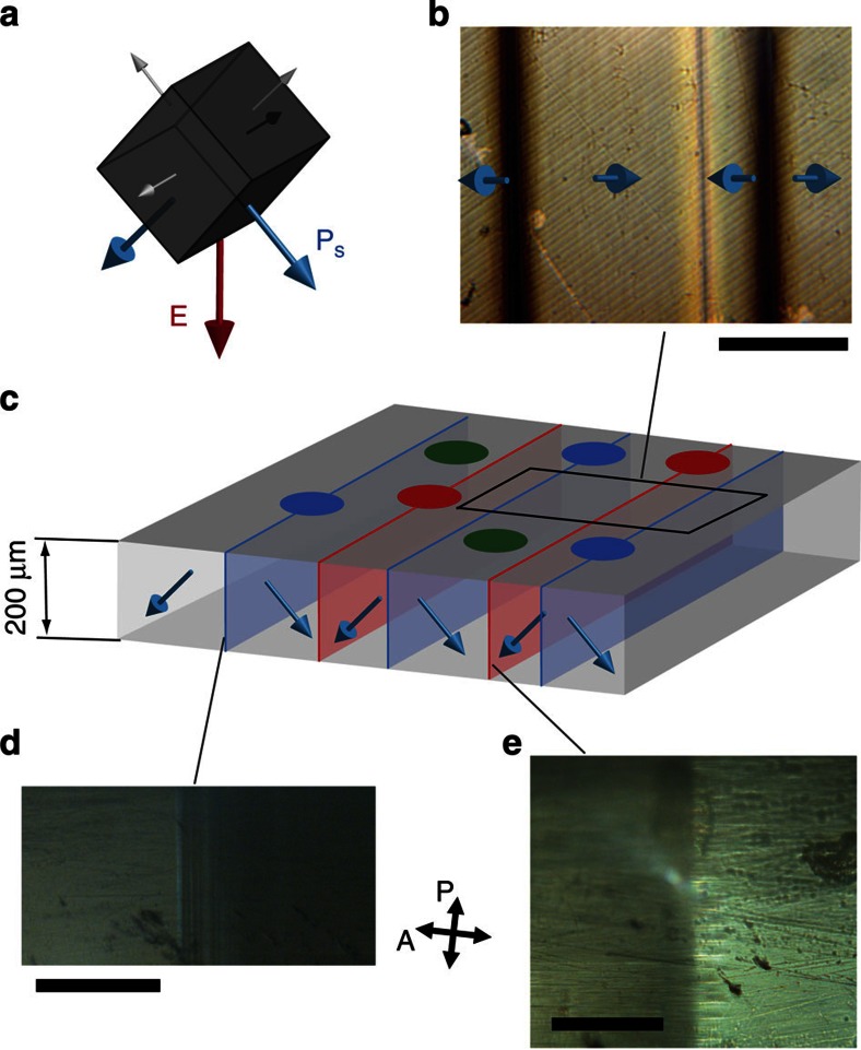
Figure 1. Charged domain walls in tetragonal BaTiO3.
(a) Poling of the crystal in a [110]c-like direction (red arrow) allows two equally preferred ferroelectric domain states (blue arrows) out of the six permitted (blue and grey arrows). When the frustrated poling is applied during a slow paraelectric-ferroelectric PT, tail-to-tail (b–d) and head-to-head (b,c,e) domain walls are formed. (b) Top view micrograph with light transmitted through the sample in the [110]c direction. Scale bar, 200 μm. (c) Out-of-scale cartoon illustrates a 200 μm thick (110)c sample with 5 × 5 mm2 top surface covered with 200 μm diameter and 400 μm period electrodes. The domain walls are irregularly distributed with period from 100 to 300 μm. (d,e) Side view micrographs with light transmitted in the [001]c direction show the tail-to-tail domain walls (scale bar, 100 μm) and head-to-head domain wall (scale bar, 25 μm), respectively. P denotes polarization of incident light and A polarization filter on transmitted light.
Why should these sCDW be technologically interesting? The free-charge compensation at sCDW must be almost complete in order to reduce the depolarizing field that would otherwise prohibit their formation or kill ferroelectricity20,21. For realistic parameters of ferroelectric perovskites (unless these are heavily doped), such compensation cannot be provided with the typical free-carrier concentration in these materials. Most of the screening charge originates from electron transfer across the forbidden energy gap or an external charge injection. Theoretical calculations predict that the charge compensation at stable sCDW in ordinary ferroelectrics results in the formation of degenerate quasi-two-dimensional electron gas (q2DEG) with metallic free-carrier concentration20,21,22. This high concentration might result in a pronounced steady metallic-type conductivity of sCDW and other properties linked to an electron gas confinement in their energy well.
While the intrinsic properties of neutral and weakly charged domain walls are being rapidly revealed11,12,13,14,15,16,18,28, sCDW remain poorly understood, especially on the experimental level. sCDW are rarely formed naturally due to their high energy21 and methods of their artificial formation have been seldom investigated18,29,30. Sporadic naturally formed sCDW have been detected in unpoled thin films31,32 and indirectly identified in bulk crystals29,30, but their electronic properties have hardly ever been reported.
Here we show experimental evidence for the q2DEG at stable 90° sCDW of the prototypical wide-bandgap proper ferroelectric BaTiO3. The sCDW show giant steady metallic-type conductivity, 109 times that of the BaTiO3 bulk. We support the experimental findings by theory and phase field simulations, which explain the properties of sCDW and the role of sCDW-electrode junctions.
Results
Experimental
The sCDW are created by so-called frustrated poling30. An electric field, E, is applied to a (110)c plate of tetragonal BaTiO3 in a [110]c-like direction. This leads to two equally preferred ferroelectric-ferroelastic domain states, Fig. 1a, which can be separated either by (110)c neutral domain walls or (10)c sCDW. The theoretical energy density of sCDW is significantly larger than that of the neutral domain walls21, but their total energy in a thin plate sample can be smaller due to their smaller total surface. The sCDW are stabilized by elastic compatibility of adjacent ferroelastic states, therefore, their density can be controlled by favourable poling history and boundary conditions30.
Frustrated poling of BaTiO3 samples during slow cooling over the paraelectric-ferroelectric PT led to the formation of (10)c planar sCDW, Figs 1b–e. The full Pt electrodes used for the poling were then replaced with circular Pt electrodes of 200 μm diameter and 400 μm period on the side with negative polarization charge, Fig. 1c. This configuration resulted in similar fractions of electrodes touching head-to-head, tail-to-tail or no domain walls. By measuring charge transfer between the bottom and individual upper electrodes, one can clearly relate changes in the conductances to the presence of sCDW.
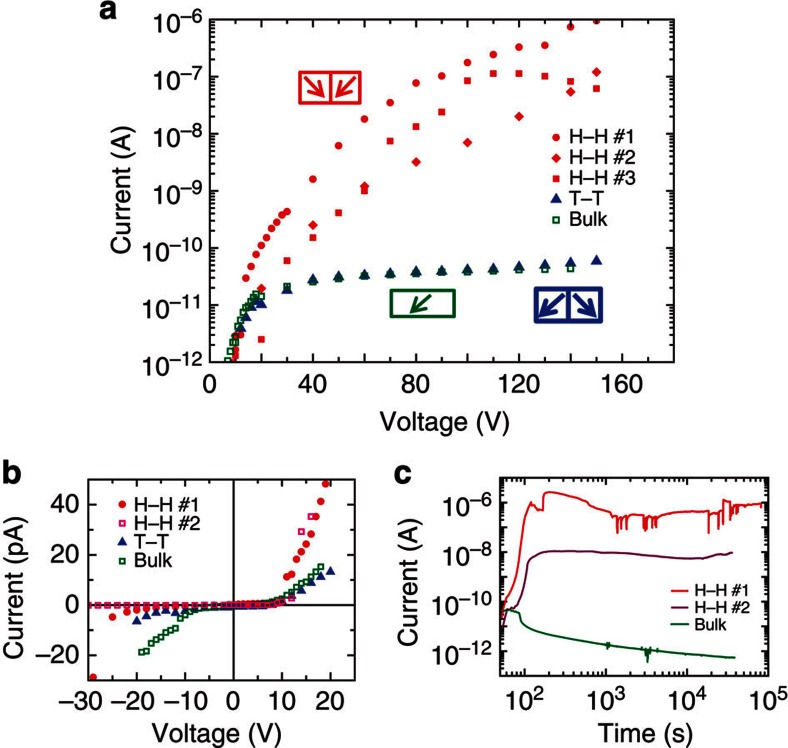
The conduction between electrodes connected by tail-to-tail sCDW was almost identical to the conduction through the bulk. The conduction between electrodes touching head-to-head sCDW was reproducibly and steadily (for >120 h) 104–106 times higher, Fig. 2. We confirmed this exclusive relation between head-to-head sCDW and giant conductivity by testing 30 different spots on ten different walls and on the bulk.
Figure 2. Conduction through charged domain walls in BaTiO3.
(a) Semilogarithmic-scale room-temperature I–V characteristics showing up to 105 times higher conduction through electrodes touching head-to-head (H–H) charged domain walls compared with the bulk and tail-to-tail (T–T) domain walls. (b) Linear-scale I–V curve showing ~8 V conduction threshold indicating barriers between electrodes and ferroelectric. Each datapoint in (a,b) is acquired 1 min after step change of applied voltage, hence, the values include transient currents. The difference between H–H current and bulk is, therefore, underestimated here. The steady current through the bulk (at V=100 V after>660 min) is 6 × 10⁻¹³ A, while H–H wall reaches steady 10−6 A, shown in c. The current increase during first 200 s in c corresponds to slowly applied voltage. Attributing the current difference between H–H domain wall and the bulk to domain wall itself, its intrinsic conductivity is 108−1010 times that of the bulk.
Figures 2a show room-temperature I–V curves of the bulk and the cases when a single head-to-head or tail-to-tail domain wall is present between the tested electrodes. One can see, in Figs 2b conduction threshold at ~8 V indicating non-ohmic contact between the electrodes and the ferroelectric. Each datapoint in Figs 2a is acquired 1 min after step change of applied voltage, hence, the values include transient currents seen on Fig. 2c. The steady difference between conductance measured with and without the head-to-head sCDW is more than six orders of magnitude (at V=100 V after >660 min), Fig. 2c. Assuming the thickness of sCDW is 10–100 nm 22, its intrinsic conductivity is 108–1010 times higher than the conductivity of the bulk.
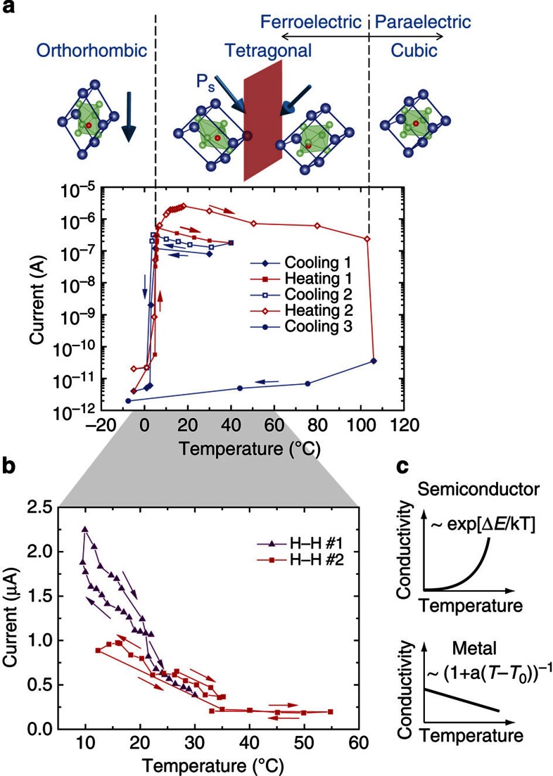
Strong evidence that the head-to-head sCDW are the objects providing free carriers for the measured current is seen at the tetragonal-orthorhombic and ferroelectric-paraelectric PTs, Fig. 3a. The 90° sCDW formed in tetragonal BaTiO3 cannot exist in other phases due to their different symmetries as illustrated in the cartoon in Fig. 3a. One can see that the electric current drops and rises by four to six orders of magnitude when cooling and heating, respectively, across the tetragonal-orthorhombic phase boundary at ~3 °C. When crossing the ferroelectric-paraelectric PT at ~110 °C, Fig. 3a, the current drops to values typical for the bulk and remains such after cooling down to the tetragonal and orthorhombic phases. The sCDW under the measured electrodes are annihilated during the PT. All in all, the giant conductance was measured conclusively only when a head-to-head sCDW was present between the electrodes.
Figure 3. Switching metallic-type properties of charged domain walls.
(a) Current–temperature dependence shows switching of the metallic-type conductivity when a 90° head-to-head (H–H) charged domain wall is created and annihilated at PTs. The domain walls formed in tetragonal BaTiO3 cannot exist in the orthorhombic and paraelectric phases as illustrated in the cartoon. The charged domain wall is annihilated at both transitions from the tetragonal phase. The annihilation at the transition to the paraelectric phase is permanent in this case. The conductivity characteristic shows change from metallic-type temperature dependence and magnitude to thermally activated conduction typical for wide-bandgap semiconductor bulk BaTiO3. (b) Linear-scale current–temperature dependence showing pronounced positive temperature coefficient indicating thermally non-activated (that is, metallic-type) conduction at domain walls as illustrated in c.
The current–temperature characteristics, Fig. 3, show that the conduction through head-to-head sCDW is not dominated by thermal activation like in semiconductors or ionic conductors, that is, like in the BaTiO3 bulk, but has the opposite, metallic-type trend with positive temperature coefficient, Figs 3b. Clearly the temperature dependence of sCDW conductivity is influenced also by temperature dependence of spontaneous polarization and domain-wall width, but these factors would be minor relative to the exponential character of thermally activated conduction if the latter were the dominant mechanism.
Simulation
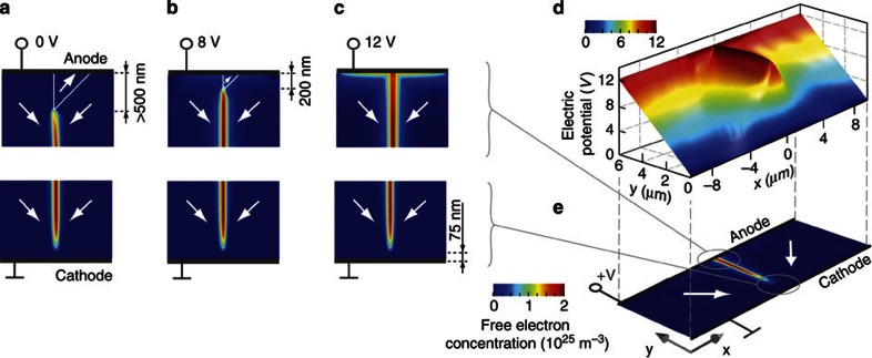
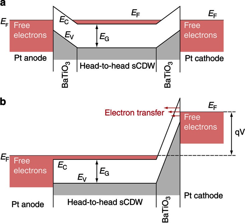
Why is this giant sCDW conduction not observed regularly? Obviously, the rare natural occurrence of sCDW due to their high-energy density21 makes them practically unavailable unless they are prepared artificially. However, additional principal factors hinder the experimental access to the free-carriers at sCDW. At low voltages, the q2DEG at head-to-head sCDW is separated from electrodes by an insulating wedge domain at the anode and an insulating gap at the cathode as seen in phase field simulation results in Fig. 4a (method in Supplementary Note 1, parameters in Supplementary Table S1) and as illustrated on the band diagram of the cross-section through a head-to-head sCDW in Fig. 5a. The calculation corresponds to zero difference between work-functions of the electrode and BaTiO3, but it is qualitatively valid for the vast majority of conductors including Pt used here. The insulating regions are formed due to flattening of electric potential profile by the equipotential electrodes. The mechanism is as follows: compensation of sCDW requires dramatic band bending when the bottom of the conduction band drops below the Fermi level at head-to-head sCDW (Fig. 5) and the top of the valence band rises over the Fermi level at tail-to-tail sCDW (Supplementary Fig. S1). Otherwise, there would be no available energy states, which could be occupied by compensating free carriers. Recurring sCDW form built-in triangle-wave potential profiles (Supplementary Figs S1 and S2) with amplitude equal to the BaTiO3 bandgap22. This cannot be satisfied by the electrodes which dictate value and the (flat) profile of the potential, thus, the potential difference between sCDW and electrodes forms a transition region that is insulating and exposed to high electric field. This field has a depolarizing direction between anode and head-to-head sCDW, which nucleates the wedge-like domain (Fig. 4 and Supplementary Fig. S3) or other anti-polar domain structures22. The electric field in the poling direction is applied across the insulating gap between head-to-head sCDW and the cathode as shown in Figs 4 and 5 and Supplementary Figs S1 and S4. This situation is inverted at tail-to-tail sCDW, that is, the wedge domain is at the cathode and the insulating gap at the anode22 (Supplementary Fig. S1). Both sCDW are, therefore, disconnected from the electrodes.
Figure 4. Connecting a charged domain wall and electrodes by an applied voltage.
(a–c) Colour-scale map of the phase field calculated free-electron concentration at a head-to-head domain wall when an electric potential is being applied. The wedge-like domain disconnects the free-electron gas from the anode when the potential difference is below 8 V. The free-electron gas is permanently disconnected from the cathode. (d) Colour-scaled landscape of electric potential in the vicinity of the domain wall when 12 V is applied. The charged domain wall is at equipotential with the anode. (e) Illustration of the polarization (arrows) and free-charge (color-scale) distribution under the applied 12 V.
Figure 5. Schematic of the band structure at head-to-head domain wall.
Conduction band, EC, drops below the Fermi level, EF, at head-to-head strongly charged domain walls (sCDW). At 0 V, (a), sCDW is separated from both electrodes by dielectric regions, which are exposed to high electric fields (given by the potential slope). The electric field at the anode has a depolarizing direction and nucleates an anti-polar domain as seen in Fig 4a. At the cathode, the field has a poling direction. (b) Under an applied potential difference, the barrier at the anode is annihilated and the electron gas at sCDW connects the electrode. The dielectric barrier at the cathode is exposed to the applied potential difference. Theory allows high Fowler–Nordheim tunnelling current through the barrier with realistic parameters. Additional mechanisms, especially those related to oxygen vacancy accumulation, may contribute.
In most cases, the conducting path through the q2DEG at head-to-head sCDW can be established only when the wedge domain at the anode, Fig. 4a, is annihilated by the local electric field and the insulating gap at the cathode is penetrated by electron tunnelling (Fig. 5b), hence I–V curves should exhibit threshold characteristics such as those in Fig. 2b. The wedge domain at the anode is reduced upon increase of applied voltage V between the electrodes and annihilated when V >8 V. Note that the threshold value in real system should be history and case dependent as is domain nucleation. We have observed such unsettled conduction thresholds at fresh sCDW.
The simulation results in Figs 4c–e, show the situation where the electric potential (V=12 V) already connects the q2DEG with the anode (schematics in Fig. 5b). On the other hand, a permanent insulating gap remains between the q2DEG and the cathode, Fig. 4. However, when the q2DEG is connected to the anode, Figs 4c–e and Fig. 5b, the applied voltage drops entirely over the junction at the cathode, exposing the insulating gap to giant electric fields, theoretically up to ~105 V mm−1 when 10 V is applied. A lower bound conductivity estimate, given by sole Fowler–Nordheim tunnelling through the insulating gap (Supplementary Note 2) reaches the experimentally measured values, that is, ~10−6 A at 100 V, when the barrier height is up to 2 V and the gap thickness is up to 90 nm, thus, providing sufficient current for realistic barrier parameters (results summarized in Supplementary Figs S5–S7).
Clearly this tunnelling can be further enhanced by defect-assisted charge transfer mechanisms33 and by additional reduction of the barrier thickness due to accumulation of usually present oxygen vacancies, Vö, near to the Pt electrodes34 (Supplementary Fig. S4). This might happen especially under poling fields, which drive the positively charged Vö towards the cathode. The accumulated Vö narrow the barrier34 and provide empty energy levels ~0.4 eV below the conduction band of BaTiO3 for additional trap-assisted tunnelling, which might result in significantly higher charge transport than the sole Fowler–Nordheim tunnelling. As the tunnelling current has a small negative temperature coefficient, we associate the measured current–temperature dependence in Fig. 3 to the sCDW themselves.
One can see in Fig. 2a, that tail-to-tail sCDW do not exhibit apparently higher conductivity compared with the bulk even though, in defect-free material, they should form a conductive quasi-two-dimensional hole gas22 (Supplementary Fig. S1). The reason for low conductivity of tail-to-tail sCDW is not positively identified, but according to our simulations (Supplementary Note 1), free-carrier concentration at these walls can be suppressed by accumulation of Vö. A small initial concentration of Vö (1018 m−3) is sufficient to accumulate at tail-to-tail sCDW and substitute screening holes (Supplementary Fig. S2). The calculated accumulation time is <10 h, which is short compared with the time between sCDW formation and their characterization in our experiments. On the other hand, Vö deplete from head-to-head sCDW leaving the q2DEG intact and available for conduction (Supplementary Figs S2 and S4). All in all, accumulation of Vö in theory suppresses conduction through tail-to-tail sCDW while it enhances the electron transfer through the barrier between the q2DEG at head-to-head sCDW and the Pt cathode.
Note, that insulating barriers between electrodes and either tail-to-tail or head-to-head sCDW in defect-free material would be theoretically reduced to zero and form ohmic contacts when the electrode material had a work-function, respectively, smaller or bigger than BaTiO3 by more than half of the BaTiO3 bandgap, that is, by more than ~1.5 V. Most conductors have their work-functions below this limit. Additionally, the work-function, especially in metal-oxides is an extremely sensitive measure of the surface state, which is strongly dependent on surface preparation and the measurement technique, making it hard to control in experiments. However, according to the text-book values, Pt with its exceptionally high work-function ~5.7 V which is 1.5 V more than ~4.2 V of BaTiO3 should support spontaneous formation of tail-to-tail sCDW and create their ohmic contact. In reality, we observed neither spontaneous sCDW formation nor their ohmic contact with electrodes, which is not surprising when work-function sensitivity and drift of Vö is considered.
Discussion
In summary, our experiment showed that 90° head-to-head sCDW in the classical ferroelectric BaTiO3 are stable and exhibit qualitatively pronounced metallic behaviour with a steady conductivity ~109 times the bulk DC conductivity of BaTiO3. Our analysis, supported with phase field simulations, relate the observation to the presence of a degenerate q2DEG, which is held in a potential well formed by the polarization charge.
In contrast to the phenomenon observed in improper ferroelectrics17, where 101 times enhanced conductivity was observed at tail-to-tail domain walls, the almost perfect compensation of polarization charge by degenerate free carriers (in the absence of defect compensation) is indispensable for the existence of sCDW. While the proper ferroelectricity in typical perovskites would be suppressed by the depolarizing field that is created in the absence of the screening charge at charged domain walls, the improper ferroelectricity would not be suppressed in such a case as it can lower its energy by reduction of polarization. Thus, sCDW in pure ordinary ferroelectrics must exhibit giant conductivity via degenerate free carriers by default, while the conductivity of locked charged domain walls in improper ferroelectrics is case dependent.
The concept shown above could be implemented in other proper ferroelectrics. Yet, writing stable charged domain walls in the classical ferroelectric insulator BaTiO3 as shown here is of an extra appeal as, unlike most of the applied ferroelectrics, this material is lead-free and composed of abundant elements. In addition, charged domain walls in BaTiO3 are predicted to be exceptionally thick22 making it a suitable material for fundamental studies. Additional intriguing properties of the q2DEG are likely to exist also in sCDW. Emerging oxide electronics that use the q2DEG and other hetero interfacial properties8,35, might also incorporate the new phenomena described here, where q2DEG could be electrically displaced, erased and recreated inside ready devices, ultimately adding interface mobility to future electronic elements.
Methods
Sample preparation
Undoped (110)c plates of BaTiO3 were cut into 5 × 5 × 0.5 mm3 pieces and lapped to 200 μm thickness with diamond films of roughness from 15 to 0.1 μm. The samples, cleaned with acetone and isopropanol, were sputtered with 12 nm thick Pt electrodes on [110]c surfaces. Samples were heated while observed with a polarization microscope in transmitted light. Slow (0.2 °C/min) heating from 100 °C while switching on and off 350 V (~1 switch min−1) allows optical identification of (i) zero field and (ii) the field-induced PTs. After heating up to 0.7 °C above the field-induced PT, the samples were slowly (0.1 °C min−1), without electric field, cooled up to ~0.1 °C below the field-induced PT temperature. Then, 350 V was rapidly applied inducing the PT and a periodic structure with (10)c planar sCDW. This process is strongly sensitive on poling conditions, often creating walls, which do not pass through the whole sample or form zig-zag-like neutral walls. The Pt electrode on the anode was removed by 1 μm diamond paste and replaced with sputtered 150 nm thick, 200 μm diameter circular Pt electrodes with 400 μm period.
Conductivity measurement
At room-temperature, I–V characteristics between 30 different top electrodes and the bottom electrode were measured with a Keithley 6517A electrometer. Measurement was conducted in a dark and electrically shielded box. Voltage was applied in steps (seen in Figs 2a) and current was averaged between 60 and 70 s later. The current–temperature measurement was done in a DELTA 9023 chamber. Temperature was changed in steps (Fig. 3), while voltage was kept constant at 100 V. Current was acquired when it fluctuated <10% for more than 10 s, then, current was averaged for 20 s.
Numerical calculations
For details on the numerical calculations see Supplementary Notes 1 and 2.
Author contributions
N.S. initiated and supervised the project and contributed to the manuscript. A.K.T. initiated work on charged domain walls and guided the theoretical calculations. T.S prepared samples, designed and performed experiments, prepared and performed simulations and analysed results. P.B. assisted in experiments and contributed to data analysis. T.S. and A.K.T wrote the manuscript.
Additional information
How to cite this article: Sluka, T. et al. Free-electron gas at charged domain walls in insulating BaTiO3. Nat. Commun. 4:1808 doi: 10.1038/ncomms2839 (2013).
Supplementary Material
Supplementary Figures S1-S7, Supplementary Table S1, Supplementary Notes 1-2 and Supplementary References
Acknowledgments
The research leading to these results has received funding from the European Research Council under the EU 7th Framework Programme (FP7/2007-2013)/ ERC grant agreement n° [268058] and the Sino-Swiss Science and Technology Cooperation (SSSTC JRP IZLCZ2 138897).
References
- Mathur N. D. et al. Large low-field magnetoresistance in La0.7Ca0.3MnO3 induced by artificial grain boundaries. Nature 387, 266–268 (1997). [Google Scholar]
- Ohtomo A. & Hwang H. Y. A high-mobility electron gas at the LaAlO3/SrTiO3 heterointerface. Nature 427, 378–380 (2004). [DOI] [PubMed] [Google Scholar]
- Thiel S., Hammerl G., Schmehl A., Schneider C. W. & Mannhart J. Tunable quasi-two-dimensional electron gases in oxide heterostructures. Science 313, 1942–1945 (2006). [DOI] [PubMed] [Google Scholar]
- Chakhalian J. et al. Magnetism at the interface between ferromagnetic and superconducting oxides. Nat. Phys. 2, 244–248 (2006). [Google Scholar]
- Tsukazaki A. et al. Quantum hall effect in polar oxide heterostructures. Science 315, 1388–1391 (2007). [DOI] [PubMed] [Google Scholar]
- Gozar A. et al. High-temperature interface superconductivity between metallic and insulating copper oxides. Nature 455, 782–785 (2008). [DOI] [PubMed] [Google Scholar]
- Mannhart J. & Schlom D. G. Oxide interfaces-an opportunity for electronics. Science 327, 1607–1611 (2010). [DOI] [PubMed] [Google Scholar]
- Mostovoy M. Ferroelectricity in spiral magnets. Phys. Rev. Lett. 96, 067601 (2006). [DOI] [PubMed] [Google Scholar]
- Waser R. & Aono M. Nanoionics-based resistive switching memories. Nat. Mater. 6, 833–840 (2007). [DOI] [PubMed] [Google Scholar]
- Seidel J. et al. Conduction at domain walls in oxide multiferroics. Nat. Mater. 8, 229–234 (2009). [DOI] [PubMed] [Google Scholar]
- Yang S. Y. et al. Above-bandgap voltages from ferroelectric photovoltaic devices. Nat. Nanotechnol. 5, 143–147 (2010). [DOI] [PubMed] [Google Scholar]
- Seidel J. et al. Domain wall conductivity in La-doped BiFeO3. Phys. Rev. Lett. 105, 197603 (2010). [DOI] [PubMed] [Google Scholar]
- Farokhipoor S. & Noheda B. Conduction through 71 degrees domainwalls in BiFeO3 thin films. Phys. Rev. Lett. 107, 127601 (2011). [DOI] [PubMed] [Google Scholar]
- Guyonnet J., Gaponenko I., Gariglio S. & Paruch P. Conduction at domain walls in insulating Pb(Zr0.2Ti0.8)O3 thin films. Adv. Mater. 23, 5377 (2011). [DOI] [PubMed] [Google Scholar]
- Maksymovych P. et al. Tunable metallic conductance in ferroelectric nanodomains. Nano. Lett. 12, 209–213 (2012). [DOI] [PubMed] [Google Scholar]
- Meier D. et al. Anisotropic conductance at improper ferroelectric domain walls. Nat. Mater. 11, 284–288 (2012). [DOI] [PubMed] [Google Scholar]
- Schroeder M. et al. Conducting domain walls in lithium niobate single crystals. Adv. Funct. Mater. 22, 3936–3944 (2012). [Google Scholar]
- Catalan G., Seidel J., Ramesh R. & Scott J. F. Domain wall nanoelectronics. Rev. Mod. Phys. 84, 119–156 (2012). [Google Scholar]
- Vul B. M., Guro G. M. & Ivanchik I. Encountering domains in ferroelectrics. Ferroelectrics 6, 29–31 (1973). [Google Scholar]
- Gureev M. Y., Tagantsev A. K. & Setter N. Head-to-head and tail-to-tail 180 degrees domain walls in an isolated ferroelectric. Phys. Rev. B 83, 184104 (2011). [Google Scholar]
- Sluka T., Tagantsev A. K., Damjanovic D., Gureev M. & Setter N. Enhanced electromechanical response of ferroelectrics due to charged domain walls. Nat. Commun. 3, 748 (2012). [DOI] [PMC free article] [PubMed] [Google Scholar]
- Eliseev E. A., Morozovska A. N., Svechnikov G. S., Gopalan V. & Shur V. Y. Static conductivity of charged domain walls in uniaxial ferroelectric semiconductors. Phys. Rev. B 83, 235313 (2011). [Google Scholar]
- Choi T. et al. Insulating interlocked ferroelectric and structural antiphase domain walls in multiferroic YMnO3. Nat. Mater. 9, 253–258 (2010). [DOI] [PubMed] [Google Scholar]
- Levanyuk A. P. & Sannikov D. G. Improper ferroelectrics. Uspekhi Fizicheskikh Nauk 112, 561–589 (1974). [Google Scholar]
- Levanyuk A. P. & Sannikov D. G. Anomalies in dielectric properties in phase transitions. Soviet Physics Jetp-Ussr 28, 134 (1969). [Google Scholar]
- Kugel V. D. & Rosenman G. Domain inversion in heat-treated LiNbO3 crystals. Appl. Phys. Lett. 62, 2902–2904 (1993). [Google Scholar]
- Chiu Y. P. et al. Atomic-scale evolution of local electronic structure across multiferroic domain walls. Adv. Mater. 23, 1530–1534 (2011). [DOI] [PubMed] [Google Scholar]
- Kokhanchik L. S. The use of surface charging in the sem for lithium niobate domain structure investigation. Micron 40, 41–45 (2009). [DOI] [PubMed] [Google Scholar]
- Wada S. et al. Domain wall engineering in lead-free piezoelectric crystals. Ferroelectrics 355, 37–49 (2007). [Google Scholar]
- Jia C. L. et al. Atomic-scale study of electric dipoles near charged and uncharged domain walls in ferroelectric films. Nat. Mater. 7, 57–61 (2008). [DOI] [PubMed] [Google Scholar]
- Qi Y. et al. Coexistence of ferroelectric vortex domains and charged domain walls in epitaxial BiFeO3 film on (110)(o) GdScO3 substrate. J. Appl. Phys. 111, 104117 (2012). [Google Scholar]
- Sze S. & Ng K. Physics of Semiconductor Devices John Wiley & Sons (2006). [Google Scholar]
- Xiao Y., Shenoy V. B. & Bhattacharya K. Depletion layers and domain walls in semiconducting ferroelectric thin films. Phys. Rev. Lett. 95, 247603 (2005). [DOI] [PubMed] [Google Scholar]
- Caviglia A. D. et al. Electric field control of the LaAlO3/SrTiO3 interface ground state. Nature 456, 624–627 (2008). [DOI] [PubMed] [Google Scholar]
Associated Data
This section collects any data citations, data availability statements, or supplementary materials included in this article.
Supplementary Materials
Supplementary Figures S1-S7, Supplementary Table S1, Supplementary Notes 1-2 and Supplementary References


