Abstract
Precise timing resolution is crucial for applications requiring photon time-of-flight (ToF) information such as ToF positron emission tomography (PET). Silicon photomultipliers (SiPM) for PET, with their high output capacitance, are known to require custom preamplifiers to optimize timing performance. In this paper, we describe simple alternative front-end electronics based on a commercial low-noise RF preamplifier and methods that have been implemented to achieve excellent timing resolution. Two radiation detectors with L(Y)SO scintillators coupled to Hamamatsu SiPMs (MPPC S10362–33-050C) and front-end electronics based on an RF amplifier (MAR-3SM+), typically used for wireless applications that require minimal additional circuitry, have been fabricated. These detectors were used to detect annihilation photons from a Ge-68 source and the output signals were subsequently digitized by a high speed oscilloscope for offline processing. A coincident resolving time (CRT) of 147 ± 3 ps FWHM and 186 ± 3 ps FWHM with 3 × 3 × 5 mm3 and with 3 × 3 × 20 mm3 LYSO crystal elements were measured, respectively. With smaller 2 × 2 × 3 mm3 LSO crystals, a CRT of 125 ± 2 ps FWHM was achieved with slight improvement to 121 ± 3 ps at a lower temperature (15°C). Finally, with the 20 mm length crystals, a degradation of timing resolution was observed for annihilation photon interactions that occur close to the photosensor compared to shallow depth-of-interaction (DOI). We conclude that commercial RF amplifiers optimized for noise, besides their ease of use, can produce excellent timing resolution comparable to best reported values acquired with custom readout electronics. On the other hand, as timing performance degrades with increasing photon DOI, a head-on detector configuration will produce better CRT than a side-irradiated setup for longer crystals.
1. Introduction
The photomultiplier tube (PMT), based on vacuum tube technology, has been the most widely used device for the detection and amplification of weak optical signals for decades (Iams and Salzberg 1935). They are prevalent across numerous fields ranging from nuclear and particle physics, astronomy, defense, biology and medicine, etc. With the advent of semiconductor technologies, alternative photosensors like avalanche photodiodes (APDs) became available (Campbell et al 2004a, 2004b, Farrell et al 1997), but it was only in recent years that a fast, energy resolving and single photon sensitive device—the silicon photomultiplier (SiPM), was developed (Renker 2006, 2007,).
The SiPM, also known as the Geiger mode avalanche photodiode (GAPD) or solid state photomultiplier (SSPM) not only has a high gain and quantum efficiency (QE), but is also very compact and rugged, insensitive to magnetic fields, and can be cost efficient when fabricated on a large scale, making it a promising alternative to the PMT (Kovaltchouk et al 2005, Buzhan et al 2006). In addition to the aforementioned characteristics, applications such as time-of-flight (ToF) measurements in particle physics (Renker 2009) and positron emission tomography (PET) (Spanoudaki and Levin 2010), biological fluorescence and luminescence imaging (Grigoriev et al 2007), light detection and ranging (LIDAR) (Riu et al 2012), etc, require superior timing performance to accurately discriminate photon arrival times on the order of picoseconds.
In this paper, we report on strategies to optimize the timing performance of these devices. Although this paper is geared toward PET applications, the methods described in this paper may be relevant in other fields, especially those requiring the use of a scintillator crystal in conjunction with SiPMs, e.g. high energy physics (HEP).
2. Background and theory
ToF information in PET can enable a significant increase in the reconstructed image signal-to-noise ratio, potentially improving image quality and accuracy, reducing patient radiation dose, and/or shortening scan times (Moses 2003, Karp et al 2008). The precision of this ToF information is determined by the timing resolution of the detectors. The electronic noise contribution to the timing resolution σ t is given by the following equation (Wilmshurst 1990):
| (1) |
where σ v is the RMS noise voltage and dυ/dt is the slope of the pulse rising edge at the trigger level.
For PET detectors, the timing resolution is further determined by (1) the light yield and rise/decay times of the scintillation crystal, (2) propagation time variance within the crystal and (3) intrinsic properties of the photosensor such as the photon detection efficiency (PDE), single photon timing jitter, noise (mainly dark counts and optical crosstalk) and rise/decay times of the photosensor. Finally, for SiPM based detectors, the large output capacitance (C) associated with its relatively large pixel size and the input resistance (R) of the subsequent amplifier, can reduce the slope of the output signal by forming a long decay time constant (RC) (Kim 2009, Spanoudaki and Levin 2011b).
For a given SiPM, therefore, to achieve the best possible timing resolution in PET, it is desirable to utilize (1) a bright scintillation crystal with short rise/decay times, short crystals with respect to its cross-sectional area (low height-width aspect ratio) and a peak emission wavelength that matches well with the spectral sensitivity of the SiPM, (2) low noise electronics and a low input impedance amplifier.
The best 511 keV photon coincidence timing resolution or coincidence resolving time (CRT) reported with a commercially available SiPM (Hamamatsu MPPC S10362–33–050C) is 97 ps FWHM when coupled to a 3 × 3 × 5 mm3 cerium activated lanthanum bromide (LaBr3) scintillator (Schaart et al 2010). This relatively new scintillator is an extremely bright and fast scintillator but, being hygroscopic, necessitates a dry atmosphere as employed in the aforementioned reference or a hermetically sealed package. The use of a hermetic seal over the crystal, however, means there is a optical window, which diffuses the light signal, degrading the timing performance due to light spreading and attenuation. Furthermore, besides being costly, LaBr3 suffers from a relatively low attenuation coefficient, requiring thicker crystals for the same stopping power compared to conventional crystals for PET, and a relatively low photofraction (van Loef et al 2001, Dorenbos et al 2004). With commonly used cerium doped lutetium based oxide scintillation crystals (Melcher and Schweitzer 1992, Cooke et al 2000, Shimizu et al 2006), Huizenga et al achieved a CRT of 138 ps FWHM using 3 × 3 × 5 mm3 lutetium–yttrium oxyorthosilicate (LYSO) crystals coupled to MPPCs (Huizenga et al 2012). In another study, Auffray et al (2011) reported a CRT of 175 ps with 2 × 2 × 10 mm3 lutetium oxyorthosilicate (LSO).
In the studies, superior timing resolution was achieved by maximizing the slope of the signal, i.e. (dυ/dt) of equation (1). This was realized by designing dedicated high-bandwidth low input-impedance front-end electronics based on monolithic components or application specific integrated circuits (ASIC) aimed at reducing the RC decay time constant, as mentioned earlier (Huizenga et al, Powolny et al 2011). There are few studies, if any, that address the timing performance from the perspective of noise. In this study, we show that comparable performance can be achieved by using commercially available fast, low-noise radio-frequency (RF) amplifiers that are typically built with 50 Ωinput/output impedance to facilitate signal transmission. We also describe in detail methods that can be employed to improve timing resolution.
3. Materials and methods
3.1. PET detector and electronics
Two housing for radiation detectors (scintillation crystal and SiPM), with bias tee and current limiting resistor for biasing the SiPM (Hamamatsu MPPC S10362–33–050C), have been fabricated as shown in figure 1. Each module is read out with a monolithic low-noise wideband amplifier (Minicircuits Mar-3SM+). These RF amplifiers are commonly used in the RF and microwave band for cellular, wireless and related applications. The amplifier used for readout of the detector is a 2 GHz bandwidth amplifier with a low noise-figure (~3.7 dB @ 1 GHz) and a gain of ~12 dB.
Figure 1.
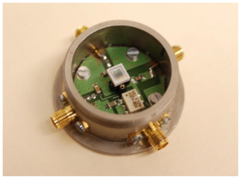
Holder for the radiation detector (crystal not shown). The SiPM is secured in the holder through header sockets and a light tight cover (not shown) is screwed on during tests.
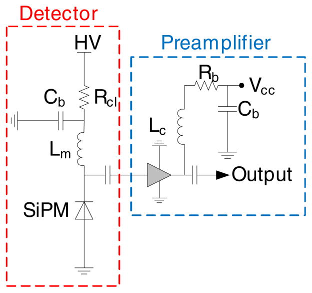
The circuit diagram of the detector and preamplifier is depicted in figure 2. At the detector side, the Rcl acts as a current limiting resistor, while Cb is the bypass capacitor (filter) for the power line. Lm here creates a high impedance path to drive the fast signals generated in the SiPM to the ac coupled amplifier. In the preamplifier circuit, Rb sets the bias current while Lc (optional) is a RF choke to minimize gain and power loss of the amplifier.
Figure 2.
Schematic for the detector (red dotted box) and preamplifier (blue dotted box).
3.2. Setup and data acquisition
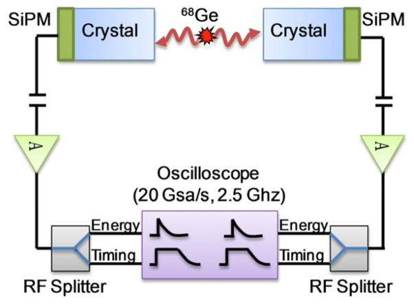
To measure the CRT between the two modules, they were placed ‘head-on’ with a Ge-68 source in between them as illustrated in figure 3. Outputs from PET detectors were fed to a high speed oscilloscope to digitize the signal waveforms. Radiation signals often ‘pile-up’ on SiPM dark counts, especially at higher bias voltages, causing baseline fluctuations that produce additional timing jitter of SiPM based detectors (Piemonte et al 2011). By acquiring raw signal waveforms of the detector, accurate time pick-off as described in the following sub-section can be implemented. It is important to note that high speed scopes have limited voltage resolution and can be a major source of noise when the digitizer input range is set to a high value. For example, the voltage resolution of the oscilloscope used in our measurement (Agilent DSO90254A) is 8 bits while the noise floor, known to be the lowest in the industry, is 1.27 mV RMS with a 800 mV input range and 183 μV RMS with a 80 mV input range. To circumvent this problem, we used an RF splitter to split the output of each amplifier into two paths; one for the acquisition of the whole waveform for energy information (with the digitizer input range set at 800 mV) and the other for determining the timestamp (with the digitizer input range set at 80 mV). The oscilloscope was programmed to trigger on the lower full-width-at-tenth-maximum bound of the 511 keV full energy photopeak coincident events and the waveforms from the timing channels were digitized for offline processing. Unless otherwise stated, all measurements were performed at room temperature.
Figure 3.
Setup for timing resolution measurements.
With this setup, the CRTs of three different scintillator pairs were measured and their geometries and surface treatments are summarized in table 1. The first pair (pair 1) consists of two 3 × 3 × 5 mm3 sized crystals that exactly match the 3 × 3 mm3 active area of the SiPMs. The second pair consists of two 3 × 3 × 20 mm3 sized crystals (pair 2), that is more relevant to clinical scanners due to their higher stopping power. As the active area of the SiPM is covered with a protective epoxy layer, crystals with smaller cross-section area were also chosen to optimize the light collected by the SiPMs (pair 3). A reflector that gives better timing performance for each of the respective crystal dimension has been selected (Spanoudaki and Levin 2011a).
Table 1.
Specifications of the scintillation crystals tested.
| Parameters | Pair 1 | Pair 2 | Pair 3 |
|---|---|---|---|
| Crystal | LYSO:Ce | LYSO:Ce | LSO:Ce |
| Size (mm3) | 3 × 3 × 5 | 3 × 3 × 20 | 2 × 2 × 3 |
| Surface treatment | All sides polished | All sides polished | Five sides polished |
| Reflector | Teflon | 3M ESR+ Teflon top | Teflon |
| Coupling grease | BC-630 | BC-630 | BC-630 |
3.3. Time pick-off
It is well known that for optimal timing performance, the triggering procedure should be performed at the first few detected scintillation photons. Therefore, acquiring partial waveforms from the timing channel which contain the initial pulse rising edge is sufficient for accurate timing. The rising edges of the signals were digitized at 20 GS s−1 (timing channel of figure 3) and the time pickoff method is similar to the method described by Vinke et al (2009). For each pulse, the baseline was determined by an averaging procedure using a small time window (500 ps) right before the onset of the rising edge. By doing so, baseline shifts induced by the SiPM dark counts are accounted for, enabling the operation of the SiPM at a high bias voltage. Figure 4 depicts the baseline determination process for a pair of coincident signals. Individual time stamps are then determined by leading-edge time pickoff using constant trigger levels on the rising edge with respect to the predetermined baselines and the time stamp differences are histogrammed and fitted to a Gaussian function to calculate the CRT.
Figure 4.
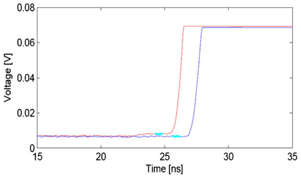
Digitized rising edge of typical photon pulses. The baseline is calculated using the average of the cyan colored data. A timing offset between the pulses has been added for clarity. Notice that the baseline of the red signal is shifted due to a dark count.
4. Results
4.1. Rise times
Figure 5 shows typical 511 keV full energy pulses with 3 × 3 × 5 mm3 crystals (pair 1) at 0.9 V overvoltage. From the figure, the rise time (10%–90%) is around 8–9 ns. The overvoltage (bias voltage over breakdown value) of each SiPM was determined by plotting the signal amplitude versus bias voltage curve with a low energy radiation source (to prevent saturation), and is defined as the zero-crossing value of the linear extrapolation of the curve.
Figure 5.
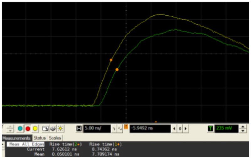
Screen capture of the high speed oscilloscope with rise time measurement of typical coincident full energy 511 keV annihilation photon pulses.
4.2. CRT of detector modules
The timing performance for the crystal pairs is summarized in figure 6. The best timing resolution for the 3 × 3 × 5 mm3 (pair 1) and 3 × 3 × 20 mm3 (pair 2) LYSO crystals were 147 ± 3 ps and 186 ± 3 ps, respectively, at 2.1 V overvoltage. In order to minimize light loss due to misalignment or through the SiPM epoxy layer, smaller LSO scintillators (2 × 2 × 3 mm3) were used and a CRT of 125 ± 2 ps was achieved at the same bias voltage.
Figure 6.
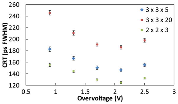
CRT of the various scintillation crystals used. The error bar is the Gaussian fitting error (2σ).
These timing resolutions were obtained by varying the trigger level over a fixed range (figure 4). The two-dimensional CRT map, with trigger threshold expressed in photon number, for the 2 × 2 × 3 mm3 LSO crystals (pair 3) at 2.1 V overvoltage is shown in figure 7. The single photon level was measured with the oscilloscope by triggering on the single photon level (dark counts) of the SiPMs without the crystals present to prevent signal contamination by the natural radioactivity of the lutetium-176 atoms.
Figure 7.
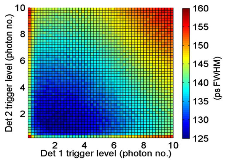
An example of a 2D CRT map as a function of trigger height for the 2 × 2 × 3 mm3 LSO crystals at 2.1 V overvoltage.
Finally, to validate the values obtained, one of the detector modules was moved on a manual translation stage away from the other detector and radiation source. The larger 3 × 3 × 5 mm3 crystals were used for this measurement (for higher count rate) and the movement was performed in three steps of 50 mm for a total of 100 mm. This test was carried out at 2.1 V overvoltage and triggered at the same threshold for all three measurements. The acquired CRT is shown in figure 8 and the time differences between two adjacent peaks are 166 ± 3 ps and 170 ± 3 ps which, using the speed of light, corresponds to 49.8 ± 0.9 mm and 51.0 ± 0.9 mm, respectively.
Figure 8.
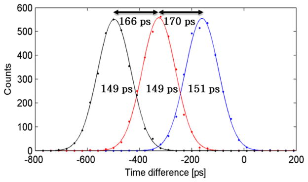
CRT of 3 × 3 × 5 mm3 LYSO crystals at three different positions (0, 50 and 100 mm).
4.3. CRT dependence on depth-of-interaction
Long crystals of about 20–30 mm are most commonly used in PET scanners for their ability to more efficiently stop the high energy gamma photons. Different orientations for timing resolution measurements have been reported such as irradiation on the side face of the crystal elements and read out with SiPM from one or both of the end faces (Cosentino et al 2012). Depending on the 511 keV photon depth-of-interaction (DOI), there is a variance in the arrival time of the scintillation photons due to propagation time variances within the crystal (Moses and Derenzo 1999, Spanoudaki and Levin 2011a). To investigate the effect of propagation time variance within the crystal on CRT, the setup was slightly modified as shown in figure 9. A SiPM coupled to the long 3 × 3 × 20 mm3 crystal, is irradiated from the side with reference to a small crystal (2 × 2 × 3 mm3). The source was placed closer to a long crystal under study to ensure that the irradiated area is small (~1.5 mm in this setup). DOI3 is an arbitrary position close to the SiPM and the source was moved in 5 mm steps along the length of the crystal for a total of four measurements (15 mm in distance).
Figure 9.
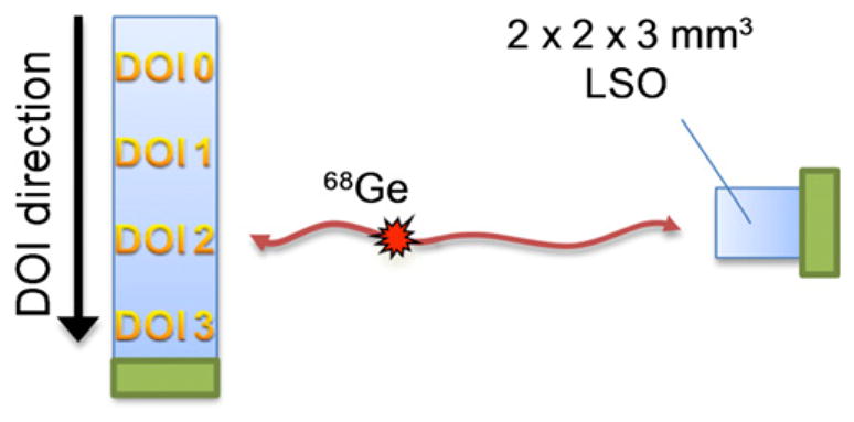
Setup for CRT measurement at various DOI positions.
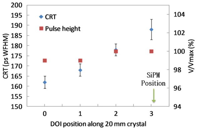
The results of this experiment are shown in figure 10. It was found that, although not intuitive, the timing resolution degraded with increasing DOI (i.e. decreasing distance to the photosensor). The CRT at DOI0 was 162 ± 3 ps while it was 188 ± 5 ps at DOI3. The average of full energy photopeak values at each DOI position, expressed in percentage of the maximum amplitude, is also plotted on the same figure.
Figure 10.
CRT and relative pulse height of the long 3 × 3 × 20 mm3 LYSO crystals along four DOI positions down its length.
To elucidate this phenomenon, a simulation was performed using DETECT 2000 for 20 mm long crystals using parameters described in table 1 (97% reflectance for reflector) and the result is illustrated in figure 11. Figure 11(left) shows the photon arrival time profile of 100K photons at the photosensor due to propagation effects when the light is emitted at 2 mm (representing DOI3 in figure 9) and 17 mm (DOI0) from the photosensor. When the exponential rise and decay time of the crystal (90 ps and 44 ns respectively) are taken into consideration and repeated with 100 million photons through Monte Carlo simulation, it resulted in the arrival time profile of figure 11(right). It is clear from the figure that the initial slope is dependent on the DOI within long crystals.
Figure 11.

Initial photon arrival profile (first 300 ps) due to propagation effects only (left) and when convolved with rise/decay scintillation response (right). In the right figure, the two curves have been superimposed for comparison of initial rising edge.
4.4. CRT variation with temperature
It is known that temperature has an effect on the properties of scintillation crystals (Feng et al 2010), SiPM (Buzhan 2001) and thermal noise of electronics (Rudolph et al 1999). To assess the effect of temperature on the timing performance of the setup, the two detector modules where attached to Peltier coolers and the CRT was measured. Results are summarized in figure 12, and the best CRT at 25.0 °C, 20.0 °C and 15.0 °C are 127 ± 2 ps, 123 ± 2 ps and 121 ± 3 ps respectively.
Figure 12.
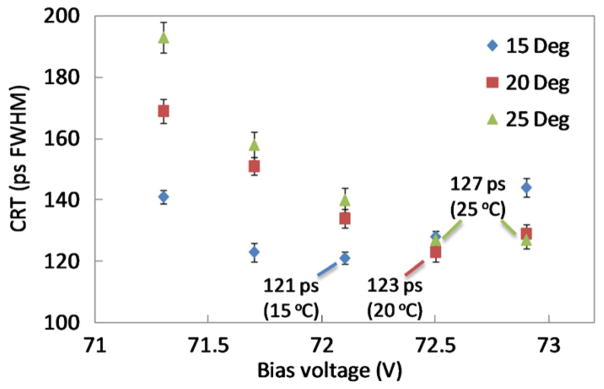
CRT of 2 × 2 × 3 mm3 LSO crystals with respect to bias voltages at three different temperatures. The x-axis is expressed in bias voltage rather than overvoltage as the breakdown voltage of a SiPM varies with temperature. The temperature is that of the Peltier surface and may be slightly higher at the SiPM.
5. Summary and discussion
As opposed to approaches to improve timing performance of the SiPM based detector by increasing the signal slope (equation (1)) through custom designed readout electronics, we show that it is possible to obtain excellent CRT using a commercially available low-noise RF amplifier. These amplifiers, based on the Darlington configuration, are fabricated with indium–gallium-phosphide (InGaP) heterojunction bipolar transistor (HBT) technology to provide wideband amplification with extremely low noise. The advantages of utilizing these amplifiers include: (1) ease of design—in many cases allowing them to be viewed as a black-box with an input, an output and a constant amplification factor, (2) lower noise figure and power consumption compared to more commonly used silicon based bipolar or CMOS technology at similar bandwidth, (3) availability of a wide range of products with various specifications to suit one’s application and (4) relatively low cost of these components due to their widespread use. On the other hand, these amplifiers are typically designed with 50 Ω input/output impedance to match 50 Ω transmission lines. Although this is useful for transmitting fast signals over long distances, this resistance forms a long RC decay constant with the SiPM capacitance, thereby reducing the slope of the signal. However, despite producing much slower signals than as reported in similar studies, a timing resolution comparable to the best reported value (Huizenga et al) has been achieved using similar crystals and SiPMs (figure 6). We expect that a photosensor with a smaller output capacitance would benefit most from this preamplifier design as such a detector would have both a fast signal rise time and low noise.
Another reason contributing to the superior timing resolution in this and other studies using waveform digitizers is due to the accurate baseline determination explained in section 3.3. Analogue time pick-off methods implementing fixed baseline thresholds, e.g. leading-edge timing with discriminator circuits and fast time-to-digital converters (TDC), would require higher triggering thresholds due to dark counts, especially at higher bias voltages, thereby degrading timing performance. Although waveform sampling is currently still costly, high-speed multichannel waveform digitizers are available (Ritt et al 2010) that can be implemented into multichannel block detectors for ToF PET. An interesting alternative ‘hardware’ approach to waveform sampling would be to implement filtering circuits that reduces the duration (pulse width) of a dark count, thereby reducing the probability of a signal pile-up on a dark count (Gola et al 2011). This approach, potentially more cost-effective by trading off versatility, would allow the use of simple discriminator circuits while suppressing timing resolution degradation due to dark counts pile-up. Further studies, however, would be required to assess the timing performance of this method compared to waveform sampling. It should also be noted that regardless of the time pick-off method used, further improvements in timing resolution of the SiPM based detectors can be achieved by using faster/brighter crystals like LaBr3 or calcium co-doped LSO (Szczesniak et al 2010) and also possibly by constructing rigid reflector structures to couple the light from 3 × 3 mm2 crystals to the active area of the SiPM.
The aspect ratio and surface treatment/reflector of a scintillator crystal directly determines the propagation temporal variance profile of light photons within the crystal and accordingly affects its timing resolution. I.e. the higher the variance (transit time spread), the poorer the timing resolution (Seifert et al 2012). This explains the poorer timing resolution for the 20 mm long crystal compared to the 5 mm long LYSO crystal. On the other hand, the 2 × 2 × 3 mm3 LSO crystals, despite having similar aspect ratio and properties as compared to the 3 × 3 × 5 mm3 LYSO crystal, produced better timing resolution. This confirms that a non-negligible amount of light is lost through spreading in the 200–300 μm thick protective epoxy layer over such devices.
Another interesting finding from this study was that for long crystals with specular reflectors, as reported in section 4.3, the timing resolution degraded with decreasing 511 keV photon interaction distance to the photosensor. A similar curve was also observed (but amplified) using two long crystals placed side by side and using a collimator to irradiate both crystals at the same DOI. This trend is attributed to the propagation effect within the crystal (Moses and Derenzo 1999) and is depicted in figure 11; when an interaction occurs deep in the crystal (close to the photosensor), about half of the light photons will be directed toward the SiPM while the other half will travel a longer distance only to reach the SiPM after being reflected at the other end of the crystal. This would, in effect, produce a bi-Gaussian-like distribution for the photon arrival time profile, implying that the amount of initial direct photon flux would be smaller. On the other hand, it can be assumed that scintillation light photons emitted from the other end away from the sensor will arrive at the photosensor in a single Gaussian photon arrival time profile, leading to a higher slope (dυ/dt) with an offset in time. The final output pulse of actual detectors, however, will further be shaped by the timing jitter of SiPMs and its large capacitance making them difficult to observe with a waveform digitizer. That said, we can infer that a head-on irradiation of a long crystal with higher stopping power, assuming all other factors were identical, would produce a small improvement in timing resolution compared to a crystal with smaller stopping power as more radiation photons will interact at shallow DOI. Likewise, head-on irradiated detector geometry (figure 3) would produce better timing resolution than side-irradiated/end-readout configurations for the same reason. However, with a different surface treatment or reflector with Lambertian reflectance such as Teflon tape, the results are expected to be considerably different. This is because as opposed to being directed in the same direction after a reflection with specular reflectors, the scintillation photons are diffused with each reflection, implying that light photons emitted far from the photosensor, on the average, will have to undergo more interactions before arriving at the face of the photosensor, leading to more light being lost due to imperfect reflector reflectivity.
Finally, we see little improvement of timing resolution over the temperature range tested and the reasons are as follows. (1) Crystal—the luminosity of L(Y)SO scintillators are known to generally increase at about 0.2%/K (Mao et al 2011) implying a small overall increase over the tested range. Furthermore, the decay time of the crystal may increase (Feng et al 2010). (2) SiPM—small decrease in PDE over the temperature range (Collazuol et al 2011); gain of SiPM as function of overvoltage has been shown to be independent from temperature and although dark counts are reduced at lower temperature (Lightfoot et al 2008, Ramilli 2009), this effect is less pronounced due to the baseline correction already being applied. The CRT curves, however, are shifted in voltage due to the change of breakdown voltage with temperature (Buzhan 2001). (3) Preamplifier—the improvement in electronics noise over this small temperature range can be assumed to be negligible (Rudolph et al 1999). Nonetheless, a more profound variation in timing resolution of SiPM based scintillator detectors can be expected for a greater temperature range (Goertzen et al 2012, Piemonte et al 2011).
6. Conclusion
In this paper, we show that, instead of designing custom preamplifiers that aim to maximize the output slope of SiPM based scintillators, excellent timing performance comparable to the best reported values so far can be achieved by utilizing commercial low noise RF amplifiers that minimize the noise contribution despite having a high 50 Ω input impedance. We also showed that the head-on irradiation of long scintillator detectors will produce better timing resolution compared to the side irradiated scheme and that lowering the temperature of the detectors by about 10 °C has little effect on improving the timing performance of such detectors.
This paper provided insights to optimize timing performance of SiPM based detectors, and the front-end electronics described, which are relatively easy to implement, would allow individuals with a basic to moderate electronics background to design ToF capable preamplifiers and/or facilitate setups for ToF detector designs and characterization.
Acknowledgments
This research is supported by the Stanford Dean’s Postdoctoral Fellowship, the Netherlands Organization for Scientific Research (NWO) and NIH-NIBIB grant R21EB014405.
References
- Auffray E, et al. A comprehensive & systematic study of coincidence time resolution and light yield using scintillators of different size, wrapping and doping NSS/MIC; IEEE Nucl Sci Symp Med Imag Conf; 2011. pp. 64–71. [Google Scholar]
- Buzhan P, et al. Large area silicon photomultipliers: performance and applications. Nucl Instrum Methods. 2006;A567:78–82. [Google Scholar]
- Buzhan P, et al. An advanced study of silicon photomultiplier. ICFA Instrum Bull. 2001;23:28–42. [Google Scholar]
- Campbell JC, et al. Recent advances in avalanche photodiodes. IEEE J Sel Top Quantum Electron. 2004a;10:777. [Google Scholar]
- Campbell JC, et al. Recent advances in avalanche photodiodes (addendum) IEEE J Sel Top Quantum Electron. 2004b;10:1446–7. [Google Scholar]
- Collazuol G, Bisogni MG, Marcatili S, Piemonte C, Del Guerra A. Studies of silicon photomultipliers at cryogenic temperatures. Nucl Instrum Methods. 2011;A628:389–92. [Google Scholar]
- Cooke DW, McClellan KJ, Bennett BL, Roper JM, Whittaker MT, Muenchausen RE, Sze RC. Crystal growth and optical characterization of cerium-doped Lu1.8Y0.2SiO5. J Appl Phys. 2000;88:7360–2. [Google Scholar]
- Cosentino L, Finocchiaro P, Pappalardo A, Garibaldi F. Characterization of a scintillating mini-detector for time-of-flight positron emission tomography with depth-of-interaction. Rev Sci Instrum. 2012;83:084302. doi: 10.1063/1.4739310. [DOI] [PubMed] [Google Scholar]
- Dorenbos P, de Haas JTM, van Eijk CWE. Gamma ray spectroscopy with a circle divide 19 × 19 mm(3) LaBr3: 0.5% Ce3 +scintillator. IEEE Trans Nucl Sci. 2004;51:1289–96. [Google Scholar]
- Farrell R, Olschner F, Shah K, Squillante MR. Advances in semiconductor photodetectors for scintillators. Nucl Instrum Methods. 1997;A387:194–8. [Google Scholar]
- Feng H, Jary V, Mihokova E, Ding DZ, Nikl M, Ren GH, Li HY, Pan SK, Beitlerova A, Kucerkova R. Temperature dependence of luminescence characteristics of Lu2(1-x)Y2xSiO5:Ce3+ scintillator grown by the Czochralski method. J Appl Phys. 2010;108:033519. [Google Scholar]
- Goertzen AL, Zhang X, Liu CY, Kozlowski P, Retiere F, Ryner L, Sossi V, Stortz G, Thompson CJ. Temperature dependence of a SiPM detector for an MR compatible PET system. Med Phys. 2012;39:4640. doi: 10.1118/1.4740189. [DOI] [PubMed] [Google Scholar]
- Gola A, Piemonte C, Tarolli A. Analog circuit for timing measurements with large area SiPMs coupled to LYSO crystals. IEEE Nucl Sci Symp Conf Rec. 2011:725–31. [Google Scholar]
- Grigoriev E, Akindinov A, Breitenmoser M, Buono S, Charbon E, Niclass C, Desforges I, Rocca R. Silicon photomultipliers and their bio-medical applications. Nucl Instrum Methods. 2007;A571:130–3. [Google Scholar]
- Huizenga J, Seifert S, Schreuder F, Dam HTv, Dendooven P, Löhner H, Vinke R, Schaart DRA. Fast preamplifier concept for SiPM based time-of-flight PET detectors. Nucl Instrum Methods. 2012;A695:379–84. [Google Scholar]
- Iams H, Salzberg B. The secondary emission phototube. Proc IEEE. 1935;23:55–64. [Google Scholar]
- Karp JS, Surti S, Daube-Witherspoon ME, Muehllehner G. Benefit of time-of-flight in PET: experimental and clinical results. J Nucl Med. 2008;49:462–70. doi: 10.2967/jnumed.107.044834. [DOI] [PMC free article] [PubMed] [Google Scholar]
- Kim CL. A way to improve timing resolution of SSPM: pulse shape of SSPM. Proc Int Workshop on New Photon-Detectors (Shinshu University, Japan) 2009:010. [Google Scholar]
- Kovaltchouk VD, Lolos GJ, Papandreou Z, Wolbaum K. Comparison of a silicon photomultiplier to a traditional vacuum photomultiplier. Nucl Instrum Methods. 2005;A538:408–15. [Google Scholar]
- Lightfoot PK, Barker GJ, Mavrokoridis K, Ramachers YA, Spooner NJC. Characterisation of a silicon photomultiplier device for applications in liquid argon based neutrino physics and dark matter searches. J Instrum. 2008;3:P10001. [Google Scholar]
- Mao RH, Zhang LY, Zhu RY. LSO/LYSO crystals for future HEP experiments. J Phys: Conf Ser. 2011;293:012004. [Google Scholar]
- Melcher CL, Schweitzer JS. Cerium-doped lutetium oxyorthosilicate—a fast, efficient new scintillator. IEEE Trans Nucl Sci. 1992;39:502–5. [Google Scholar]
- Moses WW. Time of flight in PET revisited. IEEE Trans Nucl Sci. 2003;50:1325–30. [Google Scholar]
- Moses WW, Derenzo SE. Prospects for time-of-flight PET using LSO scintillator. IEEE Trans Nucl Sci. 1999;46:474–8. [Google Scholar]
- Piemonte C, Gola A, Picciotto A, Pro T, Serra N, Tarolli A, Zorzi N. Timing performance of large area SiPMs coupled to LYSO using dark noise compensation methods. IEEE Nucl Sci Symp Conf Rec. 2011:59–63. [Google Scholar]
- Powolny F, et al. Time-based readout of a silicon photomultiplier (SiPM) for time of flight positron emission tomography (TOF-PET) IEEE Trans Nucl Sci. 2011;58:597–604. [Google Scholar]
- Ramilli M. Characterization of SiPM: temperature dependencies. IEEE Nucl Sci Symp Conf Rec. 2009:1742–5. [Google Scholar]
- Renker D. Geiger-mode avalanche photodiodes, history, properties and problems. Nucl Instrum Methods. 2006;A567:48–56. [Google Scholar]
- Renker D. New trends on photodetectors. Nucl Instrum Methods. 2007;A571:1–6. [Google Scholar]
- Renker D. New developments on photosensors for particle physics. Nucl Instrum Methods. 2009;A598:207–12. [Google Scholar]
- Ritt S, Dinapoli R, Hartmann U. Application of the DRS chip for fast waveform digitizing. Nucl Instrum Methods. 2010;A623:486–8. [Google Scholar]
- Riu J, Sicard M, Royo S, Comeron A. Silicon photomultiplier detector for atmospheric lidar applications. Opt Lett. 2012;37:1229–31. doi: 10.1364/OL.37.001229. [DOI] [PubMed] [Google Scholar]
- Rudolph M, Doerner R, Klapproth L, Heymann P. An HBT noise model valid up transit frequency. IEEE Electron Device Lett. 1999;20:24–6. [Google Scholar]
- Schaart DR, Seifert S, Vinke R, van Dam HT, Dendooven P, Lohner H, Beekman FJ. LaBr3:Ce and SiPMs for time-of-flight PET: achieving 100 ps coincidence resolving time. Phys Med Biol. 2010;55:N179–N89. doi: 10.1088/0031-9155/55/7/N02. [DOI] [PubMed] [Google Scholar]
- Seifert S, van Dam HT, Vinke R, Dendooven P, Lohner H, Beekman FJ, Schaart DR. A comprehensive model to predict the timing resolution of SiPM-based scintillation detectors: theory and experimental validation. IEEE Trans Nucl Sci. 2012;59:190–204. [Google Scholar]
- Shimizu S, Kurashige K, Usui T, Shimura N, Sumiya K, Senguttuvan N, Gunji A, Kamada M, Ishibashi H. Scintillation properties of Lu0.4Gd1.6SiO5: Ce (LGSO) crystal. IEEE Trans Nucl Sci. 2006;53:14–7. [Google Scholar]
- Spanoudaki VC, Levin CS. Photo-detectors for time of flight positron emission tomography (ToF-PET) Sensors. 2010;10:10484–505. doi: 10.3390/s101110484. [DOI] [PMC free article] [PubMed] [Google Scholar]
- Spanoudaki VC, Levin CS. Investigating the temporal resolution limits of scintillation detection from pixellated elements: comparison between experiment and simulation. Phys Med Biol. 2011a;56:735–56. doi: 10.1088/0031-9155/56/3/013. [DOI] [PubMed] [Google Scholar]
- Spanoudaki VC, Levin CS. Scintillation induced response in passively-quenched Si-based single photon counting avalanche diode arrays. Opt Express. 2011b;19:1665–79. doi: 10.1364/OE.19.001665. [DOI] [PubMed] [Google Scholar]
- Szczesniak T, Moszynski M, Syntfeld-Kazuch A, Swiderski L, Koschan MAS, Melcher CL. Timing resolution and decay time of LSO crystals Co-doped with calcium. IEEE Trans Nucl Sci. 2010;57:1329–34. [Google Scholar]
- van Loef EVD, Dorenbos P, van Eijk CWE, Kramer K, Gudel HU. High-energy-resolution scintillator: Ce3+ activated LaBr3. Appl Phys Lett. 2001;79:1573–5. [Google Scholar]
- Vinke R, Seifert S, Schaart DR, Schreuder FP, de Boer MR, van Dam HT, Beekman FJ, Lohner H, Dendooven P. Optimization of digital time pickoff methods for LaBr3-SiPM TOF-PET detectors. IEEE Nucl Sci Symp Conf Rec. 2009:2962–8. [Google Scholar]
- Wilmshurst TH. Signal Recovery from Noise in Electronic Instrumentation. Bristol: Hilger; 1990. [Google Scholar]


