Abstract
This paper proposes a two-step radio frequency (RF) sputtering process to form a ZnO film for pyroelectric sensors. It is shown that the two-step sputtering process with a lower power step followed by a higher power step can significantly improve the voltage responsivity of the ZnO pyroelectric sensor. The improvement is attributed mainly to the formation of ZnO film with a strongly preferred orientation towards the c-axis. Furthermore, a nickel film deposited onto the uncovered parts of the ZnO film can effectively improve the voltage responsivity at higher modulating frequencies since the nickel film can enhance the incident energy absorption of the ZnO layer.
Keywords: pyroelectric sensor, thin film deposition, ZnO
1. Introduction
Thin-film pyroelectric sensors have been successfully used in many applications, such as pollution monitoring, hot image detector, intruder alarm, and gas analysis [1-4]. They possess the advantages of being integrable with on-chip circuitry, un-cooled detecting, room-temperature operation, fast and wide spectral response with high sensitivity and low cost [2, 4-5]. The principle of thin-film ZnO pyroelectric sensors is based on the pyroelectric effect to convert the temperature variation to the corresponding electrical signal. The dynamic pyroelectric response current of thin film pyroelectric sensors can be described as [4]:
| (1) |
where η is the absorption coefficient of radiation, P is the pyroelectric coefficient of the pyroelectric film, A is the sensing area, dT/dt is the temperature variation rate of the pyroelectric film. The higher temperature variation rate in pyroelectric film leads to a higher response current of the pyroelectric sensor. In this paper, the ZnO film is adopted as the sensing element to generate the pyroelectric signal. The ZnO film formed by the proposed two-step sputtering process has been observed to possess the growth characteristic of strongly preferred orientation toward the c-axis, which has succeeded in the application of film bulk acoustic resonator (FBAR) [6].
The proposed ZnO pyroelectric sensor is fabricated by the process containing the backside-etching of silicon wafer, the dielectric layer deposition by low pressure chemical vapor deposition (LPCVD), the top and bottom electrodes deposition by e-beam evaporation, and the ZnO thin film deposition by radio frequency (RF) sputtering. The top electrode and the radiation absorption layer play very important roles in the overall performance of the pyroelectric sensor. According to the authors' published work [5], the partially covered electrode (PCE) can reveal a higher responsivity than that of fully covered electrode. The uncovered part of ZnO film is directly exposed to the heat source, which can greatly improve the responsivity of the pyroelectric sensor in virtue of increasing the energy absorption. Moreover, a nickel layer is deposited onto the un-covered parts of the ZnO film to enhance the incident energy absorption and thus to improve the sensor's dynamic response and device performance [7].
In the present ZnO pyroelectric sensor, a two-step RF sputtering process is used to deposit the ZnO film to improve the responsivity of ZnO pyroelectric sensors. The top electrodes cover the ZnO film partially. In addition, a nickel film deposited onto the uncovered part of the ZnO film is applied to enhance the absorption of incident energy. The experiment shows that the present fabrication process can significantly improve the performance of the ZnO pyroelectric sensor.
2. Fabrication Process
Figure 1 shows the fabrication process of the proposed ZnO pyroelectric sensor. A double-side polished p-type (100) silicon wafer is adopted as the substrate. Silicon nitride layers of thickness of 1 μm are deposited onto both sides of the substrate by LPCVD to obstruct the thermal conduction to the substrate, which can increase the pyroelectric signal and responsivity of the sensing element. Then photolithography and reactive ion etching (RIE) are used to pattern the etch window at the bottom side of the substrate, as shown in Figure 1(a). Subsequently, the KOH solution of 45 wt% is used to etch the substrate until the remaining thickness is about 50 μm. The etching temperature is kept at 75 oC. Therefore, a cavity shown in Figure 1(b) is formed at the bottom side of the substrate to reduce or block the thermal loss from the ZnO layer to the substrate and ambient.
Figure 1.
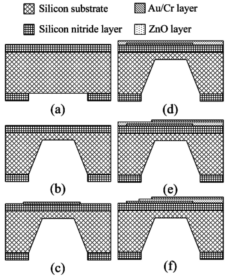
Fabrication process of the ZnO pyroelectric sensor.
The pyroelectric sensing element is consisted of a ZnO sensing layer sandwiched in between the bottom and top electrodes, and is accomplished on the top-side of the substrate. The bottom and top electrodes are both composed of gold and chromium. The chromium is an adhesion layer to promote the adhesion between the gold electrode and the substrate or ZnO. The thicknesses of gold and chromium are 100 nm and 10 nm, respectively. In the step shown in Figure 1(c), e-beam evaporation is used to deposit the bottom electrode and then patterned by wet etching. After the bottom electrode metallization, the ZnO layer of a thickness of 600 nm is deposited by RF magnetron sputtering, as shown in Figure 1(d). A ZnO target with 99.99% purity is adopted. The ZnO target is pre-sputtered for 15 minutes prior to the film deposition to remove any surface impurity. The chamber is pumped with base pressure up to 8×10⁻⁷ Torr before sputtering. The chamber is then filled with the mixture of argon and oxygen with the gas-mixing ratio of 5:3. The chamber pressure is 2×10⁻³ Torr while deposition. The substrate is heated up to 200°C while deposition, which can help to make better ZnO film quality. In the step of Figure 1(e), the fabrication of the top electrode is similar to that of the bottom electrode except that the top electrode is patterned by lift-off. Finally, the ZnO layer is etched to expose the bonding pad of the bottom electrode, as shown in Figure 1(f). The recipe of the etching solution is CH3COOH: H3PO4: H2O=1: 1: 10. Figure 2 shows the finished ZnO pyroelectric sensor.
Figure 2.

The finished ZnO pyroelectric sensor.
The sputtering RF power significantly affects the ZnO film quality, and therefore affects the responsivity of the ZnO pyroelectric sensor. We use two-step sputtering process under different RF powers to achieve a better responsivity of the pyroelectric sensor. Three different RF powers are adopted to investigate the influences of the RF power on the responsivities of the ZnO pyroelectric sensors, namely 90 W, 120 W, and 150 W. The three different RF power make up nine different ZnO sputtering processes, as shown in Table 1. The deposition rates of the three different RF powers are 1.22 nm/min for 90W, 2.02 nm/min for 120 W, and 2.63 nm/min for 150 W. For the two-step sputtering process, each step deposits a half of the required total ZnO film thickness. However, the samples No. 7–9 use a single power to deposit the required total ZnO film thickness.
Table 1.
The RF powers of ZnO film sputtering process.
| Sample group | RF power (W) | |
|---|---|---|
|
| ||
| Step 1 | Step 2 | |
| 1 | 120 | 90 |
| 2 | 120 | 150 |
| 3 | 90 | 120 |
| 4 | 90 | 150 |
| 5 | 150 | 90 |
| 6 | 150 | 120 |
|
| ||
| Single step | ||
|
|
||
| 7 | 90 | |
| 8 | 120 | |
| 9 | 150 | |
3. Experimental Setup
Figure 3 shows the schematic of the responsivity measurement of the proposed ZnO pyroelectric sensor. The radiation source is a calibrated He-Ne laser with 633 nm wavelength and 1mW maximum power. The laser beam is chopped at a modulated frequency (ω). The modulated beam is split into two beams by a prism. One is reflected on a photodiode as the reference, and the other one is defocused such that the beam spot can cover the whole top electrode of the ZnO pyroelectric sensor. The output voltage of the sensor is amplified by the SR560 low-noise voltage amplifier. Both the output signals of the sensor and the photodiode are recorded and displayed by a digital oscilloscope.
Figure 3.
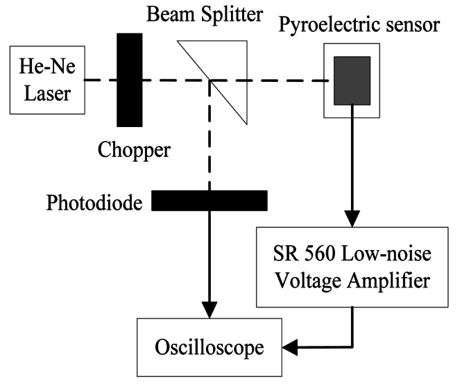
The experiment setup of responsivity measurement.
4. Results and Discussion
The voltage responsivity of pyroelectric sensor is related to the modulated frequency of pyroelectric sensor [8]. Figure 4 shows the responsivities to modulated frequencies of the test samples under the different sputtering processes listed in Table 1. The responsivity (Rv) is defined as the ratio of the output voltage of the sensor to the input power of the radiation source. Each particular colored bar in Figure 4 corresponds to one of the nine test sample groups listed in Table 1. The height of each colored bar represents the responsivity of the sensor under a particular sputtering process. In other words, the higher the colored bar is, the larger the responsivity is. Obviously, the two-step sputtering processes with a lower-power step followed by a higher-power step can significantly improve the responsivity of the ZnO pyroelectric sensor. Sample 2 (120W+150W) reveals the highest responsivity among the nine test sample groups. For the lower RF power step, the lower deposition rate can obtain finer grains. After the lower power step, the faster deposition rate of the higher RF power step can obtain strongly preferred columnar grains and eventually results in fine columnar grain structures. For the single-step sputtering processes (samples 7 to 9), Sample 8 with RF power of 120 W reveals the highest responsitivity among the three single-step sputtering processes. The responsivity of Sample 2 is about 2 to 4 times than that of Sample 8. Though the two-step power processes with a higher power step followed by a lower power step can also improve the responsivity, the improvements are insignificant.
Figure 4.
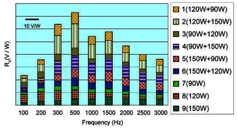
The voltage responsivities of the test samples under the different sputtering processes listed in Table 1.
We further deposit the nickel layers of thickness of 10 nm onto the uncovered parts of the ZnO layer, as shown in Figure 5. It should be mentioned that a gap of 20 μm, as shown in Figure 5(b), between the nickel layers and the top electrodes is required to prevent the increasing of resistance. The resistance of nickel is larger than that of gold. If the top electrodes contact with the nickel films, then the resulting resistance of the top electrodes will increase. Therefore, a gap between the nickel layers and the top electrodes is required to prevent the increasing of resistance. The nickel layer can enhance the radiation absorption and therefore improve the sensing performance. As shown in Figure 6, the enhanced nickel layer significantly improves the responsivity of the ZnO pyroelectric sensor for a higher modulated frequency. In general, the voltage responsivity of pyroelectric sensors will decline as the modulated frequencies increase. Therefore, one can use the nickel layer to enhance the energy absorption and thus reduce the decline of voltage responsivity at higher frequencies.
Figure 5.
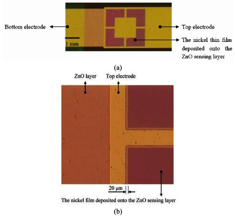
The finished ZnO pyroelectric sensor with 10 nm thick Ni layer deposited onto the ZnO sensing layer, (a) optical microscope with low magnification, and (b) optical microscope with high magnification.
Figure 6.
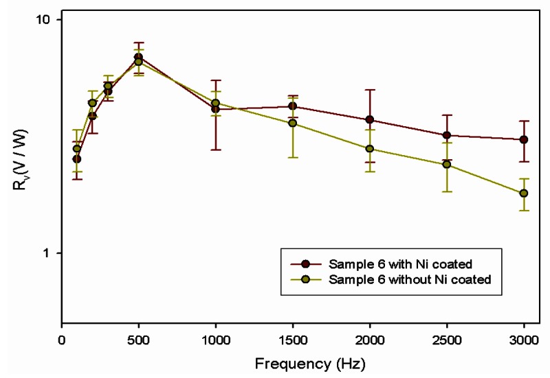
Voltage responsivity of the ZnO pyroelectric sensor with partially covered electrode under a thickness of 10 nm Ni layer deposited onto the bare ZnO sensing element.
5. Conclusions
The proposed two-step sputtering process can significantly improve the voltage responsivity of ZnO pyroelectric sensors. Not only the magnitudes of RF powers should be concerned, but also the sequence of the sputtering steps. The two-step sputtering processes with a lower-power step followed by a higher-power step can significantly improve the voltage responsivity. The improvement is mainly because that the formed ZnO film has a strongly preferred orientation towards the c-axis. Although the two-step power process with a higher power step followed by a lower power step can also improve the responsivity, the improvement is insignificant. The design of partial cover top electrodes can increase the energy absorption of the ZnO sensing layer. Furthermore, the deposition of nickel onto the ZnO layer can effectively overcome the disadvantage of the responsivity decline at higher frequencies since the nickel can enhance the energy absorption of ZnO. However, a sufficient space between the nickel layers and the top electrodes is required to prevent the increasing of resistance.
Acknowledgments
The authors are thankful for the financial support of this research from the National Science Council of Taiwan through the grant no. NSC 95-2221-E-211-008-MY2.
References and Notes
- 1.Porter S.G. A brief guide to pyroelectric and detectors. Ferroelectrics. 1980;33:193–216. [Google Scholar]
- 2.Chang C.C., Tang C.S. An integrated pyroelectric infrared sensor with a PZT thin film. Sensors and Actuators A. 1998;65:171–174. [Google Scholar]
- 3.Kohli M., Wuethrich C., Brooks K., Willing B., Forster M., Muralt P., Setter N., Ryser P. Pyroelectric thin-film sensor array. Sensors and Actuators A. 1998;60:147–153. [Google Scholar]
- 4.Li L., Zhang L., Yao X., Li B. Computer simulation of temperature field of multilayer pyroelectric thin film IR detector. Ceramics International. 2004;30:1847–1850. [Google Scholar]
- 5.Wei C.S., Lin Y.Y., Hu Y.C., Wu C.W., Shih C.K., Huang C.T., Chang S.H. Partial-electroded ZnO pyroelectric sensors for responsivity improvement. Sensors and Actuators A. 2006;128:18–24. [Google Scholar]
- 6.Park S.H., Seo B.C., Park H.D., Yoon G. Film bulk acoustic resonator fabrication for radio frequency filter applications. The Japan Society of Applied Physics. 2000;39:4115–4119. [Google Scholar]
- 7.Weiguo L., Jongsoo K., Weiguang Z. Influences of thin Ni layer on the electrical and absorption properties of PZT thin film pyroelectric IR sensors. Infrared Physics & Technology. 2000;41:169–173. [Google Scholar]
- 8.Zook J.D., Liu S.T. Pyroelectric effects in thin film. Journal of Applied Physics. 1978;49:4604–4606. [Google Scholar]


