Abstract
In this paper an input-output transfer function analysis based on the frequency response of a photometer circuit based on operational amplifier (op amp) is carried out. Op amps are universally used in monitoring photodetectors and there are a variety of amplifier connections for this purpose. However, the electronic circuits that are usually used to carry out the signal treatment in photometer circuits introduce some limitations in the performance of the photometers that influence the selection of the op amps and other electronic devices. For example, the bandwidth, slew-rate, noise, input impedance and gain, among other characteristics of the op amp, are often the performance limiting factors of photometer circuits. For this reason, in this paper a comparative analysis between two photodiode amplifier circuits is carried out. One circuit is based on a conventional current-to-voltage converter connection and the other circuit is based on a robust current-to-voltage converter connection. The results are satisfactory and show that the photodiode amplifier performance can be improved by using robust control techniques.
Keywords: photometer circuit, current-to-voltage converter connection, frequency response, robust control
1. Introduction
Semiconductor junctions convert the photon energy of light into an electrical signal by releasing and accelerating current-conducting carriers within the semiconductor [1]. This response is used to fabricate photodiodes and due to their characteristics and features they are used in many laboratory and industrial applications.
Some of the most important characteristics and features of photodiodes are their low cost, excellent linearity, good quality of the time domain performance, the speed of the their response, their low noise, they are compact and lightweight devices, and so on.
Also, photodiodes are used in safety equipment, blood particle analyzers, pulse oximeters, X ray detection, photographic flash control, light meters, automotive applications, optical communications, fiber optic links, and so on.
However, depending on the kind of application, the electronic circuits used to monitoring photodiodes should meet some specific requirements. For example, in laboratory applications, where the temperature is held constant, the responsivity, the shunt resistance, the shunt capacitance and the dark current of the photodiode, which are all temperature dependent photodiode parameters, do not vary from their expected values, and the response of the photodiode is satisfactory if the users guarantee that the power supply is stable and that there are not any noise or disturbance sources corrupting the response of the photodiode. In this kind of applications, conventional photometer circuits perform satisfactorily and designers do not have to work hard in order to meet the final user requirements.
On the other hand, in industrial applications, where photometer circuits have to work under severe working conditions such as the endurance of high temperatures, high humidity, dangerous chemical attacks, undesirably strong vibrations, pollution, and so on [2], designers are faced with real-world problems that they cannot control and that corrupt the response of photometer circuits tremendously. In this kind of applications, the design requirements that the designers have to meet are much more exigent than the ones of the above-mentioned kind of applications, and the designers cannot guarantee a good performance of the photometer circuits unless they use robust and optimal control techniques [3, 4] to the design of the signal treatment stages of the photometers.
Generally speaking, in practice the signals produced by sensors are frequently corrupted by noise that cause sensor operations to deviate from their true value, which causes an undesirable degree of uncertainty in the measurements carried out by the sensors. Therefore, in order to cancel the noise that corrupts the relevant information coming from sensors, robust and optimal signal treatment stages are needed [5-15].
The present paper is aimed at showing the importance of the application of the above-mentioned techniques to the design of photometer circuits, and it also shows the importance of the frequency response analysis in order to provide insights into the benefits and trade-offs of the current-to-voltage converter connections usually used to build linear photometer circuits.
2. The photo effect and photodiode model
According to Graeme [1], light entering a semiconductor material produces an electrical current by releasing hole-electron pairs. There, photons transfer energy to the atoms of the radiated material, moving these hole and electron carriers to the radiated material, moving these hole and electron carriers to their conductions states. Once there, the individual carriers may or may not contribute to current flow.
Carriers released within the depletion region of a semiconductor junction produce the majority of this current due to the electric field of this region. That region contains ionized or depleted atoms that support a voltage differential across the junction. The associated electric field accelerates the carriers toward the terminals of the diode, adding conduction energy to the carriers and reducing the probability of recombination. Applying reverse bias to the junction expands the depletion region to encompass more of the material of the diode within the accelerating field [1].
Forward bias narrows the depletion region and lowers the barrier to carrier injection. Diffusion component of current greatly increases and drift component decreases. Carrier density is large (exponential), making the junction conductive and allowing a large forward current.
In photodiodes, semiconductor doping levels and the junction depth are two of the most important parameters. The depth and extent of the junction determines the location of the depletion region and the light wavelengths that produce an efficient response. Photons generate carriers at a range of depths with a given range proportional to the photon wavelength [1].
The most important characteristics of a photodiode are the following [1, 16, 17]:
Spectral response
Radiometric sensitivity
Responsitivity
Quantum efficiency
Sensitivity
Linearity
Dark current
Shunt resistance
Junction capacitance
Reverse breakdown voltage
Open circuit voltage
Response time
Noise current
Angular response
Package style
Also, according to [1, 16, 17], the equivalent circuit for a photodiode is shown in Fig. 1, where IP is light generated photocurrent, IN is noise current, RSH is the shunt resistance, RS is the series resistance, CJ is the junction capacitance, and RL is an external load resistance connected to the photodiode.
Figure 1.
Equivalent circuit for a photodiode connected to a load resistance
3. The photometer circuits
Due to their excellent linearity, gain accuracy, high input resistance, high open-loop gain, low noise, low offsets and wide bandwidth, among other characteristics, operational amplifiers are commonly used in monitoring photodiodes [1, 16-18].
In addition, the energy transmitted by light to a photodiode can be measured as either a voltage or a current output, and when the photodiode output is monitored as a voltage, the response has a logarithmic relationship to the light energy received since the sensitivity of the diode varies with its voltage. Nevertheless, when a linear relationship between the photodiode response and the light energy received is desired, the voltage drop across the photodiode is held constant for a fixed sensitivity and the photocurrent is linearly related to the incident light energy [1, 16-18].
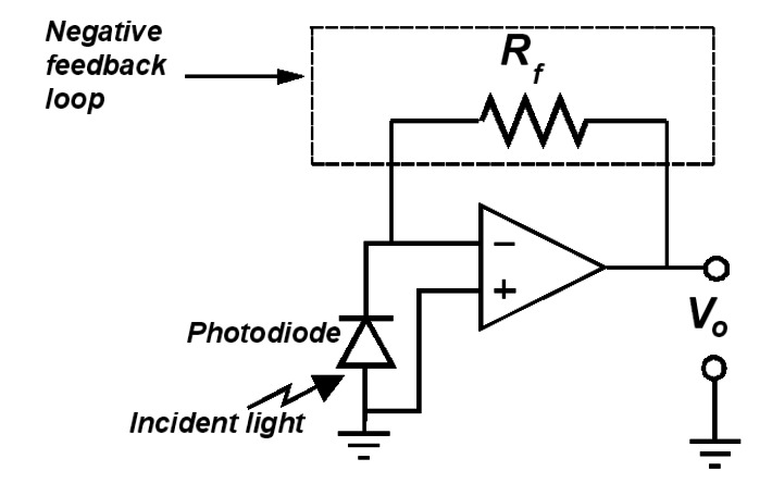
However, according to [19, 20], in spite of the fact that there are a variety of amplifier connections used for monitoring photodiodes, most of them are based on the basic current-to-voltage converter (CVC) connection shown in Fig. 2, in which the photodiode output is monitored as a current. In this figure, Rf is the negative feedback resistor used to convert the photocurrent into an output voltage linearly related to the light energy. This optoelectronic circuit is used in both integrated circuits containing a photodiode and a transimpedance amplifier on a single chip, and in discrete designs.
Figure 2.
Conventional current-to-voltage converter connection.
According to [20], the circuit shown in Fig. 2 has both advantages and disadvantages. On the one hand, if the photodiode exhibits very good characteristics and the ambient temperature is held constant at the optimum value, this circuit provides a very high quality output voltage.
On the other hand, in the field, outside the laboratory or in applications in which the temperature is not constant, as the responsivity, the shunt resistance, the junction capacitance and the dark current of the photodiode are temperature dependent, and the noise is dependent upon the characteristics of the photodiode and the operating conditions, the uncertainty of measurement of linear photometer circuits based on conventional CVC connections, as the one shown in Fig. 2, increases. Therefore, photometer circuits based on conventional CVC connections are not robust [3, 4].
From the Control Engineering point of view, in Fig. 2, the sensor is placed in an open-loop system in which the feedback network cannot reject the negative effects of the disturbance and noise that corrupt the relevant information coming from the photodiode. Therefore, changes in the ambient temperature, uncertainties and noise in the electrical components, noise coming from the power supply, and so on, make the output of the system to deviate considerably from its true value.
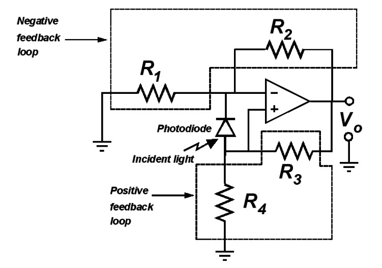
In [19-21], a robust photometer circuit is presented taking into consideration the fact that in order to improve the disturbance rejection performance of the circuit, the photodiode should be placed in a robust feedback compensation network. The robust photometer circuit is shown in Fig. 3.
Figure 3.
Robust photometer circuit.
The analysis of the relative error between the theoretical sensitivity and the experiemental sensitivity of the circuit shown in Fig. 3 is carried out in [19]. Also, a detailed analysis of the sensitivity of the photometers shown in Fig. 2 and Fig. 3 to photodiode parameter variations is carried out in [20], ending with a comparative analysis between the performance of the robust circuit and the performance of the non-robust one.
In addition, in [22] a simplified analysis of the effect of the offset voltage of the op amp on the response of these photometers is presented. Furthermore, in [22] both the low-frequency noise power estimation analysis and the total harmonic distortion performance analysis of the circuits shown in Fig. 2 and Fig. 3 are carried out.
Finally, in [21] a complete analysis of the influence of the op amp parameters on the performance of the circuit in Fig. 3 is done, along with the analysis of the stability region of such a circuit.
However, there is al least one more type of analysis that should be carried out to these circuits. This is the frequency response analysis by using an input-output transfer function approach. This is the aim of the next section.
4. Frequency response analysis by using an input-output transfer function approach
According to [4], the frequency response analysis can be used to describe the response of a system to sinusoids of varying frequency, ω [rad/s]. This kind of analysis has the advantage of being directly linked to the time domain, and at each frequency the transfer function has a clear physical interpretation. Also, one important advantage of a frequency response analysis of a system is that it provides insight into the benefits and trade-offs of feedback control.
According to [4], the most important design objectives which necessitate trade-offs in feedback control are the following:
Performance, good disturbance rejection: loop-transfer function, L(s), large
Performance, good command following: L(s) large
Stabilization of unstable plant: L(s) large
Mitigation of measurement noise on plant outputs: L(s) small
Small magnitude of input signals: controller transfer function, K(s), small and L(s) small
Physical controller must be strictly proper: K(s) → 0 and L(s) → 0 at high frequencies
Nominal stability: L(s) small
Robust stability: L(s) small
where s = jω.
Fortunately, the above-mentioned conflicting design objectives are generally in different frequency ranges, and most of the objectives can be met by using a large loop gain (|L(jω)| > 1) at low frequencies below crossover, and a small gain (|L(jω)| < 1) at high frequencies above crossover [4].
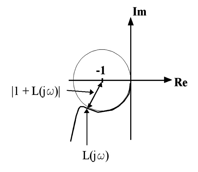
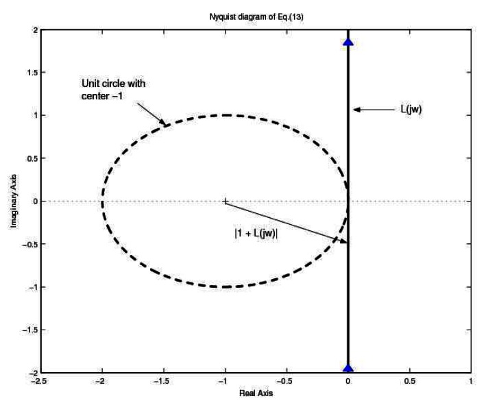
Furthermore, in accordance with the loop-shaping approach to controller design [3, 4], a system is robust if the following stability margins are guaranteed: a gain margin (GM) equal to infinity, a gain reduction margin equal to 0.5, and a minimum phase margin (PM) of 60°. Graphically, for a single-input-single-output (SISO) system, it means that the Nyquist plot of the loop transfer function of the system will always lie outside the unit circle with center -1 in the complex plane (see Fig. 4) [3, 4].
Figure 4.
Nyquist plot of L(jω) for robust stability.
However, robust stability must not be confused with robust performance [3, 4]. A system that is robust could have noise rejection problems. That is to say, measurement noise, high frequency noise and some kind of perturbations can corrupt the relevant information coming from it. Nevertheless, a system that has robust performance characteristics has robust stability and has a satisfactory noise rejection performance, among other good properties.
According to [20], assuming that the op amp is ideal (see [21] for the case of the non-ideal op amp), the transfer function of the circuit shown in Fig. 2 from IP(s) to Vo(s) is given by
| (1) |
where RSH ‖ RS is the parallel equivalent of RSH and RS. And the transfer function of the circuit shown in Fig. 3 from IP(s) to Vo(s) is given by
| (2) |
where
| (3) |
| (4) |
| (5) |
| (6) |
| (7) |
| (8) |
| (9) |
| (10) |
As can be seen from the above equations, (2) is much more complex than (1). However, (1) cannot deal satisfactorily with disturbances and uncertainties in the parameters of the photodiode, something that is done by (2) satisfactorily [20].
Here, in order to carry out a practical analysis of the reason why the above statement is true taking into consideration the GM and the PM of (1) and (2), the photometer circuits were implemented by using the Siemens silicon photodiode BPW21, with RS = 10 Ω and RSH = 100 kΩ and CJ equal to 580 pF for a reverse voltage of 0 V applied across the BPW21.
In addition, in the laboratory experiments the incident light came from the 3 mW RS Modulated Laser Diode Module 194-004, whose nominal wavelength is 670 nm, and the experimental sensitivity of the BPW21 at 670 nm was 0.1345 A/W. Furthermore, in order to have a 10 V output for a 3 mW input to the circuits shown in Fig. 2 and Fig. 3, Rf was chosen to be equal to 24.783 kΩ, and R1, R2, R3 and R4 were chosen to be equal to 1 kΩ, 100 Ω, 100 kΩ and 22.08 kΩ, respectively.
For the above-given values,
| (11) |
and
| (12) |
The loop transfer function of the robust photometer circuit [20] is
| (13) |
Thus, the sensitivity function of the robust circuit is
| (14) |
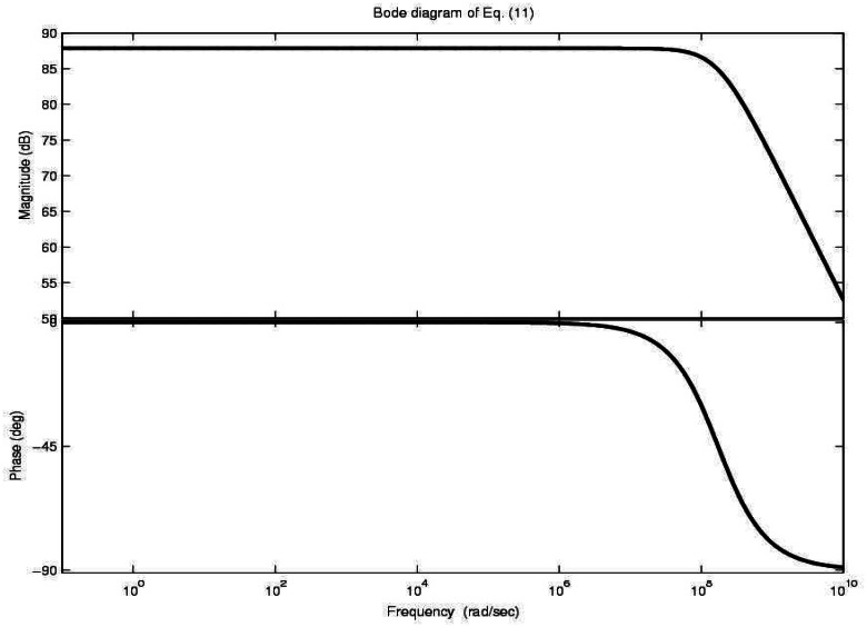
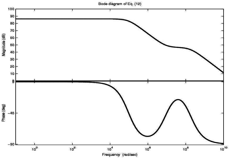
Moreover, the Bode plots of (11) and (12) are shown in Fig. 5 and Fig. 6, respectively. From these figures it can be seen that both closed-loop transfer functions have a similar characteristic at low frequencies, and that the robust circuit has a feedback controller that introduces lead-lag compensations at middle frequencies. These compensations improve the disturbance rejection performance of the photometer circuit.
Figure 5.
Bode plot of the closed-loop transfer function of the non-robust photometer (11).
Figure 6.
Bode plot of the closed-loop transfer function of the robust photometer (12).
The Nyquist diagram of the loop transfer function of the robust photometer (13) is shown in Fig. 7. Note that Lr(s) never enters the unit circle, which means that the closed-loop system with the transfer function given by (12) is robust. For this system, the stability margins are the following: GM = ∞ and PM = 90°.
Figure 7.
Nyquist diagram of the loop transfer function of the robust photometer (13).
The state-space representation of the SISO system given by (12) is the one given by
| (15) |
| (16) |
where x(t) is the state vector (size 2-by-1), u(t) is the input of the system (size 1-by-1) and y(t) (size 1-by-1) is the output of the system. Also, A, B, C and D are given below
| (17) |
| (18) |
| (19) |
| (20) |
Thus, the relationship between (12) and (15)-(16) is given by
| (21) |
where I is the identity matrix of size 2-by-2.
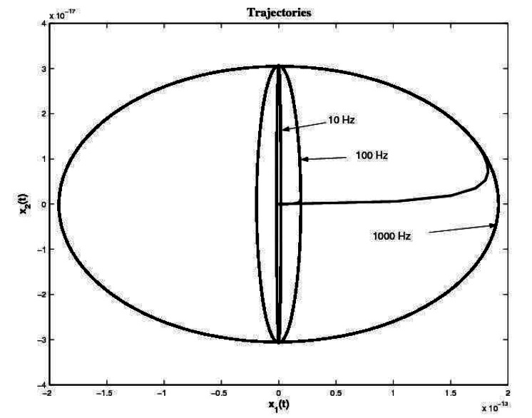
For the system given by (15)-(16), if the initial condition of the state vector x(t) = [x1(t) x2(t)]T is equal to x(0)=[0 0]T and the input u(t) is a sinusoid of varying frequency from 1 Hz on, the trajectories of the state variables of this state-space representation is the superposition of many ellipses, one ellipse for each frequency under consideration, with variable length axes. Fig. 8 shows the trajectories of the state variables of the above system for an input of 3 mW of incident light at 10 Hz, 100 Hz and 1 kHz, respectively. Note the fast, satisfactory convergence of the phase variables (i.e., x1(t) and x2(t)) of system. If the initial condition of the state vector of the system is not zero, the trajectory described by the state variables will converge to one similar to the ones shown in Fig. 8 (MATLAB simulation).
Figure 8.
Trajectories of the state variables of the system given by (15)-(16) for an input of 3 mW of incident light at 10 Hz, 100 Hz and 1 kHz, respectively.
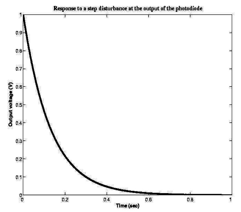
The response (MATLAB simulation) of the robust closed-loop system to a step disturbance in the sensitivity function (14) is shown in Fig. 9. From that figure it can be seen that step disturbances at the output of the plant are rejected satisfactorily. The closed-loop system does not amplify disturbances, its response does not have any oscillatory performance and its response decreases in amplitude very fast.
Figure 9.
Response of the robust photometer circuit to a step disturbance at the output of the photodiode.
5. Experimental results
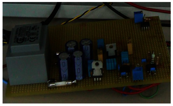
The photometer circuits presented in this paper (Fig. 2 and Fig. 3) were implemented in the laboratory with the photodiode BPW21, the resistors given in Section 4 and the op amp OP 07. Fig. 10 shows the practical implementation.
Figure 10.
Practical implementation of the circuits shown in Fig. 2 and Fig. 3.
Furthermore, in order to test the noise rejection performance of both circuits, a 3 mW incident light input signal at 0 Hz and wavelength equal to 670 nm was apply to the above-mentioned circuits, and the power spectrum of the output voltage of these circuits was displayed by using the YOKOGAWA Digital Oscilloscope DL9040.
The result of the experiment was that for the non-robust circuit the peak value of the power spectral density (PSD) of the noise of the output voltage was equal to -50.54 dBV. However, the peak value of the PSD of the noise of the output voltage was equal to -62.00 dBV. Therefore, a signal-to-noise ratio improvement of 10 dBV was achieved by using the robust compensation.
Moreover, the temperature coefficient (TC) of the output voltage of the robust photometer circuit was equal to -21.83 μV/°C, while the TC of the output voltage of the non-robust photometer circuit was equal to -40.16 μV/°C, which shows the importance of the application of robust control techniques to improve the performance of photometer circuits.
6. Conclusions
In this paper, an input-output transfer function analysis of a photometer circuit based on an op amp has been carried out. The results of the analysis showed the importance of the application of robust control technique to improve the performance of photometer circuits, and showed some of the most important points to be taken into consideration when designing these circuits for applications in which they have to work under severe working conditions, as it happens in most industrial applications.
Moreover, here two photometer circuits, one based on a conventional CVC connection and another based on a robust CVC connection, have been compared with each other. The results of such a comparison showed that the performance of photometer circuits based on robust CVC connections is much better that the performance of photometers circuits based on conventional CVC connections.
The use of robust control techniques to the design of complex sensor systems can bridge the gap between advanced signal conditioning techniques and the design of sensors for a wide range of applications. The reality is that only by the fusion of these concepts can the designer find the way clear to build the sensors that today's industry needs.
Acknowledgments
This work was supported by the Universidad Politecnica de Madrid, Spain.
References
- 1.Graeme J. Photodiode amplifiers: op amp solutions. McGraw-Hill; New York: 1996. [Google Scholar]
- 2.Hernandez W. A survey on optimal signal processing techniques applied to improve the performance of mechanical sensors in automotive applications. Sensors. 2007;7:84–102. [Google Scholar]
- 3.Zhou K., Doyle J. C., Glover K. Robust and Optimal Control. Prentice-Hall, Upper Saddle River; New Jersey: 1996. [Google Scholar]
- 4.Skogestad S., Posthlethwaite I. Multivariable Feedback Control. John Wiley and Sons; England: 1996. [Google Scholar]
- 5.Hernandez W. Improving the response of an accelerometer by using optimal filtering. Sensors and Actuators A. 2001;88:198–208. [Google Scholar]
- 6.Hernandez W. Improving the response of several accelerometers used in a car under performance tests by using Kalman filtering. Sensors. 2001;1:38–52. [Google Scholar]
- 7.Hernandez W. Improving the response of a wheel speed sensor using an adaptive line enhancer. Measurement. 2003;33:229–240. [Google Scholar]
- 8.Hernandez W. Improving the response of a wheel speed sensor by using frequency-domain adaptive filtering. IEEE Sensors Journal. 2003;3:404–413. [Google Scholar]
- 9.Hernandez W. Robust multivariable estimation of the relevant information coming from a wheel speed sensor and an accelerometer embedded in a car under performance tests. Sensors. 2005;5:488–508. [Google Scholar]
- 10.Hernandez W. Improving the response of a rollover sensor placed in a car under performance tests by using a RLS lattice algorithm. Sensors. 2005;5:613–632. [Google Scholar]
- 11.Hernandez W. Improving the response of a wheel speed sensor by using a RLS lattice algorithm. Sensors. 2006;6:64–79. [Google Scholar]
- 12.Hernandez W. Improving the response of a load cell by using optimal filtering. Sensors. 2006;6:697–711. [Google Scholar]
- 13.Hernandez W. Wheel speed sensors. In: Grimes C. A., Dickey E. C., Pishko M. V., editors. Encyclopedia of Sensor. vol. 10. American Scientific Publishers; 2006. pp. 461–472. [Google Scholar]
- 14.Hernandez W. Optimal estimation of the acceleration of a car under performance tests. IEEE Sensors Journal. 2007;7:392–400. [Google Scholar]
- 15.Hernandez W. Optimal estimation of the relevant information coming from a variable reluctance proximity sensor placed in a car undergoing performance tests. Mechanical Systems and Signal Processing. 2007;21:2732–2739. [Google Scholar]
- 16.Johnson M. Photodetection and measurement: maximizing performance in optical systems. McGraw-Hill; New York: 2003. [Google Scholar]
- 17.Pallàs-Areny R., Webster J. G. Sensors and signal conditioning. John Wiley & Sons; New Yok: 2001. [Google Scholar]
- 18.Burr-Brown Application Bulletin: Photodiode Monitoring with Op Amps, SBOA035 (AB-075) Available from: < http://focus.ti.com/lit/an/sboa035/sboa035.pdf>.
- 19.Hernandez W. Photometer circuit based on positive and negative feedback compensations. Sensor Letters. 2007;5:612–614. [Google Scholar]
- 20.Hernandez W. Linear robust photometer circuit. Sensors and Actuators A. 2007 doi: 10.3390/s90403149. Accepted for publication. [DOI] [PMC free article] [PubMed] [Google Scholar]
- 21.Hernandez W. Performance analysis of a robust photometer circuit. IEEE Transactions on Circuits and Systems-II. 2007 Accepted for publication. [Google Scholar]
- 22.Hernandez W. Robustness and noise voltage analysis in two photometer circuits. IEEE Sensors Journal. 2007;7:1668–1674. [Google Scholar]


