Abstract
We demonstrate an optoelectronic tweezer (OET) coupled to a lensfree holographic microscope for real-time interactive manipulation of cells and micro-particles over a large field-of-view (FOV). This integrated platform can record the holographic images of cells and particles over the entire active area of a CCD sensor array, perform digital image reconstruction to identify target cells, dynamically track the positions of cells and particles, and project light beams to trigger light-induced dielectrophoretic forces to pattern and sort cells on a chip. OET technology has been previously shown capable of performing parallel single cell manipulation over a large area. However, its throughput has been bottlenecked by the number of cells that can be imaged within the limited FOV of a conventional microscope objective lens. Integrating lensfree holographic imaging with OET solves this fundamental FOV barrier, while also creating a compact on-chip cell/particle manipulation platform. Using this unique platform, we have successfully demonstrated real-time interactive manipulation of thousands of single cells and micro-particles over an ultra-large area of e.g., 240 mm2 (i.e. 17.96 mm × 13.52 mm).
Introduction
Approaches for noncontact manipulation of cells and microparticles play important roles in miniaturized systems for chemical and biological analysis.1, 2 Versatile manipulation mechanisms utilizing optical, electrical, magnetic, and acoustic forces have already been demonstrated in the literature.3–5 Optoelectronic tweezers (OET) forms an approach that utilizes light-induced dielectrophoretic forces (DEP) for parallel cell manipulation using light images projected onto a low cost amorphous silicon coated glass.6–8 OET allows users to reconfigure projected light patterns in real-time for dynamic and parallel manipulation of various biological, micro- and nano-particles including DNA molecules9, 10, proteins11, sperm cells12, bacteria13, mammalian cells14–17, polystyrene beads7, semiconductor microdisks18, nanowires19, carbon nanotubes20, 21 and droplets22, 23. Phototransistor-based OET also enables cell manipulation in physiological buffers24. Floating-electrode OET enables the manipulation of aqueous droplets in electrically insulation media22. Researchers have also explored different photoconductive materials in OET such as P3HT:PCBM, one of the promising organic solar-cell materials, and organic photoconductive materials such as titanium oxide phthalocyanine 25, 26.
The operation principle of OET is based on light-induced dielectrophoretic forces on a photoconductive substrate. A light beam projected on an OET device optically generates extra electrons and holes to increase local photoconductivity, which creates light-patterned virtual electrodes and non-uniform electric fields to generate dielectrophoretic forces on cells and particles. Types of light sources that have been used for triggering and patterning virtual electrodes are versatile, from laser beams27, DMD projectors7, LCD displays28, to LED pixels29. OET platform can provide ultra-large area manipulation (i.e., > 100 cm2) since the technologies required to fabricate large panel OET and large display panel for driving OET already exist in e.g., display industry.
Although large-scale manipulation has been achieved on OET platforms, most manipulations, however, are passive. It means projected light patterns are pre-programmed before knowing where the objects are. Examples of passive type OET manipulations include optical conveyers, concentric-ring cell concentrators, comb-shape particle sorters, scanning line sorters, and many others7, 15. A major drawback of passive type manipulation is that it cannot selectively pick up target cells and micro-particles within a randomly distributed population since cell locations are unknown and no pre-programmed optical patterns can be generated in advance. On the other hand, there are also various active-type manipulation methods, where cells and beads are observed under a lens-based microscope, and light beams are projected to trap, transport, or pattern target cells identified based on their optical signatures such as size, texture, and fluorescence spectrum30. The current major bottleneck of active manipulation in OET is that the small field-of-view (FOV) of objective lenses limits the imaging and manipulation throughput. In order to resolve the image of each individual cell, an objective lens with a magnification higher than e.g., 10× isrequired. The FOV of a 10× objective lens is typically less than 1 mm2, and the FOV decreases with the increase of magnification. As a result, the number of cells that can be simultaneously observed and manipulated under a microscope is limited. This is one of the major technical barriers for parallel active cell manipulation on OET.
To overcome such FOV bottleneck, here we demonstrate a novel platform that integrates OET with lensfree holographic on-chip microscopy, an emerging technique that eliminates the need for an objective lens for ultra-large-area imaging. In this approach we utilize the lensfree holographic images captured on a CCD to reconstruct the microscopic images of cells and particles.31 This wide-field holographic microscopy technique has been demonstrated with numerous biological applications including blood analysis,32 waterborne parasite screening,33 and male fertility testing.34 Recently, deeply sub-micron resolution (e.g., ~0.3 μm),35, 36 and three-dimensional imaging and tracking capability37–40 have also been demonstrated with this holographic imaging approach. Such a lensfree on-chip microscopy technique furnishes OET with a complementary detection and imaging function to enable large-area, programmable, and parallel light-induced DEP manipulation of microscopic particles or cells with real-time position feedback.
Methods
Device and experimental setup
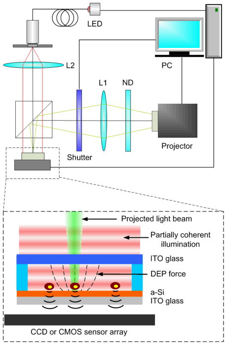
The experimental setup and the schematic configuration of an OET platform integrated with lensless holographic microscopy are shown in Fig. 1. An OET device is directly placed on top of the protective glass of an image sensor array, either a CCD or CMOS imager. The OET device consists of two transparent indium tin oxide (ITO) plane electrodes with the bottom electrode coated with a 50 nm n+ a-Si:H and a 1 μm intrinsic a-Si:H as the photoconductive layer. Cells and particles in aqueous solution are sandwiched between these two electrodes separated by a 100 μm thick spacer. A 10 Vpp ac voltage at a frequency of 100 kHz is applied to the top and the bottom ITO electrodes to power the OET chip.
Fig.1.
Schematic diagram of the experimental setup of OET integrated with lensfree holographic microscopy. An OET device is directly placed on a CCD or CMOS sensor array. The sensor array coupled with a partially coherent light source creates an on-chip holographic microscope with a field of view that is equal to the sensor array active area. With the microscopic information of particles, interactive OET manipulation of target objects is achieved by projecting light beams next to the targets. A computer with a customized LabView program is used to control and synchronize different modules.
Cell and particle manipulation on OET is based on light induced dielectrophresis. In the dark area without light illumination, the electrical impedance in the a-Si:H layer is large and little voltage drops across the aqueous layer. No DEP forces are produced. When a light beam illuminates the a-Si layer, it decreases the local impedance in the a-Si:H layer by generating extra electrons and holes for electrical conduction. This creates a light-patterned electrode that shifts the major voltage drop to the liquid layer. This induces non-uniform electric fields and DEP forces to attract or repel cells and particles near a light spot. By moving a light beam, the position of the virtual electrode and thus the induced electric field pattern changes in real-time to achieve dynamic cell and particle manipulation.
A commercial DMD-based projector (MP730, BenQ Inc.) is used in our experiments to provide dynamic optical images required to trigger light-induced dielectrophoretic forces for parallel cell and particle manipulation. The original projection lens set and the color filter wheel on the projector are removed and replaced with custom-built optics to generate controllable optical patterns matching the active OET manipulation region on chip.
To integrate lensfree holographic microscopy on OET, an 850-nm LED coupled to an optical fiber is used to create a partial coherent light source. This infrared LED is chosen since its wavelength can penetrate through the 1 μm thick a-Si:H layer that is not transparent to visible light. The light source illuminates the OET chip from above with a vertical distance of 10 cm. The senor array used in the experiment is a charge-coupled-device (CCD) image sensor chip (KAF-8300, Kodak) with a pixel size of 5.4 μm and an active area of 17.96 mm × 13.52 mm. When the scattered light waves from objects interfere with the unperturbed waves from the LED light source, the holograms of objects are formed and recorded by the CCD. Because the detection area of this lensfree imaging system is only limited by the active area of a CCD or CMOS (Quickcam Pro 9000, Logitech) sensor array, this imaging technique eliminates the FOV limitation in conventional microscopes imposed by objective lenses, which can be as large as e.g., 18 cm2.36 Therefore, parallel monitoring of hundreds of thousands of cells using this detection approach can be achieved.
Detection and manipulation algorithm
To achieve automated, real-time, interactive manipulation of randomly distributed cells and particles across a large area, the communication and synchronization between OET manipulation and lensfree holographic imaging is critical. The lensfree imaging system is responsible for imaging, identifying, and tracking every individual cell in a population within the active detection area. The locations of target cells identified are sent to the OET manipulation system to generate optical beams to manipulate the target cells. The manipulation and imaging systems form a closed feedback loop system with real-time cell position identification and cell actuation functions. The manipulation functions can be versatile, depending on users’ need. It can be collecting target cells to one or multiple desired locations, trapping and transporting target cells to form desired patterns, and various others.
LabView (National Instrument, USA) is employed to develop this close-loop, automatic, and interactive manipulation in our experiments. It is used to control the image recording, the image analysis, and the generation of projection optical patterns for OET manipulation (Fig. 2). The loop process begins by capturing a holographic image from the CCD image sensor. The raw holographic images can be analyzed by two different methods to determine the positions of cells in every holographic frame: (1) A pattern-matching algorithm which compares the recorded holograms to a prepared texture library 41; or (2) a holographic reconstruction process that generates microscopic images of detected objects.42
Fig. 2.
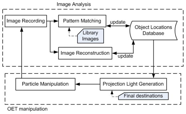
Process chart of the integrated close-loop OET manipulation and lensfree imaging system. One loop contains two periods, i.e., image analysis and OET manipulation. During the image analysis period, the system captures a raw image using a CCD or a CMOS sensor array to identify the target objects and their locations. Once the locations of the targets are determined, the OET system projects light beams to 5 manipulate the selected targets to their final destinations.
Method (1) is based on the concept of correlation index which simply evaluates the similarity of a recorded lensfree hologram to a mean library image of a given object type. With the defined object library image L(x′,y′), a 2D deviation map (Dev(x,y)) can be calculated for the recorded image f(x,y) by:
where DL represents the domain of the library image. After this step, the 2D deviation map is converted into a 2D correlation map for each object type by using:
where DevMAX and DevMIN refer to the maximum and minimum of the deviation values for f(x,y). After the creation of this 2D correlation map, potential candidates with large correlation peak values can be distinguished by setting a certain threshold value. The coordinates of the correlation peaks determine the positions of detected particles. The type of these particles can be identified by finding the maximum correlation after matching their holographic patterns with library images of various particle types. Further discussion on this detection and tracking related techniques can be found in the reference 41.
Different from the method discussed above, method (2) uses a digital algorithm to convert the lensfree holograms of micro-particles and cells back to their microscopic images before comparing them with library images. Two different levels, coarse and full image reconstruction, were conducted in our experiments for different purposes. To speed up the image analysis process during real-time manipulation, coarse reconstruction images (without twin-image elimination procedures36) were used for rapid particle tracking during real-time manipulation. This level of reconstruction is achieved by, first, decomposing the complex field by fast Fourier transform (FFT) into components with various spatial frequencies on the CCD plane. Then each component is multiplied with its corresponding transfer function component to simulate the effect of wave propagation in a uniform medium back to the object plane. Lastly, the modified frequency components are converted into a complex field through an inverse-FFT operation representing the microscopic images of micro-objects in real space.
Fully reconstructed images without twin-image artifacts can be used for particle identification when the images obtained by the coarse procedures above are not sufficient. Full image reconstruction can be done by further refining coarse images with an iterative recovery process. More details of this holographic imaging technique can be found in reference 42.
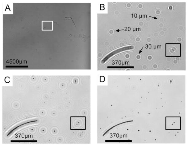
Out of this reconstruction process, method (2) provides microscope-like images of objects (example Fig. 3C and Fig. 3D), whose coordinates are determined by calculating their centroids using the intensity profile of the reconstructed images. The type of detected objects can be identified by analyzing the morphological properties of their reconstructed images (e.g., size, intensity, and eccentricity). Since the images reconstructed by this method do not overlap as much as the holograms in method (1), this approach is especially suitable for analyzing samples containing higher density of micro-objects.
Fig. 3.
(A) A full field-of-view of the holographic image showing a mixture containing 10, 20, and 30 μm polystyrene beads. (B) The holographic image of the selected area in (A). (C) The coarse and (D) the full reconstruction images of the lensfree hologram shown in (B). (B), (C) and (D) show two different methods used to determine the locations of the objects. In (B), the locations of objects can be determined by matching the holograms with a library of lensfree images. In (C) and (D), the particle types are distinguished by their sizes, determined through their reconstructed lensfree images.
According to the object coordinates determined by either of the two methods discussed above, our custom-designed LabView program can compare new object coordinates with previous ones to update the object location database. In our system, the program only searches over the whole FOV for potential candidates in the first frame. Starting from the second frame, searching is limited to the neighbourhood of each target object identified in the previous frame. This searching strategy reduces the time for image analysis and allows rapid particle tracking during real-time interactive manipulation. Based on the location database and the desired final locations of objects, the program creates a projection light pattern to induce DEP forces on target micro-objects (e.g., particles or cells) over a period of time. Target micro-objects will be moved toward the preset locations during the time when projection light illuminates. The same procedures repeat themselves after the acquisition of each holographic frame until all target particles are transported to their final desired locations.
Results and Discussions
Recognition and tracking of micro-objects
To test the performance of our system, polystyrene particles with diameters of 10, 20, and 30 μm were mixed and suspended in an aqueous medium with electrical conductivity adjusted to 0.01S/m using potassium chloride (KCl). This mixture was introduced into the OET device placed onto a CCD array (see Fig. 1). An example holographic image of this particle mixture over a FOV of 17.96 mm × 13.52 mm is showed in Fig. 3A. Fig. 3B shows the raw hologram of a small region in the full FOV. Target particles can be identified by matching each particle’s hologram with a mean library image established by averaging 20 images of target type of particles (recorded with the same wavelength at the same depth position). Fig. 3C and Fig. 3D compare the image qualities obtained by the coarse and full reconstruction methods. The 10, 20, and 30 μm particles can be clearly recognized by directly measuring their sizes in their corresponding reconstructed images. The centroids of particles were determined by our custom-designed LabView program. These results illustrate that our holographic detection process can successfully separate nearby particles even when their lensfree hologram textures overlap with each other. For example, two holograms of 20 um particles shown in the circled area in Fig. 3B overlap and could not be identified by the direct hologram pattern-matching method, but could be separated and identified in Fig. 3C and 3D using digital reconstruction procedures.
Once objects were recognized as targets, the system followed a pre-defined strategy (Fig. 2) to create light spots to manipulate target particles in parallel. In OET manipulation, cells or micro-particles can be actuated either by positive or negative DEP forces, depending on particles’ relative polarizabilities compared to the surrounding media. Particles experiencing positive DEP forces are attracted to strong electric field regions, meaning moving towards light spots. On the contrary, particles with negative DEP forces are repelled by light spots. Micron-sized polystyrene particles typically experience negative DEP forces in aqueous media.
Interactive manipulation with lensfree hologram pattern matching method
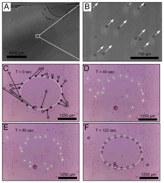
An example of parallel interactive manipulation of 901 20-μm particles randomly distributed across a 17.96 mm × 13.52 mm area using the direct hologram pattern matching method is illustrated in Fig. 4A. Part of the image is enlarged in Fig. 4B to show that every recognized particle is pushed to move in one direction (pointed by arrows) by dynamic light patterns projected on the OET chip.
Fig. 4.
(A) A full field-of-view holographic image showing parallel interactive manipulation of 901 target particles. (B) The zoom-in image of (A). (C)–(F) Snapshots of sequential holographic images demonstrating that the selected particles in a random population can be manipulated to form an elliptical pattern. These particles were recognized through pattern matching within the first frame. The arrows show the directions and final destinations that the target particles are programmed to move toward. The light spots in (C) and (D) show the OET system tracing and manipulating the target micro-objects. After 122 seconds, most of the targets were moved to their desired destinations. The color images were recorded by the CMOS sensor array.
Fig. 4C to Fig. 4F are the snapshots of holographic images showing that a group of selected 20-μm particles were first recognized, then programmed to move to target locations, and eventually formed an elliptical pattern (Fig. 4F). These particles were recognized by pattern matching method in the first cycle. The time for analysis of the entire FOV is ~6 sec on the current setup. Starting from the second cycle, particle tracking is achieved by searching the neighbourhoods of objects identified in the first cycle, which reduced the feedback control cycle time to ~2.0 sec. The whole process from Fig. 4C to 4F takes ~122 seconds. The average particle speed during this manipulation process is ~25 μm/sec. The square light spots shown in Fig. 4D and 4E are for visualization purposes. In real operation, the projection light patterns will be automatically turned off during the image acquisition step to avoid perturbing the holographic patterns recorded on the sensor array.
In our platform, the particle-moving speed can be affected by several factors. First, it is affected by the light intensity of optical patterns projected on the OET chip. Light intensity controls the on-off status of virtual electrodes on OET. Second, the relative distance between the projected light spots and the centroid of holograms is also critical. The edge of a virtual electrode usually has the highest electric field gradient to generate larger DEP forces on particles. The fastest particle moving speed is achieved by always positioning target particle at the edge of a virtual electrode during the dynamic moving process (Fig. 4D and 4E). Third, the ratio of the image analysis period to the OET manipulation period in each cycle is another factor affecting particle speed. Image analysis period includes image recording time and the computational time for particle tracing (Fig. 2). The total computational time required for tracking targets is proportional to the area of the search and the number of targets. From Fig. 4C to Fig. 4F, the system monitored the neighbourhood of 20 target objects, which reduced the image analysis time from ~6 sec to ~0.5 sec, giving a relatively long manipulation period in each feedback cycle. If the manipulation period is long, a particle moves a longer distance in each loop, which increases the range of searching neighborhood for tracking an individual particle. This could increase the time required for image analysis and the chance of losing the particle. In general, to ensure faster particle movement and lower chance of losing particles, hardware performance and particle recognition algorithm are both critical to minimize the image analysis time in each cycle.
Interactive manipulation with lensfree holographic image reconstruction method
An example of real-time interactive manipulation using the image reconstruction approach for particle recognition is shown in Fig. 5. Two different sizes of polystyrene beads, 10 μm and 30 μm, were mixed in a KCl solution with conductivity adjusted to 0.01 S/m. In this manipulation example, the system is programmed to select some 30 μm beads, marked with squares in Fig. 5B and Fig. 5C, from this mixture and transport them to desired locations. Image reconstruction was performed in every raw holographic image during the manipulation. Two different levels of image reconstruction were conducted in the experiment. One is full image reconstruction that takes longer computation time (implementing twin-image elimination36) but yields more spatial details for each particle and can be performed in the first cycle of manipulation. Once target particles are identified, the image reconstruction function switches to the coarse mode, which requires shorter computation time, for rapid particle tracing and gives a longer period for particle movement in a cycle during the dynamic manipulation process. Although the coarsely reconstructed image exhibit twin-image artefacts, it is sufficient for particle tracing application. To ensure that the system does not lose track of target particles with the coarse approach, full reconstruction can always be performed during or at the end of the manipulation cycle. The average speed in Fig. 5 is ~1.3μm/sec. In this experiment, the average loop time is ~2.0 sec and the image analysis period is ~1.5 sec. The reconstruction time for a coarse image is ~1.2 sec, which increases the image analysis period in each cycle and reduces the average velocities. The velocity can be improved by adjusting the ratio of the image analysis period to the particle manipulation period.
Fig. 5.
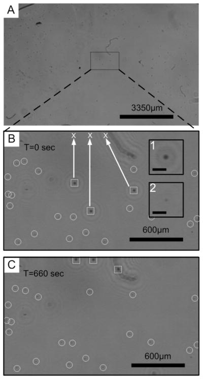
(A) A full field of view of reconstructed image with a mixture of 10 and 30 μm particles. (B) A digitally zoomed reconstructed image. The squares show the initial positions of the three selected 30-μm particles. The circles point to 10-μm particles. 30-μm particles were selected to move to the final destinations marked by crosses. The inset 1 and 2 are the enlarged images of 30 and 10-μm particles respectively. The scale bars are 90 μm. (C) The final positions of the particles after OET manipulation.
Cell manipulation
Human ovarian cancer cells (HeLa cells) were also used in this work to verify the platform’s ability to manipulate live biological cells. HeLa cells were cultured in Dulbecco’s modified Eagle’s medium (DMEM), supplemented with 10% fetal bovine serum (Hyclone), 50 mg/ml penicillin/streptomycin, and 50 mg/ml L-Glutamine. During the experiment, the cells were first washed with phosphate buffered saline (PBS, pH7.4) and then dissociated using 1X trypsin. After washed and neutralized with PBS, cells were re-suspended into isotonic buffer (8.5% sucrose [wt/vol], 0.3% dextrose [wt/vol]). The conductivity of the cell suspension was adjusted to 100 μS cm−1 in this isotonic buffer. The cell suspension was injected into the OET chip and placed on the system for characterization. To determine the locations of HeLa cells and distinguish them from other micro-objects in the chamber, the holographic textures of potential candidates were matched to a mean library cell image (Method (1) – see the Methods section).
Fig. 6 shows the sequential holographic images of a single HeLa cell been dragged towards a desired location during real-time feedback manipulation. Unlike polystyrene beads, HeLa cells experienced positive DEP force, so the cell hologram followed the projection light spot. The LabView program kept on updating the location of the cell to determine the position of the new projection spot. Therefore, the cell closely followed the designed path (defined by the light spot) toward the target destination. The average velocity of the HeLa cell is ~ 4.2μm/sec.
Fig. 6.
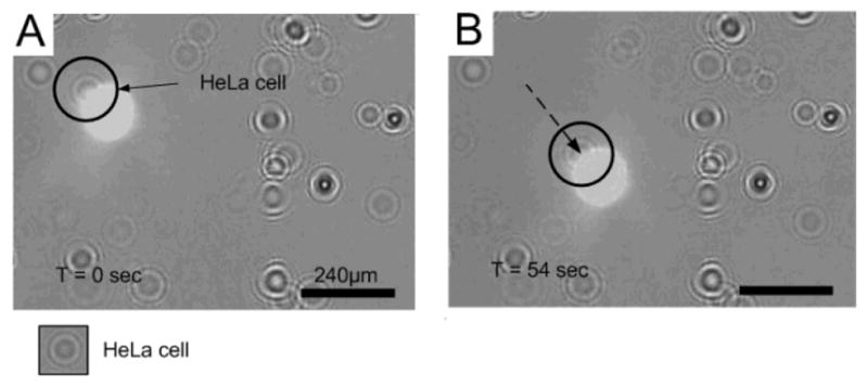
Sequential holographic images of a single HeLa cell attracted by a projected light spot and dragged toward the desired location.
Conclusions
We have demonstrated an optoelectronic tweezers (OET) platform integrated with a lensfree holographic microscope for large area, real-time, interactive, parallel manipulation of single cells and micro-particles. Lensfree imaging solves the fundamental small field of view limitation in conventional interactive manipulation in OET system. It can provide real-time position feedback of hundreds of thousands of cells randomly dispersed across a large area. In this integrated system, we have accomplished real-time interactive manipulation over an area of 2.40 cm2, which is two orders of magnitude larger than conventional microscope based OET platforms. Methods of automated pattern matching and image reconstruction have been demonstrated for monitoring thousands of objects inside our imaging and manipulation FOV. Real-time closed-loop manipulation of polystyrene particles and human ovarian (HeLa) cells has been successfully demonstrated using this high-throughput holographic on-chip microscope-integrated OET system.
Acknowledgments
Chiou lab gratefully acknowledges the support of the NSF CAREER AWARD ECCS 0747950, ECCS-1232279 and DBI 0852701. Ozcan Lab gratefully acknowledges the support of the Presidential Early Career Award for Scientists and Engineers (PECASE), ARO Young Investigator Award, NSF CAREER Award (Biophotonics program), ONR Young Investigator Award and the NIH Director’s New Innovator Award DP2OD006427 from the Office of The Director, NIH. Authors would also like to thank Chimei-Innolux Inc. for supporting the fabrication of OET chips.
Notes and references
- 1.Albrecht DR, Underhill GH, Wassermann TB, Sah RL, Bhatia SN. Nature methods. 2006;3:369–375. doi: 10.1038/nmeth873. [DOI] [PubMed] [Google Scholar]
- 2.El-Ali J, Sorger PK, Jensen KF. Nature. 2006;442:403–411. doi: 10.1038/nature05063. [DOI] [PubMed] [Google Scholar]
- 3.Ding X, Lin SCS, Kiraly B, Yue H, Li S, Chiang IK, Shi J, Benkovic SJ, Huang TJ. Proceedings of the National Academy of Sciences. 2012. [DOI] [PMC free article] [PubMed] [Google Scholar]
- 4.Adams JD, Kim U, Soh HT. Proceedings of the National Academy of Sciences. 2008;105:18165–18170. doi: 10.1073/pnas.0809795105. [DOI] [PMC free article] [PubMed] [Google Scholar]
- 5.Hu X, Bessette PH, Qian J, Meinhart CD, Daugherty PS, Soh HT. Proceedings of the National Academy of Sciences of the United States of America. 2005;102:15757. doi: 10.1073/pnas.0507719102. [DOI] [PMC free article] [PubMed] [Google Scholar]
- 6.Wu MC. Nature Photonics. 2011;5:322–324. [Google Scholar]
- 7.Chiou PY, Ohta AT, Wu MC. Nature. 2005;436:370–372. doi: 10.1038/nature03831. [DOI] [PubMed] [Google Scholar]
- 8.Hwang H, Park JK. Lab Chip. 2010;11:33–47. doi: 10.1039/c0lc00117a. [DOI] [PubMed] [Google Scholar]
- 9.Chiou PY, Ohta AT, Jamshidi A, Hsu HY, Wu MC. Microelectromechanical Systems, Journal of. 2008;17:525–531. doi: 10.1109/JMEMS.2008.916335. [DOI] [PMC free article] [PubMed] [Google Scholar]
- 10.Hoeb M, Rädler JO, Klein S, Stutzmann M, Brandt MS. Biophysical journal. 2007;93:1032–1038. doi: 10.1529/biophysj.106.101188. [DOI] [PMC free article] [PubMed] [Google Scholar]
- 11.Hwang H, Park JK. Analytical chemistry. 2009;81:9163–9167. doi: 10.1021/ac9021709. [DOI] [PubMed] [Google Scholar]
- 12.Ohta AT, Garcia M, Valley JK, Banie L, Hsu HY, Jamshidi A, Neale SL, Lue T, Wu MC. Lab on a Chip. 2010;10:3213–3217. doi: 10.1039/c0lc00072h. [DOI] [PubMed] [Google Scholar]
- 13.Chiou PY, Chang Z, Wu MC. A novel optoelectronic tweezer using light induced dielectrophoresis. 2003. [Google Scholar]
- 14.Ohta AT, Chiou PY, Han TH, Liao JC, Bhardwaj U, McCabe ERB, Yu F, Sun R, Wu MC. Microelectromechanical Systems, Journal of. 2007;16:491–499. [Google Scholar]
- 15.Ohta A, Chiou P, Phan H, Sherwood S, Yang J, Lau A, Hsu H, Jamshidi A, Wu M. Selected Topics in Quantum Electronics, IEEE Journal of. 2007;13:235–243. [Google Scholar]
- 16.Valley J, Neale S, Hsu H, Ohta A, Jamshidi A, Wu M. Lab on a Chip. 2009;9:1714. doi: 10.1039/b821678a. [DOI] [PMC free article] [PubMed] [Google Scholar]
- 17.Huang KW, Sattar S, Zhong JF, Chou CH, Tsai HK, Chiou PY. Advances in OptoElectronics. 2011:2011. [Google Scholar]
- 18.Tien M, Ohta A, Yu K, Neale S, Wu M. Applied Physics A: Materials Science & Processing. 2009;95:967–972. [Google Scholar]
- 19.Jamshidi A, Pauzauskie PJ, Schuck PJ, Ohta AT, Chiou PY, Chou J, Yang P, Wu MC. Nat Photon. 2008;2:86–89. doi: 10.1038/nphoton.2007.277. [DOI] [PMC free article] [PubMed] [Google Scholar]
- 20.Pauzauskie PJ, Jamshidi A, Valley JK, Satcher JH, Wu MC. Appl Phys Lett. 2009;95:113104–113103. doi: 10.1063/1.3212725. [DOI] [PMC free article] [PubMed] [Google Scholar]
- 21.Lee K, Lee SS, Lee JA, Lee KC, Ji S. Appl Phys Lett. 2010;96:013511. [Google Scholar]
- 22.Park S, Pan C, Wu T, Kloss C, Kalim S, Callahan C, Teitell M, Chiou E. Appl Phys Lett. 2008;92:151101. doi: 10.1063/1.2906362. [DOI] [PMC free article] [PubMed] [Google Scholar]
- 23.Park SY, Kalim S, Callahan C, Teitell MA, Chiou EPY. Lab on a Chip. 2009;9:3228–3235. doi: 10.1039/b909158k. [DOI] [PubMed] [Google Scholar]
- 24.Hsu H-y, Ohta AT, Chiou P-Y, Jamshidi A, Neale SL, Wu MC. Lab on a Chip. 2010;10:165–172. doi: 10.1039/b906593h. [DOI] [PubMed] [Google Scholar]
- 25.Yang SM, Yu TM, Huang HP, Ku MY, Hsu L, Liu CH. Opt Lett. 2010;35:1959–1961. doi: 10.1364/OL.35.001959. [DOI] [PubMed] [Google Scholar]
- 26.Wang W, Lin YH, Wen TC, Guo TF, Lee GB. Appl Phys Lett. 2010;96:113302–113303. [Google Scholar]
- 27.Neale S, Mazilu M, Wilson J, Dholakia K, Krauss T. Opt Express. 2007;15:12619–12626. doi: 10.1364/oe.15.012619. [DOI] [PubMed] [Google Scholar]
- 28.Choi W, Kim SH, Jang J, Park JK. Microfluid Nanofluid. 2007;3:217–225. [Google Scholar]
- 29.Zarowna-Dabrowska A, Neale SL, Massoubre D, McKendry J, Rae BR, Henderson RK, Rose MJ, Yin H, Cooper JM, Gu E. Optics Express. 2011;19:2720–2728. doi: 10.1364/OE.19.002720. [DOI] [PubMed] [Google Scholar]
- 30.Valley JK, Ohta AT, Hsu HY, Neale SL, Jamshidi A, Wu MC. Biomedical Circuits and Systems, IEEE Transactions on. 2009;3:424–431. doi: 10.1109/TBCAS.2009.2031329. [DOI] [PMC free article] [PubMed] [Google Scholar]
- 31.Isikman SO, Greenbaum A, Lee M, Bishara W, Mudanyali O, Su TW, Ozcan A. Analytical Cellular Pathology. 2012;35:229–247. doi: 10.3233/ACP-2012-0057. [DOI] [PMC free article] [PubMed] [Google Scholar]
- 32.Seo S, Isikman SO, Sencan I, Mudanyali O, Su TW, Bishara W, Erlinger A, Ozcan A. Analytical chemistry. 2010;82:4621–4627. doi: 10.1021/ac1007915. [DOI] [PMC free article] [PubMed] [Google Scholar]
- 33.Mudanyali O, Oztoprak C, Tseng D, Erlinger A, Ozcan A. Lab Chip. 2010;10:2419–2423. doi: 10.1039/c004829a. [DOI] [PMC free article] [PubMed] [Google Scholar]
- 34.Su TW, Erlinger A, Tseng D, Ozcan A. Analytical chemistry. 2010. [DOI] [PMC free article] [PubMed] [Google Scholar]
- 35.Bishara W, Su TW, Coskun AF, Ozcan A. Optics Express. 2010;18:11181–11191. doi: 10.1364/OE.18.011181. [DOI] [PMC free article] [PubMed] [Google Scholar]
- 36.Greenbaum A, Luo W, Su T-W, Göröcs Z, Xue L, Isikman SO, Coskun AF, Mudanyali O, Ozcan A. Nature Methods. 2012:9. doi: 10.1038/nmeth.2114. [DOI] [PMC free article] [PubMed] [Google Scholar]
- 37.Su TW, Isikman SO, Bishara W, Tseng D, Erlinger A, Ozcan A. Optics Express. 2010;18:9690–9711. doi: 10.1364/OE.18.009690. [DOI] [PMC free article] [PubMed] [Google Scholar]
- 38.Isikman SO, Bishara W, Mavandadi S, Yu FW, Feng S, Lau R, Ozcan A. Proceedings of the National Academy of Sciences. 2011;108:7296. doi: 10.1073/pnas.1015638108. [DOI] [PMC free article] [PubMed] [Google Scholar]
- 39.Isikman SO, Bishara W, Zhu H, Ozcan A. Appl Phys Lett. 2011;98:161109. doi: 10.1063/1.3548564. [DOI] [PMC free article] [PubMed] [Google Scholar]
- 40.Su TW, Xue L, Ozcan A. Proceedings of the National Academy of Sciences. 2012. [Google Scholar]
- 41.Seo S, Su TW, Tseng DK, Erlinger A, Ozcan A. Lab Chip. 2009;9:777–787. doi: 10.1039/b813943a. [DOI] [PMC free article] [PubMed] [Google Scholar]
- 42.Mudanyali O, Tseng D, Oh C, Isikman SO, Sencan I, Bishara W, Oztoprak C, Seo S, Khademhosseini B, Ozcan A. Lab Chip. 2010;10:1417–1428. doi: 10.1039/c000453g. [DOI] [PMC free article] [PubMed] [Google Scholar]


