Abstract
Single-cell interrogation at the nanoscale can take on many forms—namely, pillars1, tubes2–5, and wires6–8 as probes for gentle insertion into a cell’s interior, allowing for studies on single-cell cargo delivery4, electrochemistry3 or electrophysiology1, and optical signaling9–10. However, optical probes such as nanowires9 or tapered fibers10 are passive in nature and have only served as conduits to guide light into and out of a cell. Here we demonstrate a nanobeam photonic crystal (PC) cavity as an advanced cellular nanoprobe, active in nature, and configurable to provide a multitude of actions for both intracellular sensing and control. Our semiconductor nanocavity probes emit photoluminescence (PL) from embedded quantum dots (QD) and sustain high quality resonant photonic modes inside cells. The beams can be loaded in cells and tracked for days at a time, with cells undergoing regular division with the beams. Furthermore, we present in vitro label-free protein sensing with our probes as a path towards real-time biomarker detection in single cells.
Keywords: Photonic crystal, nanocavity, biological cell, sensor, protein detection
Optical nanocavities are dielectric or hybrid metal-dielectric structures made from various semiconductors that can confine light to sub-wavelength spot sizes and produce intense local fields11,12. These characteristics have been exploited in traditional fields of photonics in areas as diverse as optical interconnects13, non-linear optics14, cavity quantum electrodynamics15, and optomechanics16. As a label-free biosensing element, photonic nanocavities can have incredibly low limits of detection due to their high quality (Q) factors17–19. Nevertheless, realizing these extensive properties in a platform beyond the chip or wafer scale is challenging because devices are fabricated with standard top-down semiconductor processing, leaving cavities bound to parent substrates. A method to extract these nanocavities in a way that allows for facile insertion into single biological cells would open the door to a great number of novel studies merging the strengths of photonics with biology. Example applications could include real-time label-free sensing of proteins, DNA, mRNA, or μRNA, photoacoustic sensing at the single-cell level, near-field optical trapping of biomolecules, and nanolasers completely engulfed by single cells.
Previously we have demonstrated an epoxy-based technique to transfer large semiconductor templates of active material to the tips of optical fibers20,21. Our nanocavity of choice in the past was the two-dimensional planar photonic crystal cavity since these devices can be incorporated in a thin membrane that is suitable for attachment to a fiber facet. The design provided both a stable mechanical handle for the nanocavities—which can then be used in remote environments—as well as a method to couple the cavity light to a fiber optic network. Moreover, cavities that were transferred and outside their original substrate environment still exhibited high Q modes and wavelength-scale mode volumes.
Here, by changing our device design to incorporate a “bayonet-like” semiconductor template that tapers down into a nanobeam photonic crystal cavity, we are able to create a new tool for probing single biological cells. Nanobeam cavities are one-dimensional cousins to traditional planar PC cavities and have only recently emerged as competitive alternatives22. Aside from vertically grown micropost cavities23 (which pose a more challenging device construction), nanobeam cavities are the only dielectric cavity design that has the necessary sub-micron cross-section dimensions to penetrate cell membranes. In fact, our nanobeams are quite similar in size to well characterized nanowires and as we show, are minimally cytotoxic to cells while still providing the advanced functionality of engineered photonic probes.
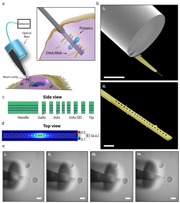
The overall device structure consists of a semiconductor membrane epoxy bonded to the edge of a multimode optical fiber as shown in Figures 1a–b. Nanobeam templates were fabricated out of a thin (220 nm) membrane of gallium arsenide containing three layers of high-density indium arsenide quantum dots (see Methods and Fig. 1c). We choose a standard five-hole taper defect nanobeam22 as our cavity which supports a theoretical fundamental mode Q of 95,000 (Fig. 1d). The width of our beams ranged from 400 – 650 nm, dictated by the wavelength of the cavity modes which center around 1,300 nm (the peak gain of the QD ensemble). Templates were 200–300 μm long and narrowed down to the shown beams at the tip. Fiber tip edges were coated in epoxy and then pressed against a template handle section to rip away the entire membrane (see Supplementary Fig. S1).
Figure 1.
Photonic nanoprobe design and single cell interrogation. a, Schematic of photonic crystal nanobeam probe for single-cell investigation. The nanobeam cavity extends from a larger semiconductor template which is mounted on the side edge of a multimode optical fiber. The inset corresponds to the box in the main figure depicting potential sensing modalities of the cavity such as label-free protein or DNA/RNA detection. b, Angled scanning electron microscope (SEM) pictures of a typical fabricated device (in false-color). The ripple on the fiber facet is a small fracture from the fiber cleaver. A close-up of the beam portion is shown in b(ii). Some light debris from the sputter coating is also visible. The striations on the side of the beam are the three wetting layers of the self-assembled quantum dots. c, Schematic of the MBE material stack. The background material is GaAs and the quantum dots (shown as triangles) are InAs inside an InAs wetting layer. d, Finite-difference time domain simulation picture of the electric field magnitude of the fundamental cavity mode for this photonic structure. e, Sequence of bright-field images of a nanocavity probe penetrating a single PC3 cell, viewed from above. The probe is first positioned outside the cell with the membrane flexed and flush against the petri dish substrate. It is then maneuvered into the side of the cell and finally retracted. The optical fiber, which is positioned higher than the membrane is seen defocused in the pictures. Scale bars: 50 μm (b(i)), 1 μm (b(ii)), 20 μm (e).
Once constructed, the probes can be mounted to a three-axis micropositioner for careful insertion of nanobeams into biological cells. Figure 1e shows a top down optical micrograph sequence of a nanobeam probing a single PC3 cell, a common human prostate cancer cell line24. We probe these cells by lowering the height of our device until the GaAs membrane flexes and flattens onto the petri dish surface (see Supplementary Note II). This way we know that the cavity is lying flush against the substrate and will not slide over the top of a cell. As the cell gets poked by the beam, it elastically deforms upon insertion and retraction, but the overall cell morphology remains unchanged (see Supplementary Video S1).
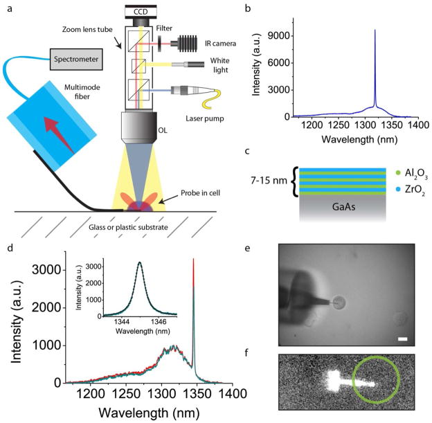
Having demonstrated that we can insert our nanocavities into live PC3 cancer cells in culture, we next investigate their optical properties. Our testing setup is shown in Figure 2a, and consists of a custom built upright zoom lens with multiple ports for laser pumping and image capture (see Methods). Figure 2b shows a spectrum of a cavity in air prior to cell insertion, showing the fundamental mode resonance at 1,319 nm with a Q factor of 1,900, limited by fabrication imperfections (see Supplementary Note I). Naïve insertion of GaAs in an aqueous solution causes destructive photo-induced oxidation, quickly removing any cavity resonance (see Supplementary Figs. S3, S4). We therefore developed a zirconia/alumina nanolaminate protective coating (Fig. 2c) for our devices which serves as a diffusion barrier to oxidants25 (the device in Fig. 2b has the coating already). Figure 2d displays the nanocavity spectra when the probe is placed in a single cell, showing for the first time an active optical resonator in such a biological environment. The cavity peak is now at 1,345 nm and aside from a large redshift (26 nm) from the greater refractive index environment of the cell, we see that the cavity mode persists and actually increased in Q value to 2,000, likely due to reduced absorption by QDs at longer wavelengths. Corresponding optical and IR pictures of the cavity and cell are seen in Figure 2e–f.
Figure 2.
Optical characterization of photonic crystal cavities inside single cells. a, Diagram of the optical setup used in the experiment. A three-axis micromanipulator positions the probe such that the GaAs membrane (shown in black) flexes and rests against the substrate. A zoom lens tube contains beam splitters for laser pump and white light illumination, as well as image capture. OL is objective lens. Not shown is the liquid level, which submerges the optical fiber but does not reach the objective lens. b, PL spectrum of a single nanoprobe cavity measured in air. The QD emission uncoupled to the cavity is the small background spreading from 1,150 nm to 1,350 nm and the cavity mode is the sharp peak at 1,319 nm. c, Illustration of the alumina/zirconia nanolaminate used to coat the entire device, protecting it from photo-induced oxidation. Stacks alternated between 1 nm and 2 nm per layer thicknesses, and total stack thicknesses of 7–15 nm. d, PL spectrum of the same cavity from b now in a cell (teal) and its surrounding medium (red). There is negligible wavelength difference between the two spectra; however the collection intensity inside the cell (teal) is slightly lower, likely due to scattering from the plasma membrane. Inset shows a close-up of the cavity mode which has a Q-factor of 2,200. e, Corresponding white light image of the probe and cell for which data in d were taken. f, Corresponding IR image of the probe’s QD emission and a circular outline of the approximate cell location. Scale bar, 20 μm.
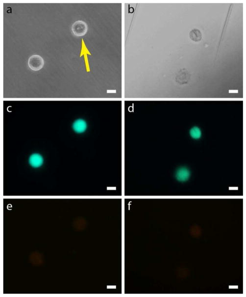
To assess the short-term viability of our PC3 cells after probing we use a standard fluorometric assay of calcein AM and ethidium homodimer, which produces a green fluorescence for cells with live esterase activity and a red fluorescence for cells with compromised plasma membranes (see Methods)26. We find that 75% of cells probed by nanobeams are viable (n = 20) with similar fluorescence intensities as non-probed cells (Fig. 3). In addition to poking cells, we have developed a method to ‘load’ cells with entire beam subunits which are cleaved from the original template handle (see Supplementary Figure S7). Even under such extraordinary conditions we find that the cells can remain viable as seen in Figure 3.
Figure 3.
Short-term cell viability results. a, Phase contrast image of two cells, one of which was poked by a nanoprobe (shown by the arrow) and one which was left untouched. b, Bright field image of two different cells, one which was loaded with a nanobeam and one which was left untouched. The nanobeam is the clear dark line in the upper cell. The cells look different compared to a because the microscope settings were changed to better visualize the cell interior. Also, the two parallel streaks are reference marks scratched into the petri dish with a metal probe to locate the treated cell. c, d, Green fluorescence from the calcein viability dye for the corresponding cells pictured in a and b. All cells show similar levels of green fluorescence intensity indicating the viability of both poked and loaded cells. In d it is even possible to see the outline of the loaded beam in the cell by an absence of color. e, f, Red fluorescence from the ethidium homodimer viability dye for the corresponding cells picture in a and b. The emission is very weak and uniform across all cells indicating the cell membranes were not compromised. Scale bars, 20 μm.
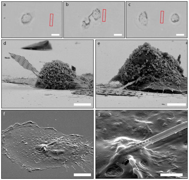
Inspired by the short-term survival of cells with internalized nanobeams, we perform a long-term study by constantly monitoring loaded cells over the course of one week (see Supplementary Note VI). We find that cells not only survive over this time period, but can perform normal cellular functions such as migration and division. Figures 4a–c show microscope images of a loaded cell prior to, during, and after cell division. Miraculously, the nanobeam is passed on to a daughter cell and the two subsequent cells continue to grow and divide. The implications of this result extend beyond this study and show that mesoscopic probes, photonic or otherwise, can potentially be incorporated in cells for monitoring intracellular activity over a long period of time, providing sensor feedback or sending control signals. Future investigations on how these foreign bodies perturb cell gene expression or proteomics will be necessary to identify any subtle changes in cell activity. Figures 4d–g show SEM pictures of fixed cells with nanobeams lodged partially in their interiors, highlighting the penetration of the beams.
Figure 4.
Nanobeam cell division and SEM images of loaded cells. a–c, Bright field images of a loaded cell prior (a), during (b), and after (c) cell division. Images were taken 30, 42, and 46 hours after loading the cell with the nanobeam, respectively. The red box indicated the position of the original scratch mark created during beam loading. This provides a reference mark for seeing how far the cells have migrated, which we observed to be up to 250 μm during the tracking period. d, SEM image of a nanobeam probe including part of the handle tip lodged inside a typical cell. A few flatter cells are seen in the background. e, SEM image of another cell pierced by a nanobeam with connected handle tip. f, SEM image of a cell that has only a beam inserted. This cell was not critical point dried and therefore is much flatter than the cells in d–e. g, Close-up of the entry point of the nanobeam into the cell in f. The holes that make up the cavity are clearly seen as they transition from fully visible outside of the cell to being hidden under the cell membrane. Scale bars: 20 μm (a–c), 5 μm (d–e), 10 μm (f), 2 μm (g).
Finally, we present in vitro protein sensing results for the well-studied system of Streptavidin (SA) -biotin binding using our nanoprobes. It turns out that for repeat measurements in solution the original probe design fails because the GaAs membrane gets folded onto the fiber facet (see Supplementary Section V). We therefore developed a second probe design which consists of ‘wings’ that extend from the main arm and curl around the optical fiber, thus providing structural rigidity and resistance to bending (Figure 5a). For our surface functionalization chemistry, we begin by depositing 2 nm of silica on top of our original nanolaminate using atomic layer deposition (ALD), and then proceed with the standard sequence of aminosilanization, biotinylation, and protein adsorption (Figure 5b)27,19. From the simulation results in Figure 5c we expect a mostly linear response of wavelength redshift with increasing coating thickness, typical of other photonic cavities. Figures 5d–e show the cavity signals for specific and non-specific (biotinylation was skipped) binding for nanobeam cavities attached to a chip substrate. As expected we see a large wavelength shift of 2.9 nm for the specific binding case and a much smaller 0.5 nm redshift for the non-specific binding scenario. We then apply our chemistry and sensing experiment to probe devices (as in Fig. 5a) that were individually placed in beakers and find similar results as shown in Figure 5f. Much like the case with our planar chip cavities, we find a large (3.6 nm) redshift of the probe cavity upon Streptavidin binding. Therefore we have shown that our nanoprobes can be used to detect proteins remotely through optical readout. By adapting the chemistry and combining the method of cellular insertion it will now be possible to perform many kinds of label-free sensing experiments inside living cells.
Figure 5.
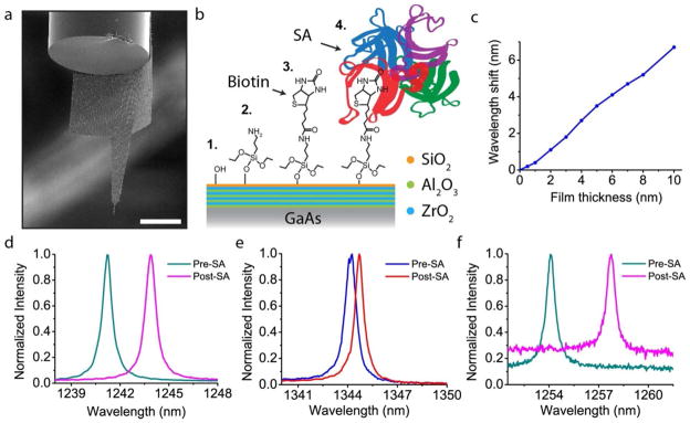
Nanoprobe detection of Streptavidin binding. a, SEM image of a modified nanoprobe that has extended ‘wings’ meant to wrap around the edge of the optical fiber, thus preventing sticking. b, Illustration of the surface chemistry for protein detection. The original, nanolaminate-coated GaAs, is coated with an additional layer of silica which has terminal hydroxyl groups. Aminosilanization with APTES yields an amine-terminated surface to which biotin binds. Finally Streptavidin specifically binds to the surface biotin molecules. c, Finite-difference frequency domain (FDFD) simulation of the expected wavelength shift as the organic film thickness is increased. The film was modeled as a uniform layer of refractive index equal to 1.45. d, Spectra of a chip-bound nanobeam both before and after SA adsorption, demonstrating a clear and large redshift of the cavity peak. e, Non-specific binding of a different beam cavity shows a much smaller redshift of 0.5 nm. f, Spectra of a nanoprobe device (shown in 5a) for the same specific binding chemistry. As in d, the redshift is clear and large. The difference in background PL is due to slightly different focus conditions of the laser spot, however, this has no bearing on the wavelength information. Scale bar, 50 μm.
In conclusion, we have developed a tool which for the first time places a sophisticated photonic resonator inside an individual living cell. Our nanobeam probes are optically sound inside single cells and conversely cells with beams inside them can remain viable and even proliferate long term. We demonstrated protein sensing with our tool as an avenue towards detailed studies of label-free biomarker detection in live, single cells which could shed light on complex cellular processes such as gene expression or drug response. The range of possible applications of this merging between nanophotonics and cell biology is vast and could yield rewarding studies and understandings of fundamental cell biology.
Methods
Fabrication
Wafers were grown by molecular beam epitaxy as described in Ref. 13. The resultant stack consisted of a top layer of 220 nm thick GaAs with three layers of embedded high density (300/μm2) InAs QDs. Below the top GaAs membrane was a 1.5 μm layer of Al0.8Ga0.2As, which was on top of a GaAs substrate. Electron-beam lithography was used to pattern a 300 nm mask of ZEP resist after which the pattern was transferred into the GaAs membrane by dry etching with a BCl3/Cl2 electron-cyclotron resonance reactive ion etch. Structures were then undercut with hydrofluoric acid wet etching. Beams were 20 μm long with the last third of the beam patterned with the air holes that created the optical cavity. The defect cavity had an initial period a = 322 nm linearly tapered down to 266 nm, with hole radius r = 0.22 a. Ten holes created the cavity and an additional five holes were patterned on each side of the cavity for a total of 20 holes.
Atomic layer deposition
All depositions were performed at 200 °C in a Cambridge Nanotech Fiji ALD system. For ZrO2 alternating pulses of tetrakis(dimethylamido)zirconium (TDMA-Zr) and water were used to deposit ZrO2 at 0.8 A/cycle. For Al2O3 alternating pulses of trimethylaluminum (TMA) and water were used to deposit Al2O3 at 1.0 A/cycle. For SiO2 a pulse of tris(dimethylamino)silane (3DMAS) was alternated with a remote O2 plasma to deposit SiO2 at 0.7 A/cycle. A nanolaminate of Al2O3 and ZrO2 was formed by depositing either 1 nm or 2 nm of each film in sequence and repeating this process until the desired thickness was reached.
Device assembly
The experimental procedure is described in the Supplementary Information.
Optics Testing
Samples were tested either in a horizontal microphotoluminescence setup or in an upright custom built zoom lens setup. The horizontal setup consisted of a free-space path for optical pumping of the sample and collection into a spectrometer. A thermoelectric cooled and stabilized laser diode (LD) operating in continuous wave mode at 830 nm was directed through a 100× 0.5 numerical aperture (NA) objective lens onto the sample. PL was collected by the same objective and detected by a liquid nitrogen cooled InGaAs charge-coupled device (CCD) inside a spectrometer. The upright setup consisted of a high magnification zoom lens (Navitar) with a laser injection port and a 20× 0.4 NA objective lens. PL was collected through a 62.5 μm /125 μm core/cladding graded index fiber that was the handle to the nanoprobe. Illumination and laser pump were directed through the objective and through the cell medium onto the specimen. The nanoprobe cavity tested in air was pumped with 150 μW of laser power through the horizontal setup. The same nanoprobe cavity tested in cells and cell medium was pumped with 450 μW of laser power through the upright setup. For protein detection, we use a lower pump power of 50 μW to ensure minimal device heating. Both chip-bound nanobeams and probe nanobeams were measured using the horizontal setup both before and after the surface chemistry.
Simulation
Both FDTD and FDFD simulations were carried out on in-house custom code optimized for photonic structures.
Cell culture and handling
PC3 cells were grown in FK-12 nutrient mixture supplemented with 10% FBS and 1% penicillin/streptomycin. PC3 cells were plated at low density (several thousand cells per 10 cm gridded petri dish) and incubated at 37 °C. Optics and loading experiments were performed on cells in an ambient environment for no more than 2 hours before returning samples to incubation.
Cell viability
A fluorometric assay of calcein AM and ethidium homodimer was used as per the suggested protocol (Invitrogen LIVE/DEAD). Cells were probed or loaded and the positions of those cells were documented by carving out reference marks in the petri dish using a sharp tungsten probe tip. The cells were then incubated for four hours, after which they were treated with 4 μM of calcein AM and 4 μM of ethidium homodimer. Fluorescence images were captured with a Zeiss Axiovert 25 fluorescence microscope with an X-cite mercury lamp source.
SEM imaging
Cells to be imaged were first fixed in 2% glutaraldehyde with 4% paraformaldehyde in 0.1 M Na Cacodylate buffer. We do not apply the typical lipid fixative of OsO4 as we have found out that this chemical corrodes the GaAs semiconductor. Cells were then dehydrated in ethanol and either hexamethyldisilazane (HMDS) or critical point drying. Finally, cells were sputter coated with Au/Pd. Fiber probes were just coated in Au/Pd prior to imaging.
Surface chemistry
Reagents were purchased stock from Sigma Aldrich. Water used was ultrapure 18.2 MΩ reverse osmosis filtered. All glassware was cleaned in multiple washings in acetone, methanol, and water. Experimental chips were first cleaned in acetone, methanol, and water and then blow-dried in an argon stream. For the aminosilanization step, a solution of 2% 3-aminopropyltriethoxy silane (APTES) in anhydrous toluene was prepared. Samples were placed in this solution for 1.5–2 hours and then rinsed with fresh toluene, acetone, methanol, and water followed by argon blow drying. Biotinylation was performed by placing samples in a 4 mg/mL solution of N-hydroxysuccinimide-biotin ester in water for 1 hour, and then rinsed copiously in fresh water followed by argon blow drying. For Streptavidin adsorption, a solution of 100 μg/mL of Streptavidin (from Streptomyces avidinii) in phosphate buffered saline (PBS) was made. Samples were placed in this mixture for 40 minutes and then washed with fresh PBS and water followed by argon blow drying. Chemistry performed on fiber-mounted nanoprobes was exactly the same with the exception of there being no blow drying steps which could potentially break the probes. Fibers were manually inverted, mounted, and held in the various solutions for the described time periods.
Supplementary Material
Acknowledgments
Funding Sources
G. S. was supported by the Stanford Graduate Fellowship. S. R. K. was supported by the Hamalainen Pelican Postdoctoral Fellowship from The Sir Peter and Lady Michael Foundation. Partial funding support was from the Canary Foundation and the NCI ICMIC P50 CA114747 (SSG) CCNE-T U54CA151459 (SSG) and the Beckman Center for Molecular and Genetic Medicine at Stanford University. Work was performed in part at the Stanford Nanofabrication Facility of NNIN supported by the National Science Foundation.
We would also like to acknowledge Molly Lowndes, Jesse Lu, and Lydia-Marie Joubert for helpful discussions.
Footnotes
Author Contributions
G. S., S. R. K., S. S. G., and J. V. conceived and designed the experiments. T. S. and J. H. performed the molecular beam epitaxy growth of the samples. G. S. fabricated and assembled all devices. J P. and G. S. performed ALD on device structures. S. R. K. cultured the cells. G. S. performed all cell probing, optical testing, imaging, and characterization. G. S. and S. R. K. tested cell viability. G. S. developed and applied the surface chemistry and protein detection. G. S. analyzed the data and wrote the manuscript. All authors contributed to discussion and editing of the manuscript.
Supplementary Figure 1: Illustration of device assembly. Supplementary Figure 2: SEM pictures of constructed probe devices. Supplementary Figure 3: Details of cell probing and beam flexibility. Supplementary Video 1: Live insertion of a photonic crystal cavity inside a single PC3 cell. Supplementary Figure 4: Laser induced photo-oxidation of GaAs in water. Supplementary Figure 5: Laser oxidation of cavity inside a cell. Supplementary Figure 6: Control samples for cell viability. Supplementary Figure 7: Process of loading cells. Supplementary Figure 8: Tracking loaded cells. Supplementary Figure 9: SEM pictures of loaded and normal cells. Supplementary Figure 10: SEM pictures of a stuck bayonet-type nanoprobe device. Supplementary Figure 11: Organic layer film thicknesses. Supplementary Figure 12: Label-free sensing for many devices. This material is available free of charge via the Internet at http://pubs.acs.org.
References
- 1.Xie C, Lin Z, Hanson L, Cui Y, Cui B. Nature Nanotech. 2012;7:185–190. doi: 10.1038/nnano.2012.8. [DOI] [PMC free article] [PubMed] [Google Scholar]
- 2.Duan X, et al. Nature Nanotech. 2011;7:174–179. doi: 10.1038/nnano.2011.223. [DOI] [PMC free article] [PubMed] [Google Scholar]
- 3.Singhal R, et al. Nature Nanotech. 2011;6:57–64. doi: 10.1038/nnano.2010.241. [DOI] [PubMed] [Google Scholar]
- 4.Yum K, Na S, Xiang Y, Wang N, Yu M-F. Nano Lett. 2009;9:2193–2198. doi: 10.1021/nl901047u. [DOI] [PMC free article] [PubMed] [Google Scholar]
- 5.VanDersarl JJ, Xu AM, Melosh NA. Nano Lett. 2012;12:3881–3886. doi: 10.1021/nl204051v. [DOI] [PubMed] [Google Scholar]
- 6.Shalek AK, et al. Proc Natl Acad Sci USA. 2010;107:1870–1875. doi: 10.1073/pnas.0909350107. [DOI] [PMC free article] [PubMed] [Google Scholar]
- 7.Robinson JT, et al. Nature Nanotech. 2012;7:180–184. doi: 10.1038/nnano.2011.249. [DOI] [PMC free article] [PubMed] [Google Scholar]
- 8.Hallstrom W, et al. Nano Lett. 2007;7:2960–2965. doi: 10.1021/nl070728e. [DOI] [PubMed] [Google Scholar]
- 9.Yan R, et al. Nature Nanotech. 2012;7:191–196. doi: 10.1038/nnano.2011.226. [DOI] [Google Scholar]
- 10.Tan W, Shi Z-Y, Smith S, Birnbaum D, Kopelman R. Science. 1992;258:778–781. doi: 10.1126/science.1439785. [DOI] [PubMed] [Google Scholar]
- 11.Akahane Y, Asano T, Song B-S, Noda S. Nature. 2003;425:944–947. doi: 10.1038/nature02063. [DOI] [PubMed] [Google Scholar]
- 12.Song B-S, Noda S, Asano T, Akahane Y. Nat Mater. 2005;4:207–210. doi: 10.1038/nmat1320. [DOI] [Google Scholar]
- 13.Ellis B, et al. Nature Photon. 2011;5:297–300. doi: 10.1038/nphoton.2011.51. [DOI] [Google Scholar]
- 14.Corcoran B, et al. Nature Photon. 2009;3:206–210. doi: 10.1038/nphoton.2009.28. [DOI] [Google Scholar]
- 15.Englund D, et al. Nature. 2007;450:857–861. doi: 10.1038/nature06234. [DOI] [PubMed] [Google Scholar]
- 16.Eichenfield M, Chan J, Camacho RM, Vahala KJ, Painter O. Nature. 2009;462:78–82. doi: 10.1038/nature08524. [DOI] [PubMed] [Google Scholar]
- 17.Lee M, Fauchet PM. Opt Express. 2007;15:4530–4535. doi: 10.1364/OE.15.004530. [DOI] [PubMed] [Google Scholar]
- 18.Kita S, et al. Opt Express. 2011;19:17683–17690. doi: 10.1364/OE.19.017683. [DOI] [PubMed] [Google Scholar]
- 19.Scullion MG, Di Falco A, Krauss TF. Biosns Bioelectron. 2011;27:101–105. doi: 10.1016/j.bios.2011.06.023. [DOI] [PubMed] [Google Scholar]
- 20.Shambat G, et al. Appl Phys Lett. 2011;99:191102. doi: 10.1063/1.3660278. [DOI] [Google Scholar]
- 21.Shambat G, et al. Appl Phys Lett. 2012;100:213702. doi: 10.1063/1.4719520. [DOI] [Google Scholar]
- 22.Deotare PB, McCutcheon MW, Frank IW, Khan M, Loncar M. Appl Phys Lett. 2009;94:121106. doi: 10.1063/1.3107263. [DOI] [Google Scholar]
- 23.Vuckovic J, Fattal D, Santori C, Solomon G, Yamamoto Y. Appl Phys Lett. 2003;82:3596–3598. doi: 10.1063/1.1577828. [DOI] [Google Scholar]
- 24.Kaighn ME, Narayan KS, Ohnuki Y, Lechner JF, Jones LW. Invest Urol. 1979;17:16–23. [PubMed] [Google Scholar]
- 25.Meyer J, et al. Adv Mater. 2009;21:1845–1849. doi: 10.1002/adma.200803440. [DOI] [Google Scholar]
- 26.Papadopoulos NG, et al. J Immunol Methods. 1994;177:101–111. doi: 10.1016/0022-1759(94)90147-3. [DOI] [PubMed] [Google Scholar]
- 27.Lapin NA, Chabal YJ. J Phys Chem B. 2009;113:8776–8783. doi: 10.1021/jp809096m. [DOI] [PMC free article] [PubMed] [Google Scholar]
Associated Data
This section collects any data citations, data availability statements, or supplementary materials included in this article.


