Abstract
We present a theory of perfect absorption in a bilayer model composed of a mu-near-zero (MNZ) metamaterial (MM) absorbing layer on a metallic substrate. Our analytical solutions reveal that a MM layer with a large purely imaginary permeability and a moderate permittivity backed by a metallic plane has a zero reflection at normal incidence when the thickness is ultrathin. The impedance-mismatched metamaterial absorber (MA) can be 77.3% thinner than conventional impedance-matched MAs with the same material loss in order to get the same absorption. A microwave absorber using double-layered spiral MMs with a thickness of only about one percent of the operating wavelength is designed and realized. An absorption efficiency above 93% at 1.74 GHz is demonstrated experimentally at illumination angles up to 60 degrees. Our absorber is 98% lighter than traditional microwave absorbers made of natural materials working at the same frequencies.
An electromagnetic absorber is a device which can efficiently absorb incident radiation with negligible reflection and transmission. Conventional electromagnetic absorbers are usually electrically thick. For example, both Salisbury absorber1 and Dällenbach absorber2 have a thickness of quarter wavelength. By using materials having magnetic losses such as ferrites and carbonyl iron1,2, much thinner absorbers can be fabricated. However, these absorbers are heavy due to the high concentrations of iron. In the past few years, a large number of thin absorbers based on high-impedance surfaces (HIS's) have been presented3,4,5,6,7. HIS structures allow achieving absorption by exploiting either resistive losses or intrinsic dielectric loss of the substrate. The above absorbers were limited to microwave and lower frequencies.
In recent years, there have been considerable interests in improving the performance of absorbers using metamaterials (MMs)8,9,10,11,12,13,14,15,16,17,18,19,20,21,22,23,24. MMs allow for the explicit design of almost arbitrary effective permeabilities and/or permittivities, which have greatly extended the designs of metamaterial absorber (MA) from microwave to optical frequencies and for large incidence angles9,10,11. Recently, ε-near-zero/μ-near-zero (ENZ/MNZ) metamaterials, of which Real(ε)/Real(μ) is vanishingly small, have attracted much attention due to many abnormal phenomena25,26,27,28,29,30. Jin et al. predicted perfect absorption could be achieved by some arbitrarily thin ENZs and MNZs with low loss31. Feng et al. also demonstrated perfect absorption (PA) in ultra-thin anisotropic ENZ metamaterials32. The exotic phenomenon was explained by coherent perfect absorption via critical coupling to a fast wave propagating along the ENZ layer. The requirement of low loss ENZs make the realization difficult. Perfect absorption occurs only at a specific oblique angle, which also constrains their applications.
In this work, an ultrathin and lightweight perfect absorber based on mu-near-zero metamaterials is demonstrated. Different from the previous work31,32, the permeability of the metamaterial in our absorber has a vanishing real part but a large imaginary part. Our absorber is superior to the previous absorber design31,32 in that perfect absorption can occur at normal incidence. Analytical formula is developed to calculate the absorption spectrum.
Guided by the analytical formula and MM design process, an ultrathin MA using mu-near-zero MMs is designed and fabricated. Our experiment shows an absorption over 93% at incidence angles up to 60°, which agrees well with both the analytical and simulation results. Our sample has an electrical thickness of about only λ/90 and is 98% lighter than traditional microwave absorbers made of natural materials working at the same frequencies, which shows great advantages in many defense and civil applications.
It is important to note that the MA design concept we addressed here is different from the previous MAs in Refs. 8,11,13 and 22. In these previous works, the whole MAs are characterized by complex effective medium parameters ε and μ and the essential idea is to form an impedance-matched (ε = μ) lossy layer. Recently, Chen claimed that such a MA can hardly be considered as an effective bulk medium due to its strong inhomogeneity in the wave propagating direction24. However, such a problem does not exist in our design, wherein only the MM layer on the top of the PEC plane is characterized by ε and μ. With the present idea, various metamaterial absorbers can be designed flexibly by standard MM design process.
Results
Theoretical approach
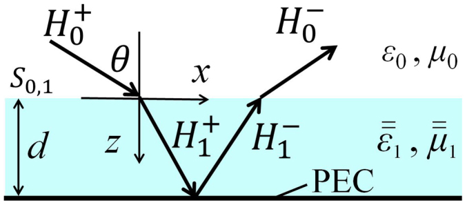
Figure 1 illustrates the structure for achieving perfect absorption. A metamaterial slab with a thickness d is sandwiched between a semi-infinite layer and the bottom backing perfect electric conductor (PEC). The top layer and the slab are denoted as regions 0 and 1, respectively. For simplicity, assuming region 0 to be the free space with permittivity ε0 and permeability μ0. The relative permittivity and permeability tensors of the metamaterial in region 1 can be described by  and
and  , respectively. A transverse magnetic (TM) plane wave impinges on the metamaterial slab with incident angle θ (the magnetic field is along the y axis). Assuming a harmonic time dependence exp(−iωt) for the EM field, from Maxwell's equations, the magnetic and electric fields in layer n can be expressed as31
 |
where Hn± is the magnetic field amplitude of a down- or up-going plane wave component in layer n,  ,
,  ,
,  ,
,  , and
, and  . By applying boundary conditions at the interfaces (the continuities of the tangential components of the magnetic and electric field across the surface S0,1 and the zero-tangential component of the electric field on the PEC boundary condition), one can obtain Hn± and the corresponding field distributions in region n. The reflection coefficient is
Since the transmission T is zero, the absorption is related to reflection as  , so perfect absorption (PA) is achieved if reflection r = 0. To get a simplified solution for μ1y
, we can take the approximation
  when
when  . Then we obtain
For the normal incidence case (θ = 0°), Eq. (3) reduces to
Then the solution for the PA condition is  where λ is the wavelength in free space. Substitution of the PA condition into approximation condition
  yields
  . From the above discussions, two main conditions are required to get PA at normal incidence. Firstly, the thickness d and the permittivity ε1x must be small enough to meet the approximation condition
  , and secondly μ1y must equal
  , which is purely imaginary and inversely proportional to thickness d.
Figure 1. Configuration of the theoretical model for TM polarization.
Thickness and loss dependence
Here we use  and
and  (in unit of dB) to represent more clearly the reflection and transmission, respectively. As clearly shown in Eq. (2), the reflection is determined by permeability μ1y, thickness d, permittivity ε1x and ε1z. For simplicity, the permittivity is assumed to have a moderate normal value, for example, ε1x = ε1z = 1. The angular reflections are plotted in Fig. 2 for MAs with thickness d = λ/90, which are calculated using the exact formula (2) for five cases of μ1y. Figure 2a shows the angular reflection of our MM absorber with purely imaginary μ1y of five representative values, namely, (1i, 9i, 14.3i, 20i, 50i). It is found that the reflection at normal incidence is minimized (−38 dB, i.e. 99.984% absorption) when
  , which is in agreement with Eq. (4). It is also noted that the maximized absorption will occur at a nonzero incident angle if imag(μ1y) of the MM is smaller than 14.3 (a smaller imaginary part of μ1y will give a smaller absorption).
Figure 2. Angular reflection performance of different MAs with thickness d = λ/90.
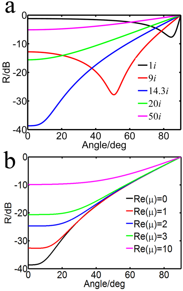
(a) (ε1x, μ1y) has values of (1, 1i), (1, 9i), (1, 14.3i), (1, 20i) and (1, 50i) for black, red, blue, green, magenta lines, respectively. (b) (ε1x, μ1y) has values of (1, 14.3i), (1, 1 + 14.3i), (1, 2 + 14.3i), (1, 3 + 14.3i) and (1, 10 + 14.3i) for black, red, blue, green, magenta lines, respectively.
Figure 2b plots the angular reflections for different values of real(μ1y) [with imag(μ1y) = 14.3 fixed]. It is found that any deviation of real(μ1y) from zero would cause higher reflection (i.e., lower absorption) for all the incident angles. Thus, it is critical to maintain a vanishing real part of μ1y to achieve large absorption.
Figure 3a plots the angular reflection of the MA for different values of thickness d with (ε1x, μ1y) = (1, 14.3i). For the thinnest case of d = λ/1000, the lowest reflection occurs at a large oblique angle, and the angle approaches to 0 (the normal incidence) as d increases. However, when the thickness increases beyond λ/90, the reflection rises up, implying lower absorption. Figure 3b shows the reflections for five cases with different values of slab thickness d and different values of permeability. The product of d and μ1y is fixed to  to fulfill the conditions of perfect absorption at normal incidence. Interestingly, the highest absorption is obtained for the thinnest case. These figures demonstrate that an extremely sub-wavelength MM with a large purely imaginary μ is critical to get PA.
Figure 3. Angular reflection performance of different MAs.
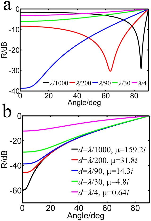
(a) (ε1x, μ1y) = (1, 14.3i), thickness d is λ/1000, λ/200, λ/90, λ/30, λ/4 for black, red, blue, green, magenta lines, respectively. (b) (d, ε1x, μ1y) has different values of (λ/1000, 1, 159.2i), (λ/200, 1, 31.8i), (λ/90, 1, 14.3i), (λ/30, 1, 4.8i) and (λ/4, 1, 0.64i) with  fixed for black, red, blue, green, magenta lines, respectively.
The role of the PEC plane
One may want to know what will happen if the PEC plane is removed. Without PEC plane, the transmission cannot be neglected. The reflection and transmission coefficients are given by33,34
where  , and
, and  .
.
The reflection and transmission for the cases of (1, 14.3i) without PEC are plotted in Fig. 4 according to Eq. (5a) and (5b) by the red solid and dotted curves, respectively. Both the reflection and transmission increase when PEC is removed. We can conclude that the PEC plane not only block the transmission, but also plays an important role in reducing the reflection. It can be understood by destructive interference as mentioned in Ref. 31. When the incident wave impinges on surface S0,1, there will be a direct reflection component p0 due to the impedance-mismatch. The wave which enters the slab is multi-reflected by surface S0,1 and the PEC plane and repeatedly absorbed, and a part of it, denoted by component p1, is multi-refracted out of surface S0,1. Due to the unique property of MNZ layer and an appropriate thickness, component p1 is 180 degrees out of phase with component p0 and thus results in destructive interference.
Figure 4. (d, ε1x, μ1y) has the values of (λ/90, 1, 14.3i).
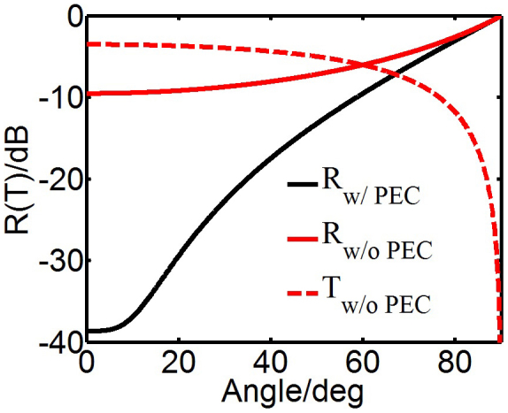
The black line is the reflection of the MA. The red solid and dotted lines are the reflection and transmission, respectively, when the PEC plane is removed from the MA.
Comparison with the conventional idea of MAs
In previous MAs8,19, the essential idea is to design a highly lossy meta-structure with an intrinsic impedance matched with free space, i.e. ε1 = μ1. The complex index of refraction is  . For the normal incidence case, Eq. (5a) and (5b) reduce to r = 0 and
  . Although the reflection vanishes due to impedance-match, the transmission cannot be neglected, which is given by
  (dB). When the MM has the same loss as our impedance-mismatched case, for instance,
  , to achieve the same absorption level (−38 dB) the thickness d of the MA is required to be λ/20.5, implying that our design (λ/90) can be 77.3% thinner than previous impedance-matched MA designs. The above discussions show that our impedance-mismatched case of (1, 14.3i) has great advantages over the conventional impedance-matched case of (14.3i, 14.3i) in thin absorber designs. Furthermore, for practical realization, it is much easier to implement MMs with a single abnormal (zero) parameter.
Experimental realization of an ultrathin MA
According to the above analysis, a MM absorber with ultra-thin thickness can be obtained by employing MM with a large imaginary part of μ1y. Here we utilize double-layered spiral metamaterial35 as shown in Fig. 5a. The second spiral layer on the bottom has 180° rotational symmetry about the z-axis with respect to the top spiral (see Fig. 5a). The 180° rotation symmetry can not only doubles the inductances of the meta-structure due to their arrangement in series35, but also enhances the capacitance C due to the interlayer interaction. The spiral response can be approximated based on a simple LC resonator model  , where ω0 is the resonant angular frequency, L is the inductance and C is the capacitance of the MM. So the unit cell size is greatly reduced as a result of the enhanced inductance and capacitance. The two identical spirals with different orientations are spaced by a dielectric substrate made up of Rogers Printed circuit board (PCB). The parameters of the unit cell are as follows: dimensions of unit cell px = 4.1 mm and d = 1.9 mm, strip width w = 0.127 mm, separation between the strips s = 0.127 mm, number of turns N = 3.5. The period py in the y direction is equal to px. Numerical simulations are carried out using a frequency domain solver, implemented by CST Microwave Studio TM 201036 (see Methods below).
Figure 5.
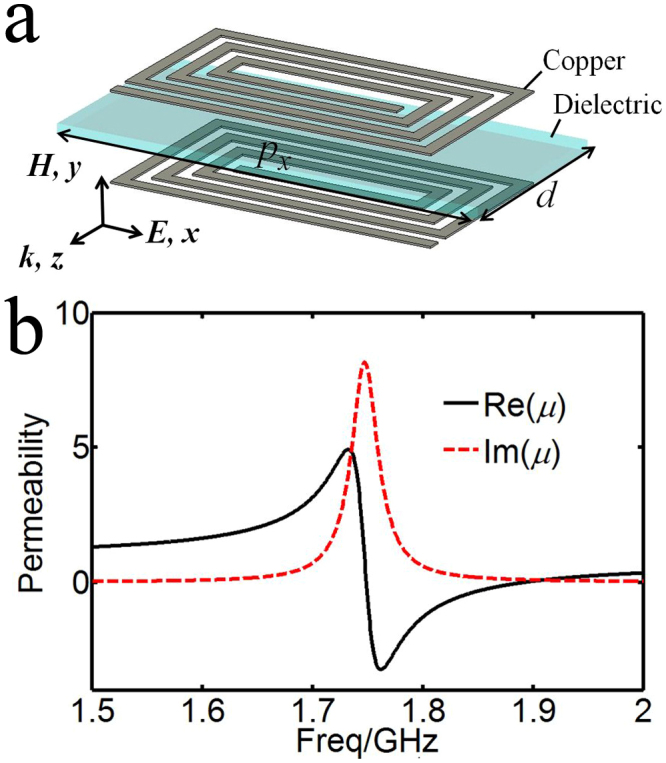
(a) Schematic (exploded view) of the dual-layer square spiral metamaterial.(b) The effective permeability of the unit cell. The black solid line and red dashed line denote real and imaginary parts, respectively.
The effective parameters of the metamaterials slab are retrieved through the transfer-matrix method approach33,34, using the simulated scattering parameters, S11 and S21.The effective permittivity ε1x keeps nearly a constant of 2.87, which is not shown here. The extracted effective permeability is shown in Fig. 5b. The unit cell exhibits a Lorentz-type magnetic response near the resonance frequency 1.745 GHz with μ1y = 8.6i. The electrical thickness d is nearly λ/90 and ε1x is 2.87, which satisfy the approximation condition of  .
.
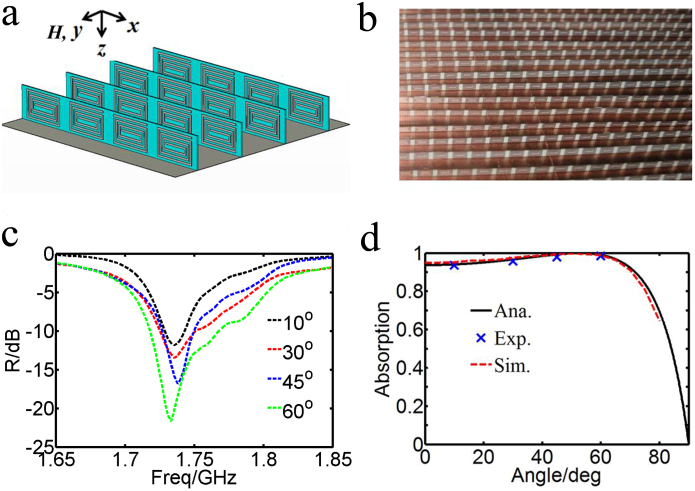
The configuration of our MM absorber structure is shown in Fig. 6a, which is constructed by periodic unit cells with a metal ground plate(see Methods below). The periods in the x and y directions are the same, i.e. px = py. Four incident angles, namely, 10°, 30°, 45° and 60°, are selected. As depicted in Fig. 6c, reflection dips lower than −12 dB at 1.74 GHz for all these incidence angles are observed. The operating frequency deviates slightly from 1.745 GHz in the effective medium model, which is due to the fabrication imperfections. The angular reflection spectrum is minimized at 60°, which agrees with the analytical reflection for the case of (2.87, 8.6i) (see Fig. 6d). The comparison of experimental absorptions at 1.74 GHz with the analytical and simulation results is shown in Fig. 6d. Absorption over 93% at incidence angles up to 60° has been achieved. The experimental results agree well with both the analytical and simulation results, even in the presence of the background noise due to the limited sample size.
Figure 6.
(a) 3D illustration of the MA structure for one polarization (each unit cell is formed by the dual-layer square spiral metamaterial shown in Fig. 5a and a metal film is on the bottom).(b) Photograph of the fabricated sample. (c) the experimental reflection of the MA at 10°, 30°, 45° and 60° incidence angles. (d) the analytical, simulated and experimental angular absorptions of the MA at 1.74 GHz.
Then we measure the thickness and weight of our sample. The overall thickness of the MA is 1.917 mm (λ/90) (take the backing copper film of 17 μm-thick into account) and the evaluated weight density is about 0.18 kg/m2. Our sample is 33% thinner and 98% lighter than traditional microwave absorbers made of natural materials working at the same frequencies38,39. This reveals that our ultrathin and light MA has a promising application potential in military and civil areas where light and thin absorbers are demanded.
As a final remark, since the periods of our MM slab in the x and y directions are carefully designed to be equal, it is easy to obtain a polarization-independent absorber (which is usually the case of radar absorbing applications) by packing them into a 2D isotropic unit cell, as the ones proposed, for instance in Ref. 40.
Discussion
In summary, we have given an analytical model to demonstrate the absorption performance of an anisotropic metamaterial layer on a metal plate. The dependence of the absorption on the thickness and the constitutive parameters of the slab is shown for TM polarized incident wave. Based on the analytical equations, we have designed and fabricated an ultrathin and lightweight absorber using extremely sub-wavelength double-layered spiral MMs with the electrical thickness of only λ/90. Our absorber with a highly lossy MNZ layer can exhibit nearly perfect absorption when incidence angle is smaller than 60°, which is advantageous over impedance-matched MA for practical realization. The benefit of thin and lightweight absorbers, compared with traditional absorbers made of natural materials, brings great potential in many defense and civil applications. This concept can be extended to other frequencies, such as terahertz, infrared and optical frequencies.
Methods
Simulations
In the simulations, all metallic components are modeled as copper with a conductivity of σ = 5.8 × 10⁷ S/m and the dielectric constant and loss tangent of the dielectric spacer are 2.9 and 0.01, respectively. Excitations from waveguide ports are used where the electric field is along the x direction for extracting ε1x, and the magnetic field is along y (see Fig. 5a). In the simulation to get the numerical absorption, a TM wave with the magnetic field polarized along the y direction is chosen as the excitation source (see Fig. 6a). Periodic boundary conditions are set in the x and y directions.
Fabrication and measurements
The MMs are fabricated by using the standard PCB photolithography. Then we cut them into tens of strips and pack up the strips on a PCB with 17 μm copper sheet as shown in Fig. 6a. The copper sheet can act as the PEC plane at the microwaves. All fabricated dimensions are identical to those simulated and the photograph is shown in Fig. 6b. The MA has 50 unit cells in the x direction and 48 strips in the y direction with an area of 205 mm × 196.8 mm. The absorption performance of the tested sample is experimentally verified by measuring the complex S-parameters in a microwave anechoic chamber. The experimental setup is the same as that in Ref. 37. Two horn antennas are connected to a R&S ZVB vector network analyzer as the transmitter and receiver. The measured reflection is normalized with respect to a copper plane with the same dimensions as the sample.
Author Contributions
S.H. initiated the idea and supervised the finding of the present work. S.Z. did the calculation and experiment. S.Z. and S.H. wrote the paper.
Acknowledgments
We acknowledge Zuojia Wang and Prof. Hongsheng Chen from the Electromagnetic Academy at Zhejiang University for their great help in the sample test. Shuomin Zhong would like to thank Yingran He, Fei Ding, Dr. Yi Jin and Prof. Yungui Ma for fruitful discussions. This work is partially supported by the National High Technology Research and Development Program (863 Program) of China (No. 2012AA030402), the National Natural Science Foundation of China (Nos. 61178062 and 60990322), Swedish VR grant (# 621-2011-4620) and AOARD.
References
- Ruck G. T., Barrick D. E. & Stuart W. D. Radar Cross Section Handbook., Plenum, New York (1970).
- Knott E., Shaeffer J. F. & Tuley M. T. Radar Cross Section., 2nd ed., Scitech, Raleigh (2004).
- Engheta N. Thin absorbing screens using metamaterial surfaces. Proc. IEEE 2, 392–395 (2002). [Google Scholar]
- Simms S. & Fusco V. Thin radar absorber using artificial magnetic ground plane. Electron. Lett. 41, 1311–1313 (2005). [Google Scholar]
- Mosallaei H. & Sarabandi K. A one-layer ultra-thin meta-surface absorber. Proc. IEEE 1B, 615–618 (2005). [Google Scholar]
- Gao Q. et al. A novel radar-absorbing-material based on EBG structure. Microw. Opt. Technol. Lett. 47, 228–230 (2005). [Google Scholar]
- Padooru Y. R. et al. Circuit modeling of multiband high-impedance surface absorbers in the microwave regime. Phys. Rev. B 84, 035108 (2011). [Google Scholar]
- Landy N. I., Sajuyigbe S., Mock J. J., Smith D. R. & Padilla W. J. Perfect metamaterial absorber. Phys. Rev. Lett. 100, 207402 (2008). [DOI] [PubMed] [Google Scholar]
- Tao H. et al. Highly flexible wide angle of incidence terahertz metamaterial absorber: Design, fabrication, and characterization. Phys. Rev. B 78, 241103 (2008). [Google Scholar]
- Wang B. et al. Wide-angle and polarization-independent chiral metamaterial absorber. Phys. Rev. B 80, 033108 (2009). [Google Scholar]
- Avitzour Y., Urzhumov Y. A. & Shvets G. Wide-angle infrared absorber based on a negative-index plasmonic metamaterial. Phys. Rev. B 79, 045131 (2009). [Google Scholar]
- Landy N. I. et al. Design, theory, and measurement of a polarization-insensitive absorber for terahertz imaging. Phys. Rev. B 79, 125104 (2009). [Google Scholar]
- Liu X. et al. Infrared spatial and frequency selective metamaterial with near-unity absorbance. Phys. Rev. Lett. 104, 207403 (2010). [DOI] [PubMed] [Google Scholar]
- Ye Y. Q. et al. Omnidirectional, polarization-insensitive and broadband thin absorber in the terahertz regime. J. Opt. Soc. Am. B 27, 498–504 (2010). [Google Scholar]
- Liu N. et al. Infrared perfect absorber and its application as plasmonic sensor. Nano Lett. 10, 2342–2348 (2010). [DOI] [PubMed] [Google Scholar]
- Alici K. B. et al. Experimental verification of metamaterial based subwavelength microwave absorbers. J. Appl. Phys. 108, 083113–083113 (2010). [Google Scholar]
- Ding F., Cui Y., Ge X., Jin Y. & He S. Ultra-broadband microwave metamaterial absorber. Appl. Phys. Lett. 100, 103506–103506 (2012). [Google Scholar]
- Pang Y. et al. Ultrathin and broadband high impedance surface absorbers based on metamaterial substrates. Opt. Express 20, 12515–12520 (2012). [DOI] [PubMed] [Google Scholar]
- Watts C. M., Liu X. & Padilla W. J. Metamaterial Electromagnetic Wave Absorbers. Adv. Mater. 24, OP98 (2012). [DOI] [PubMed] [Google Scholar]
- Tao H. et al. A metamaterial absorber for the terahertz regime: Design, fabrication and characterization. Opt. Express 16, 7181–7188 (2008). [DOI] [PubMed] [Google Scholar]
- Li H. et al. Ultrathin multiband gigahertz metamaterial absorbers. J. Appl. Phys. 110, 014909–014909 (2011). [Google Scholar]
- Hao J., Zhou L. & Qiu M. Nearly total absorption of light and heat generation by plasmonic metamaterials. Phys. Rev. B 83, 165107 (2011). [Google Scholar]
- Meng L., Zhao D., Li Q. & Qiu M. Polarization-sensitive perfect absorbers at near-infrared wavelengths. Opt. Express 21, A111–A122 (2013). [DOI] [PubMed] [Google Scholar]
- Chen H. T. Interference theory of metamaterial perfect absorbers. Opt. Express 20, 7165–7172 (2012). [DOI] [PubMed] [Google Scholar]
- Silveirinha M. et al. Tunneling of electromagnetic energy through subwavelength channels and bends using ε-near-zero materials. Phys. Rev. Lett. 97, 157403 (2006). [DOI] [PubMed] [Google Scholar]
- Alù A. et al. Epsilon-near-zero metamaterials and electromagnetic sources: Tailoring the radiation phase pattern. Phys. Rev. B 75, 155410 (2007). [Google Scholar]
- Ma Y. G. et al. Near-field plane-wave-like beam emitting antenna fabricated by anisotropic metamaterial. Appl. Phys. Lett. 94, 044107–044107 (2009). [Google Scholar]
- Jin Y. & He S. Enhancing and suppressing radiation with some permeability-near-zero structures. Opt. Express 18, 16587–16593 (2010). [DOI] [PubMed] [Google Scholar]
- Huang X. et al. Dirac cones induced by accidental degeneracy in photonic crystals and zero-refractive-index materials. Nat. Mater. 10, 582–586 (2011). [DOI] [PubMed] [Google Scholar]
- Hao J., Yan W. & Qiu M. Super-reflection and cloaking based on zero index metamaterial. Appl. Phys. Lett. 96, 101109–101109 (2010). [Google Scholar]
- Jin Y. et al. Arbitrarily thin metamaterial structure for perfect absorption and giant magnification. Opt. Express 19, 11114–11119 (2011). [DOI] [PubMed] [Google Scholar]
- Feng S. & Halterman K. Coherent perfect absorption in epsilon-near-zero metamaterials. Phys. Rev. B 86, 165103 (2012). [Google Scholar]
- Smith D. R. et al. Determination of effective permittivity and permeability of metamaterials from reflection and transmission coefficients. Phys. Rev. B 65, 195104 (2002). [Google Scholar]
- Chen X. et al. Robust method to retrieve the constitutive effective parameters of metamaterials. Phys. Rev. E 70, 016608 (2004). [DOI] [PubMed] [Google Scholar]
- Chen W. C. et al. Extremely subwavelength planar magnetic metamaterials. Phys. Rev. B 85, 201104 (2012). [Google Scholar]
- CST Studio Suite 2010, CST of America, 2010.
- Huang L. & Chen H. Multi-band and polarization insensitive metamaterial absorber. Prog. Electromagn. Res. 113, 103–110 (2011). [Google Scholar]
- http://www.eccosorb.com/Collateral/Documents/English-US/SF.pdf.
- http://www.eccosorb.com/Collateral/Documents/English-US/FGM.pdf.
- Baena J. D. et al. Electrically small isotropic three-dimensional magnetic resonators for metamaterial design. Appl. Phys. Lett. 88, 134108–134108 (2006). [Google Scholar]


