

Abstract
The quantitative, real time detection of single stranded oligonucleotides with silicon nanowires (SiNWs) in physiologically relevant electrolyte solution is demonstrated. Debye screening of the hybridization event is minimized by utilizing electrostatically adsorbed primary DNA on an amine-terminated NW surface. Two surface functionalization chemistries are compared: an amine terminated siloxane monolayer on the native SiO2 surface of the SiNW, and an amine terminated alkyl monolayer grown directly on a hydrogen-terminated SiNW surface. The SiNWs without the native oxide exhibit improved solution-gated field-effect transistor characteristics and a significantly enhanced sensitivity to single stranded DNA detection, with an accompanying two orders of magnitude improvement in the dynamic range of sensing. A model for the detection of analyte by SiNW sensors is developed and utilized to extract DNA binding kinetic parameters. Those values are directly compared with values obtained by the standard method of surface plasmon resonance (SPR), and demonstrated to be similar. The nanowires, however, are characterized by higher detection sensitivity. The implication is that Si NWs can be utilized to quantitate the solution phase concentration of biomolecules at low concentrations. This work also demonstrates the importance of surface chemistry for optimizing biomolecular sensing with silicon nanowires.
Introduction
Over the past few years a number of new biomolecular sensors have been reported.1–5 The development of these devices is in part driven by the emerging needs of both systems biology6,7 and personalized and predictive medicine8 – both of which are increasingly requiring quantitative, rapid, and multiparameter measurement capabilities on ever smaller amounts of tissues, cells, serum, etc. To meet these needs, many groups have focused their attention on developing real time, highly sensitive and potentially scalable tools for detecting nucleic acids and proteins. One-dimensional nanostructures such as nanotubes,9–11 semiconductor,12,13 metal oxide nanowires (NWs),14 and conducting polymer nanofilaments15 have all been demonstrated as capable of the label-free detection of small molecules, nucleic acids, and proteins.
Silicon nanowire (SiNW) biosensors are promising label-free, electronic-based detectors of biomolecules.2 However, significant scientific challenges remain before SiNW sensors can be viewed as a realistic technology. One challenge relates to the use of these devices in biologically relevant media, which is typically a 0.14M electrolyte. NW sensors detect the local change in charge density (and the accompanying change in local chemical potential) that characterizes a target/capture agent binding event. That changing chemical potential is detected as a ‘gating’ voltage by the NW, and so, at a given voltage, affects the source (S) → drain (D) current value, or ISD. However, that change is screened (via Debye screening) from the NW by the solution in which the sensing takes place.16 Debye screening is a function of electrolyte concentration, and in a 0.14M electrolyte (which represents physiological environments such as serum) the screening length is about 1 nm.17 Because of this, all reports on SiNW sensors for proteins or DNA have been carried out in low ionic strength solutions.12,13,18 In this paper, we demonstrate that a single-stranded complementary oligonucleotide is able to significantly change the conductance of a group of 20 nm diameter SiNWs (p-doped at ~1019 cm−3) in 0.165M solution by hybridizing to a primary DNA strand that has been electrostatically adsorbed onto an amine terminated organic monolayer atop the NWs. This intimate contact of the primary strand with the amine groups of the NW surface brings the binding event close enough to the NW to be electronically detected. In addition, within a 0.165M ionic strength solution the DNA hybridization is more efficient.10,19
A second challenge involves demonstrating reproducible and high-throughput nanofabrication methods that can produce nearly identical NW sensors time and time again, and that allow for multiple measurements to be executed in parallel. Dimensional arguments20 imply that that the fabrication of highly sensitive NW sensors requires non-traditional fabrication methods.21,22 To date, all reports of NW sensors have utilized semiconductor NWs grown as bulk materials23 using the vapor-liquid-solid (VLS) technique.24 This method produces high quality NWs, but they are characterized by a distribution of lengths and diameters, and they also must be assembled into the appropriate device structure (or the device structure must be constructed around the nanowire25). In this paper we utilize the Superlattice Nanowire Pattern Transfer (SNAP) method26 to produce highly aligned array of 400 SiNWs, each 20 nm wide and ~2 millimeters long. Standard nano and microfabrication techniques are utilized to control the NW doping level,27 to section the NWs into several individual sensor arrays, to establish electrical contacts to the NW sensors, and to integrate each array into a microfluidic channel. The resulting NWs exhibit excellent, controllable, and reproducible electrical characteristics from device-to-device and across fabrication runs. The sensor platforms may also be fabricated in reasonably high throughput.
A third challenge involves the SiNW surface. The effectiveness of SiNWs for biomolecular sensing arises in part because of their high surface-to-volume ratio. The native (1–2 nm thick) surface oxide on a SiNW may limit sensor performance due to the presence of interfacial electronic states.28,29 In addition, the oxide surface of SiNWs acts as a dielectric which can screen the NW from the chemical event to be sensed. Covalent alkyl passivation of Si(111) surfaces can render those surfaces resistant to oxidation in air30 and under oxidative potentials.31 Recently, methyl passivated SiNWs were shown to exhibit improved field-effect transistor characteristics.32 More complex molecules, such as amine terminated alkyl groups, can be covalently attached to H-terminated Si surfaces (including SiNWs) via UV-initiated radical chemistry.33–36 Such chemistry has been used for the covalent attachment of DNA to VLS grown SiNWs.37 DNA may also be immobilized on amine-terminated surfaces via electrostatic interactions. In this paper, we explore how the characteristics of SiNW sensors vary as the nature of the inorganic/organic interface is varied. We find that SiNW sensors in which the native oxide provides the interface for organic functionalization are significantly inferior in terms of both sensitivity and dynamic range when compared with SiNW sensors that are directly passivated with an alkyl monolayer.
A final challenge is actually an opportunity that is provided by the intrinsic nature of a label free, real time sensor. The standard such sensing technique is surface plasmon resonance (SPR).38 SPR is utilized to determine the kon and koff rates, and hence the equilibrium binding affinities, of complementary DNA strands, protein-antibody binding, etc. The capture agent (e.g. single stranded DNA) is typically surface-bound, and so the key experimental variables are the analyte (complementary strand) concentration and time. If kon and koff are both known, then SPR can be utilized to quantitate the analyte concentration. Very few biomolecular sensing techniques are quantitative. In this paper we dope the NW sensors so that their sensing dynamic range is optimized to match that of SPR for the detection of DNA hybridization. We demonstrate the equivalence of these two methods, and thus demonstrate the potential use of SiNW sensors for quantitating analyte concentrations. SiNW sensors can be optimized for significantly higher sensitivity than SPR, and thus can potentially be utilized to quantitate the concentrations of specific biomolecules at very low concentrations. That would constitute a unique application of these devices.
Experimental Methods
Si NW fabrication
The Si NW arrays were fabricated as previously described,39 and all fabrication was done within a class 1000 or class 100 clean room environment. A typical NW sensor device employed in this work for DNA sensing is shown in Figure 1. The starting material for the SNAP process was an intrinsic, 320 Å thick silicon-on-insulator (SOI) substrate with (100) orientation (Ibis Technology Inc., Danvers, MA) and with a 1500 Å buried oxide. Cleaned substrates were coated with either p-type (Boron A, Filmtronics, Inc. Bulter, PA) or n-type (Phosphorosilica, Emulsitone, Inc., Whippany, NJ) spin-on-dopants (SODs). SODs were thermally diffused into the SOI film. We reproducibly controlled the resulting substrate doping concentration, as quantified by 4-point resistivity measurements on the SOI film, by varying the diffusion temperature. For this study, a 3 minute, 850°C (875°C) rapid thermal anneal was used to generate p (n) dopant levels of ~8×10¹⁸/cm3. The p-type substrates were thermally oxidized in O2 for 1 minute at 850°C, which was necessary to remove the organic SOD residue. The SOD films were removed by brief immersion in piranha (70% H2SO4, 30% H2O2), followed by a water rinse, and immersion in buffered oxide etchant (BOE; General Chemical, Parcippany, NJ).
Figure 1.

A diagram (A) and an SEM image (B) of a single device section containing three groups of ~10 SiNWs in a microfluidics channel. The wafer is covered with Si3N4 except for an exposed active region with SiNWs (A, inset; B). B, inset: High resolution SEM image of 20 nm SiNWs.
The SNAP method for NW array fabrication translates the atomic control achievable over the individual layer thicknesses within an MBE-grown GaAs/AlxGa(1-x)As superlattice into an identical level of control over NW width, length and spacing. This method has been described in some detail elsewhere,26,39 and will not be described here. We utilized the SNAP process to produce a 2 mm long array of 400 SiNWs, each of 20 nm width and patterned at 35 nm pitch (Fig 1B, inset).
The SiNWs were sectioned into ~30 µm long segments using e-beam lithography (EBL) and SF6 RIE etching, producing segments of ~10 SiNWs, each with a width of 20 nm. Six identical sections, each containing 3 NW segments were produced. One such section is shown in Figure 1. When fully integrated with the microfluidics channels, this allowed for six separate measurements, with three independent NW segments per measurement. Source (S) and drain (D) electrical contacts, ~500 nm wide and separated by 10–15 µm, were patterned using electron beam lithography (EBL) on each section of SiNWs. Prior to metallization, the native oxide of the SiNWs over the contacts was removed with BOE to promote the formation of ohmic contacts. Finally, 400 Å Ti and 500 Å Pt were evaporated to form S/D contacts. Immediately after the lift-off, the devices were annealed in 95% N2, 5% H2 at 475°C for 5 minutes. This step greatly improves the characteristics of SNAP SiNW FETs. To provide room for a 1 cm by 1.5 cm PDMS chip with microchannels for analyte delivery to each section of the SiNWs (Figure 1A), the electrical contacts were extended to the edges of the substrate using standard photolithography techniques followed by evaporation of 200 Å Ti and 1500 Å Au. To eliminate parasitic current between metal contacts in solution, approximately 70 nm of Si3N4 was deposited using plasma-enhanced chemical vapor deposition (PECVD) everywhere on the chip except in 5 µm by 20 μm regions over the NWs and the outer tips of the Au contacts. Briefly, 100 nm of chromium was deposited over an active region of the NWs. PECVD was used to deposit Si3N4 film at 300°C (900mT, 20W, 13.5MHz) from N2 (1960 sccm), NH3 (55 sccm) and SiH4 (40 sccm) gases. The nitride film was selectively etched with CHF3/O2 plasma over the protected NW region using PMMA as a mask, followed by the removal of chromium with CR-7C (Cyantek Corp., Fremont, CA).
Microfluidics Fabrication
The soft lithography microfluidics chips were fabricated as described by others.40 We observed that manual introduction/changing of solutions caused serious noise, capacitive currents and baseline shifts in real-time recordings. Thus, for low noise, stable real-time electronic measurements, we found it necessary to automate fluid injection and solution switching by using PDMS multilayer, integrated elastomeric microfluidics chips of the type developed by the Quake and Scherer groups.41 The size of the wafer containing SiNWs did not permit the inclusion of all necessary flow and control lines necessary for the fluidic handling chip, and so that was fabricated as a separate chip. The Supporting Information of this article contains the details of microfluidics chip fabrication and device assembly.
Synthesis of tert-Butyl allylcarbamate
To a solution of allylamine (2.27 g, 39.8 mmol) in THF (20 ml) was added N,N-diisopropylethylamine (13 ml, 80.0 mmol) followed by di-tert-butyl dicarbonate (8.7 g, 39.9 mmol). After 1 hr, the organic solvent was evaporated under reduced pressure, and the residue was purified by silica gel chromatography (Hex : EtOAc = 9 : 1) to give 6.6 g (93 %) of a product as a clear oil. 1H NMR 300 MHz (CDCl3) δ 5.82 (m, 1H), 5.12 (m, 2H), 3.74 (bm, 2H), 1.45 (s, 9H).
Surface Functionalization
The two procedures used to functionalize SiNWs with and without oxide layer are shown in Schemes 1 and 2, respectively. Both procedures resulted in an amine terminated organic monolayer atop SiNWs. For the oxide surface functionalization, cleaned SiNWs were treated with 2% (v/v) 3-aminopropyldimethylethoxysilane (Gelest, Inc., Morrisville, PA) in toluene for 2 hrs. The wafers were then rinsed in toluene and methanol and incubated at 100°C for 1 hr.
Scheme 1.

Functionalization of Si (100) Oxide Surface with Amine
Scheme 2.
Functionalization of Si (100) Surface with Amine
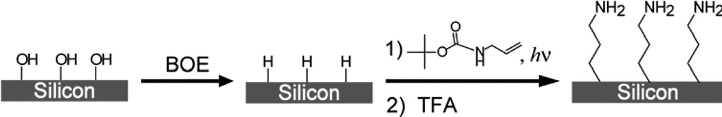
The procedure described previously37,42 was used to functionalize hydrogen terminated SiNWs with tert-Butyl allylcarbamate (Scheme 2). SiNWs were immersed in 2% HF solution for 3 seconds, washed with Millipore water and blow dried under N2 stream. The wafer was immediately placed in a custom made quartz container which was then pumped down to ~2×10⁻⁵ Torr, followed by an argon purge. Under positive argon pressure, a mixture of 1:2 tert-Butyl allylcarbamate:methanol (v/v) was applied to the wafer, completely covering the SiNWs. The wafer was illuminated with UV (254 nm, 9 mW/cm2 at 10 cm) for 3 hours. SiNWs were then rinsed in methylene chloride and methanol. The deprotection of t-Boc amine was carried out in a solution of TFA in methanol (1:4 v/v) for 4 hours, followed by extensive methanol washing.
X-ray Photoelectron Spectroscopy
X-ray photoelectron spectroscopy (XPS) was utilized to quantify the amount of oxide on Si (100) wafers after surface treatments outlined in Schemes 1 and 2. All XPS measurements were performed in an ultrahigh vacuum chamber of an M-probe surface spectrometer that has been previously described.43 Experiments were performed at room temperature, with 1486.6 eV X-ray from the Al Kα line and a 35° incident angle measured from the sample surface. ESCA-2000 software was used to collect the data. An approach described elsewhere30,43 was used to fit the Si 2p peaks and quantify the amount of surface SiOx, assuming that the oxide layer was very thin. Any peak between 100 eV and 104 eV was assigned to Si+-Si4+ and fitted as described in the literature.44 SiOx:Si 2p peak ratio was divided by a normalization constant of 0.17 for Si(100) surfaces.
Contact Angle Measurements
The sessile contact angle of water on the functionalized Si(100) surface was used to check the fidelity of surface chemistry as described in Schemes 1 and 2. Contact angle measurements were obtained with an NRL C.A. Goniometer Model #100-00 (Rame-Hart, Inc., Netcong, NJ) at room temperature. All measurements were repeated three times and averaged to obtain the contact angle θ for the surface.
Surface Plasmon Resonance (SPR)
All SPR experiments were performed on the Biacore 3000 with carboxylic acid terminated Biacore CM5 chips. The active flow cells were first primed in 1× SSC (15 mM NaCitrate, 150 mM NaCl, pH 7.5). To generate an amine surface, the carboxylic acid groups were converted to succinimide esters by flowing EDC/NHS prior to exposure of a 1 mg/ml solution of polylysine (Sigma-Aldrich, St. Louis, MO). Single stranded DNA (5’TGGACGCATTGCACAT3’, Midland Certified, Ind., Midland, TX) was electrostatically absorbed unto the polylysine matrix. Complementary DNA was then immediately introduced and allowed to hybridize to the active surface. The flow cell was regenerated with two 1 minute pulses of 50 mM NaOH, after which ssDNA was reabsorbed electrostatically before another cDNA pulse was introduced for hybridization.
Electronic Measurements
The 4-point resistivity of silicon film as well as SiNW resistances and solution gating were measured with Keithley 2400 Source Meter (Keithley Instruments, Inc., Cleveland, OH). The sensing experiments were performed with SR830 DSP Lock-in Amplifier (Stanford Research Systems, Inc., Sunnyvale, CA). A 50mVrms at 13Hz voltage source (VSD) was applied to one terminal of the nanowire, with the amplifier input operating in the current-measure mode. A platinum wire was inserted into the microchannel and used as a solution gate, while it was kept at a ground potential throughout the real-time measurements to reduce the noise in the system (Figure 1A). The devices were functionalized and assembled as described above. Single stranded 10 µM DNA (same as in SPR experiments) in 1× SSC buffer was flowed through the microchannel for 1 hr and allowed to electrostatically adsorb to the amine terminated surface of SiNWs. The non-bound DNA was washed thoroughly with 1× SSC buffer. Complementary DNA (5’ATGTGCAATGCGTCCA3’, Midland Certified, Ind., Midland, TX) of varying concentrations in 1× SSC buffer was sequentially injected from the injection PDMS chip (Supplementary Material) into the microchannel containing Si NWs at a flow rate of 2.0 µl/min as the resistance of the NWs was recorded in real time. Non-complementary DNA (noncomp. DNA) (5’CATGCATGATGTCACG3’) was used as a control. In general, a different SiNW sensor was utilized for each individual measurement described here.
Determination of Kinetic Parameters and Concentrations
To extract kon and koff values from the resistance versus time data, we used equation 6 to create a series of two equation pairs with two unknowns (one equation from each concentration) which we solved to get the implied kon and koff. For each concentration in the pair we chose to use all data points starting at a time where our model (the first term in brackets in equation 5) indicated a value of 0.63 (i.e., a time equal to the characteristic time of this exponential function) and ending 150 seconds later (time close to saturation, i.e., a value of 1 for eq. 5). We chose this part of the data because the assumptions underlying the model indicate that values close to saturation are the ones where our model fits real data the best. For each concentration pair we, therefore, had 150 pairs of equations, each yielding a value for kon and koff.
To extract the implied concentration values from the resistance versus time data, we used equation 6, this time with kon and koff values obtained from a concentration pair that did not contain the concentration we were trying to estimate. Again, we chose 150 data points from the same portion of the graph used to extract kon and koff values. Each data point yielded one equation in one unknown, which we solved to get the implied concentrations. We then calculated the average implied concentration and the standard deviation for all 150 data points (results summarized in Table 2).
Table 2.
Kinetic Parameters estimated from SiNW biosensors for the hybridization of 16-mer DNA and corresponding comparisons with analogous SPR and SPDS (surface plasmon diffraction sensor).52 The calculated concentrations (bottom row) were estimated with eq. 6, by using the pair of SiNW measurements that did not include the concentration to be determined. For example, the 1 nM and 100 nM measurements were used to determine the concentration at 10 nM. Standard deviations are given in parentheses.
| SiNWs: concentration pair: | SPR (this work) (poly-L-lysine surface, 16-mer DNA) |
SPDS (ref. 52) (avidin-biotin linkage, 15-mer DNA) |
|||
|---|---|---|---|---|---|
| 10 nM 100 nM |
1 nM 100 nM |
1 nM 10 nM |
|||
| kon (M−1 s−1) | 3.5(3.4) × 105 | 4.2(2.4) × 105 | 6.2(9.6) × 105 | 1.01 × 10⁵ | 6.58 × 10⁴ |
| koff (s−1) | 3.1 (0.5) × 10s−2 | 2.4 (0.8) × 10−2 | 2.4 (0.9) × 10−2 | 2.01 × 10⁻² | 1.32 × 10⁻⁴ |
| KA (M−1) | 1.1 × 10⁷ | 1.8 × 10⁷ | 2.6 × 10⁷ | 5.02 × 10⁶ | 4.98 × 10⁸ |
| [DNA] | 100 nM (actual); 68(52) nM calculated | ||||
| 10 nM (actual); 14(9) nM calculated | |||||
Results and Discussion
Surface Characterization
We used contact angle measurements to follow the functionalization processes of various surfaces (Table 1). The procedure in Scheme 1 generates a large increase in contact angle. Similarly, large changes in contact angles are observed for photochemically treated Si surface before and after t-Boc deprotection. The resulting contact angle of ~60° is observed for surfaces prepared by Scheme 1 and 2, arguing for an existence of chemically similar, amine terminated monolayers on these surfaces.
Table 1.
Measured contact angles for various Si(100) surfaces.
Quantifying the amount of oxide on the SOI NWs is extremely challenging. Therefore, we used Si(100) bulk surfaces to approximate the amount of surface oxide remaining after photochemical functionalization. Figure 2A shows XPS scan in the Si/SiOx region. The Si(100) surface with native oxide exhibited approximately 1.9 equivalent monolayers of SiOx. In contrast, the Si(100) surface treated according to Scheme 2 contained 0.08 equivalent monolayers of SiOx prior to TFA deprotection and 0.3 monolayers of SiOx after the deprotection step and a 10 hour exposure to 1× SSC buffer. The roughness of a SiNW surface may cause a more extensive oxidation than the one observed on the bulk surface, but the data in Fig. 1A does demonstrate a significant reduction in oxide thickness after photochemical treatment. Furthermore, we used XPS to determine the presence of amine terminated monolayer on bulk Si(100) surfaces post functionalization with two different schemes. Figure 2A inset demonstrates the XPS scans of N 1s region. Nitrogen peak is clearly visible for surfaces functionalized by Schemes 1 and 2, while no peak is present for the nonfunctionalized Si.
Figure 2.

A. XPS of Si 2p region of Si(100) surface functionalized as in Scheme 2 before (dark grey) and after (light grey) TFA deprotection and 10 hrs in 1× SSC buffer. Nonfunctionalized Si(100) surface with native oxide (black). Inset: N 1s region of nonfunctionalized Si(100) surface (black), Si(100) functionalized by Scheme 1 (light grey) and Scheme 2 (dark grey). B. Current-Voltage (IV) graphs of SiNWs functionalized by Scheme 1 in solutions of varying pH. Inset: Solution gated (VSG) n-type hydroxyl terminated SiNW in solutions of varying pH.
Scheme 1 functionalized SiNWs demonstrate a sensitivity to pH which is different than for native oxide-passivated NWs.45 The isoelectric point of silica is ~2,46 implying that for hydroxyl terminated, non-functionalized SiNWs at low pH, the SiOH groups are largely protonated. At high pH, negative charges on SiO− should deplete carriers in the n-type SiNWs, causing a decrease in IDS (Figure 2B, inset). Above pH 4 the conductance is no longer modulated by increasing the pH, as most of the hydroxyl groups are deprotonated. When the surface is functionalized with amine (pKa ~9–10), the opposite trend is expected. At low pH, the amine is protonated, causing carrier depletion or increased resistance in p-type SiNW. This trend is observed in Figure 2B, where the sharpest transition in resistance occurs between pH 9 and 10. The observation of the correct pH effects on the resistance of the SiNWs further confirms of the presence of amine surface functional groups.
As shown in Figure 3, oxide covered SiNWs in 1× SSC buffer (0.165M, pH 7.2) respond weakly to the applied solution gate voltage, VSG, showing no significant on-off current transition between 0.8 and −0.8 Volts. In contrast, directly passivated SiNWs (Scheme 2) exhibit on-off current ratios of ~102. Figure 3 strongly suggests that directly passivated SiNWs exhibit an enhanced response to surface charges and should therefore serve as superior NW sensors compared with similarly functionalized, but oxide-passivated SiNWs.
Figure 3.

Solution gating of SiNWs functionalized by Scheme 1 (grey) and by Scheme 2 (black) (VSD was 50 mV). (Right inset) IV curves of SiNWs in air with (black) and without (grey) oxide. (Left inset) Resistances in air of SiNWs functionalized by Scheme 1 (left) and Scheme 2 (right).
The Scheme 2 procedure does involve an HF etch step, which can be potentially detrimental to the device conductance. We thus checked the conductivity of SiNWs before and after photochemical treatment. Lightly doped SiNWs provide for superior FET properties,47 and, in fact, we have reported that lightly doped (1017 cm−3) p- or n-type SiNWs are more sensitive biomolecular sensors than those reported here.48 Our doping process preferentially dopes the top few nanometers of the SiNWs.49 Thus, if the HF etching of the Si surface was extensive enough, we could expect an enhancement in SiNW current modulation by VSG to be entirely due to the decrease in carrier concentration and not the removal of surface oxide. The Fig. 3 insets demonstrate that the NW resistance increased only, on average, by a factor of 2 following the HF treatment. This relatively negligible resistance increase indicates that the major reason that the SiNWs prepared by Scheme 2 exhibit an improved solution FET performance originates from the elimination of oxide via direct silicon passivation.
Nanowire Sensing Measurements
Figure 4 shows SiNW real-time detection of the electrostatic adsorption of 10 µM ssDNA, followed by the hybridization in 1× SSC buffer of 100 nM complementary DNA strand. As expected, the resistance of p-type SiNWs is decreased with the addition of negative surface charges. The metal contacts to NWs have been covered with Si3N4 layer, and there is no background conductance through the solution. We have observed an insignificant change in the resistance of the NWs upon switching from dry environment to buffer solution (data not shown). Moreover, as Figure 4 (right inset) shows, changing the ionic strength of the solution does not affect the resistance. In addition, the automated solution injection (Supporting Information) removes any baseline shifts or transient changes in the resistance when solutions are switched. SPR was also utilized in parallel to SiNWs in order to validate the surface chemistry and to obtain kinetic parameters such as kon, koff and affinity constant KA for this particular DNA pair. Poly-L-lysine was covalently attached to the SPR sensor chips, mimicking the amine terminated monolayer of SiNWs. Figure 4 (left inset) shows the SPR response to the electrostatic adsorption of a 10 µM primary DNA strand. The surface density of adsorbed DNA was estimated as 2.5×1013 cm−2, using the conversion factor of 1000RU = 100 ng cm−2 from the literature.50 The surface density is approximately an order of magnitude higher than the average surface density of 1012 cm−2 obtained when localizing biotinylated DNA on a streptavidin covered surface.52 Such high surface density of primary DNA is expected because the poly-L-lysine treated surface is positively charged. It is likely that the amine-terminated SiNW surface has less surface charges than the poly-L-lysine covered surface and thus contains fewer sites for electrostatic adsorption of oligonucleotides.
Figure 4.

Real-time response of SiNWs functionalized as in Scheme 1 to the addition of (a) 10µM ssDNA and (b) 100nM complementary DNA. Right top inset: Real-time SiNW response to the sequential addition of (a) 0.165M SSC, (b) 0.0165M SSC, and (c) 0.00165M SSC buffers. Left inset: SPR measurement demonstrating the addition of 10µM ssDNA to poly-L-lysine coated CM5 sensor chip. VSD = 50mV.
Figure 5 demonstrates real-time label free detection of ssDNA by SiNWs and by SPR. In either case, the primary DNA strand was electrostatically immobilized on the sensor surface. Known DNA concentrations were injected after a stable reading with 1× SSC buffer was obtained and the flow was maintained throughout the experiment. Different concentrations were detected with different groups of SiNWs. We observed that the hybridization on SiNWs is essentially irreversible on the relevant time scales when the analyte DNA was being washed away with the buffer solution. Such behavior is in contrast to SPR measurements, where the slow reversal of hybridization was observed (Fig. 5C). The performance of the NWs surface functionalized according to Scheme 1 (Fig. 5A) was compared to SiNW sensors prepared according to Scheme 2 (Fig. 5B). The SPR experiments, although carried out on Au substrates, also utilized primary ssDNA that was electrostatically adsorbed onto an amine terminated surface. The intention here was to find experimental conditions that could serve to validate the NW experiments by obtaining kinetic parameters for these particular DNA strands under specific experimental conditions. Control experiments with non-complementary DNA yielded no response for either SiNWs or SPR measurements (black traces of Figs 5A and 5C). These negative controls were also independently validated via fluorescent detection in microfluidic channels on two different (Scheme 1 and 2) Si surfaces (Fig. 5A and B, insets). Figure 5D demonstrates that the NW response (ΔR/Ro) varies as log[DNA]. Such a logarithmic dependence has been previously reported.48,53 As demonstrated in Figure 5D, the dynamic range of SiNWs is increased by 100 after the removal of oxide and UV-initiated chemical passivation; the limit of detection (LOD) increased from 1 nM to 10 pM.
Figure 5.

Concentration-dependent, real-time sensing of complementary DNA by SiNWs and by SPR in 0.165M electrolyte. A. Real-time responses of SiNWs that were surface functionalized according to Scheme 1 and coated with electrostatically adsorbed primary DNA. The black trace represents exposure of the SiNW sensors to 100 nM non-complementary ssDNA. Each curve represents measurements from a different set of NWs. Inset: Fluorescence image of Si(100) surface (with overlaying PDMS microfluidics chip) treated as in Scheme 1 followed by 10µM primary DNA addition and addition of (microchannel a) 100nM noncomplementary fluorescent DNA and (microchannel b) 100nM complemenatary fluorescent DNA. PDMS chip was removed before the image was collected. B. As in A, except the SiNWs were functionalized according to Scheme 2. Inset: Same as in A inset, but Si(100) surface was treated as in Scheme 2. C. SPR measurement of the hybridization of complementary DNA to electrostatically adsorbed primary DNA on a poly-L-lysine surface. D. Normalized SiNW responses for Scheme 1 (black dots) and Scheme 2 (red dots) surface preparations, as a function of the log of DNA concentration. For all measurements, VSD = 50mV.
Nanowires as Quantitative Biomolecular Sensors
SiNW sensors can potentially be utilized to quantitate analyte concentration and binding constants. In order to explore this possibility, the SiNW sensing response must be compared with other label-free, real-time methods such as SPR. It is also critical to design experimental parameters for both sensing modalities that are as similar as possible, as was described above. In this section, we first discuss the use of electrostatically adsorbed primary DNA for detecting complementary DNA analyte. We then discuss the development of a self-consistent model that allows for the direct comparison of SPR measurements with nanowire sensing data. Finally, we test that model by utilizing the nanowire sensing data to calculate 16-mer DNA binding constants and analyte concentrations.
Previous studies have demonstrated that the Langmuir model can be applied for parameterization of the hybridization processes of short oligonucleotides.19,52 We used the Langmuir model to calculate kinetic parameters from the SPR hybridization measurements (Fig. 5C) and obtained kon=1×10⁵, koff=2×10⁻², KA=5×10⁶ (Table 2). This KA value is between 10 and 100 times smaller than that reported for similar length DNA measured with a quartz crystal microbalance, SPR,19 and surface plasmon diffraction sensors (SPDS).52 The average primary DNA surface coverage in those studies was ~5×10¹² molecules/cm2.19,52 As stated above, the electrostatically adsorbed DNA coverage in our SPR experiments was approximately 10 times higher, at 2.5×1013 cm−2. This difference in coverage likely arises from the differing methods of DNA immobilization; while in our system the DNA is electrostatically adsorbed, other studies utilized a streptavidin-biotinylated DNA linkage for surface immobilization.19,52 High surface coverage of primary DNA significantly reduces the efficiency of hybridization.51,52 In addition, the hybridized duplex of electrostatically adsorbed and covalently bound DNA may be structurally and energetically different. It has been proposed that a preferred structural isomer of an oligonucleotide pair on a positively charged surface is a highly asymmetrical and unwound duplex.54 It is possible that the non-helical nature of such a DNA duplex, together with steric effects associated with a highly packed surface, play major roles in the reduced affinity for the 15-mer pair used in this study.
We now turn toward developing a model for using SiNW sensors to quantitate complementary DNA pair binding constants, and, if those numbers are known, to determine the solution concentration of the analyte. A discussion of the kinetics of a surface binding assay, as measured within flowing microfluidics environments, is required. Zimmermann and coworkers modeled the kinetics of surface immunoassays in microfluidics environments.55 Their model was based on four differential equations: the two Navier-Stokes partial differential equations, the Convection-Diffusion equation, and the ordinary differential equation resulting from the Langmuir binding model (i.e. the binding/hybridization equilibrium). A key result was that in the limit of high analyte flow speeds (> 0.5 mm/sec) (which is the case for all the experiments here) the amount of analyte that is captured and ready for detection can be described by the ordinary differential equation resulting from the Langmuir binding model:
| (1) |
Here, Θt =surface density of bound analyte molecules; kon =rate constant for association; koff =rate constant for dissociation; C=solution concentration of analyte (a constant under flowing conditions); Θmax = maximum number of binding sites available per surface area. Eq. (1) can be solved analytically:
| (2) |
The challenge is to translate from the resistance change of a SiNW sensor to the analyte concentration, C. However, the exact relationship between a measured resistance change and the surface density of bound analyte molecules is not intuitively clear. Here we attempt to determine the nature of that relationship.
We demonstrated above (Fig. 5D) that the cumulative change in SiNW sensor resistance arising from the binding of a charged analyte (ssDNA) at a concentration-dependent saturation was linearly proportional to the log[DNA], similar to what has been reported for VLS SiNW detection of prostate specific antigen (PSA).53 In mathematical terms, this means that as we approach saturation for a given concentration:
| (3) |
where α is a constant, ΔR=R−Ro, R is resistance at time t, and Ro is the resistance at t=0. At saturation levels eq. 2 reduces to (where the binding affinity ). In the limit where KAC ≪ 1 (which is usually the case with values of C ≤ 10−9 and values of KA < 108), this reduces to Θt = KAΘmaxC. Therefore, at saturation, and with KAC ≪ 1, Θt scales linearly with C. From our previous discussion, this implies that at saturation scales logarithmically with Θt (or equivalently that Θt is an exponential function of at saturation). In estimating the relationship between resistance changes at all times (not just at saturation) and the surface density of bound analyte molecules at all corresponding times, we start by assuming the same functional relationship that we experimentally observe at saturation. We also impose two boundary conditions. (1) When the measured resistance reaches its saturation level we would expect the maximum number of binding events to have taken place and for that number to be consistent with the prediction from the Langmuir binding model (eq. 2). (2) When the measured resistance is unchanged from its starting level we expect zero binding events (again consistent with the Langmuir model at time = 0). Based on these assumptions and boundary conditions we can thus estimate that the surface density of bound analyte molecules as a function of resistance change has the form:
| (4) |
The validity of eq. 4 can be tested by considering the following expression that is derived from eq. 4 and comparing it to the same expression derived from eq. 2:
| (5) |
Note that eq. 5 is expressing the fraction of bound analyte molecules at time t relative to the level at saturation in terms of ΔR (first term in brackets) and in terms of binding constants (second term in brackets). Time appears explicitly in the second term in brackets, while it is implicit in the first term in brackets (i.e., at a given time t there is a given R and ΔR). If we plot the first term in brackets in eq. 5 (the term containing ΔR) against the second term in brackets (using kon and koff values from an SPR analysis), we find that the two curves are similar (Fig. 6).
Figure 6.

Comparison of SPR-derived hybridization kinetic parameters with NW sensing data. The black line represents eq. 5 plotted using kon and koff obtained from SPR measurements, β =(konC+koff)t. The grey trace is obtained from SiNW resistance versus time data, . C=10 nM.
A second test of eq. 4 is to utilize it to extract binding kinetics. As we can infer from eq. 5, if eq. 4 is equivalent to the Langmuir binding model (eq. 2), then:
| (6) |
We can thus extract kon and koff values from measured resistance data. We can select R versus time traces at any two concentration values. Taking R and ΔR at an arbitrary point in time and noting Rmax (the resistance at saturation), we have two equations (one for each concentration C) and two unknowns. We thus solve for kon and koff and compare directly with kinetic parameters obtained from SPR experiments. The kon, koff, and KA values are summarized in Table 2. The kon constants determined from the SiNW experiments are 3–5 times larger than kon obtained with SPR experiments. The nanowire-measured koff values, however, are consistently quite close to those measured with SPR. As stated above, the variation in kon values may be a reflection of steric affects that arise from the unusually high surface density of primary DNA adsorbed onto the poly-L-lysine surfaces that were used for the SPR experiments.51,52
Further work has to be done to ground this translation from nanowire resistance readings to the Langmuir binding model (or equivalently from resistance readings to number of bound analyte molecules) on firm theoretical grounds. It is encouraging, however, that with our resistance data we can extract useful binding kinetics. The most useful application of our model would be in extracting otherwise unknown concentration values once kon and koff values are known. As demonstrated here and elsewhere, SiNW sensors can be used for label-free biomolecule detection at concentrations significantly below the limits of detection for SPR. Thus, the potential for SiNW sensors to quantitate analyte concentrations when the concentrations are below 10 nM represents a nontrivial application. The consistency of the SiNW measurements that is reflected in the Table 2 values is worth noting, especially since each measurement was carried out using a different SiNW sensor. This provides validation that the nanofabrication techniques that were utilized to prepare the NW sensing devices are highly reproducible.
Conclusion
Real-time label free detection of DNA 16mers with SiNWs in physiologically relevant 0.165M electrolyte solution was performed. Primary DNA was electrostatically adsorbed onto an amine terminated SiNW surface and hybridized to the complementary strand in a microfluidics channel under flow. Electrostatic adsorption of ssDNA to poly-L-lysine coated surface has previously been electronically detected at nanomolar concentrations with capacitive methods on highly doped Si electrodes in 0.015M solution.56 The ability to detect DNA under physiological conditions, as demonstrated in this work, is of significance as it may allow the direct use of biological samples such as serum or tissue culture media. It is likely that because the primary DNA is electrostatically bound and hybridization occurs very close to NW surface, Debye screening does not prevent SiNW based detection. Moreover, DNA hybridization is more efficient under high ionic strength conditions.10,19,51 We attempted to carry out hybridization in pure water; however, no changes in SiNW resistance were observed (data not shown), presumably because DNA-DNA repulsion is significant in that case.
SiNWs with significantly reduced oxide coverage exhibited enhanced solution FET characteristics (Fig. 3) when compared to SiNWs characterized by a native SiO2 surface passivation. Oxide covered, highly doped SiNWs were designed to exhibit a similar dynamic range of DNA detection as the best near-infrared imaging SPR technique.57 − 10nM for 18mer, corresponding to ~1011 molecules/cm2. When identical nanowires were functionalized by the UV-initiated radical chemistry method, resulting in near-elimination of the Si-SiO2 interface, the limit of detection was increased by two orders of magnitude, with an accompanying increase in the dynamic range. This result highlights the importance of controlling surface chemistry of SiNWs for their optimization as biological sensors. In the future, surface chemistries yielding higher coverage than UV-initiated alkylation may be utilized to passivate and electrochemically convert SiNWs into arrays for multiparameter analysis.58,59
Finally, a model that is consistent with both the standard Langmuir binding model and with the experimentally measured electrical response of SiNW sensors to the detection of complementary DNA was developed. The model yields results for an oligonucleotide pair binding affinities that are at least consistent with those measured by more standard methods such as SPR. The potential for SiNW sensors to quantitate the concentrations of low-abundance biomolecules within physiological relevant environments is an intriguing one, and we are currently vigorously pursuing this possibility.
Supplementary Material
Acknowledgment
The XPS measurements were carried out at the Molecular Materials Research Center of the Beckman Institute at Caltech. We thank Professor Björkman for assistance with the SPR measurements. This work was funded by the National Cancer Institute #5U54 CA119347 (JRH, PI) and through a subcontract from the MITRE Corporation. YSS acknowledges the Samsung Foundation for a graduate fellowship.
Footnotes
Supporting Information Available: Details of the fabrication and assembly of the microfluidics sample injection chip and complete references 6 and 38.
References
- 1.Kong J, Franklin NR, Zhou CW, Chapline MG, Peng S, Cho KJ, Dai H. Science. 2000;287:622. doi: 10.1126/science.287.5453.622. [DOI] [PubMed] [Google Scholar]
- 2.Patolsky F, Lieber CM. Mater. Today. 2005;8:20. [Google Scholar]
- 3.Park SJ, Taton TA, Mirkin CA. Science. 2002;295:1503. doi: 10.1126/science.1067003. [DOI] [PubMed] [Google Scholar]
- 4.Ziegler C. Analytical and Bioanalytical Chemistry. 2004;379:946. doi: 10.1007/s00216-004-2694-y. [DOI] [PubMed] [Google Scholar]
- 5.Lasseter TL, Cai W, Hamers RJ. Analyst. 2004;129:3. doi: 10.1039/b307591e. [DOI] [PubMed] [Google Scholar]
- 6.Davidson EH, et al. Science. 2002;295:1669. doi: 10.1126/science.1069883. [DOI] [PubMed] [Google Scholar]
- 7.Kitano H. Science. 2002;295:1662. doi: 10.1126/science.1069492. [DOI] [PubMed] [Google Scholar]
- 8.Hood L, Heath JR, Phelps ME, Lin B. Science. 2004;306:640. doi: 10.1126/science.1104635. [DOI] [PubMed] [Google Scholar]
- 9.Chen RJ, Bangsaruntip S, Drouvalakis KA, Kam NWS, Shim M, Li Y, Kim W, Utz PJ, Dai H. Proc. Natl. Acad. Sci. U.S.A. 2003;100:4984. doi: 10.1073/pnas.0837064100. [DOI] [PMC free article] [PubMed] [Google Scholar]
- 10.Star A, Tu E, Niemann J, Gabriel J-CP, Joiner S, Valcke C. Proc. Nat. Acad. Sci. USA. 2006;103:921. doi: 10.1073/pnas.0504146103. [DOI] [PMC free article] [PubMed] [Google Scholar]
- 11.Besteman K, Lee J, Wiertz FGM, Heering HA, Dekker C. Nano Lett. 2003;3:727. [Google Scholar]
- 12.Hahm J, Lieber CM. Nano Lett. 2004;4:51. [Google Scholar]
- 13.Li Z, Chen Y, Li X, Kamins TI, Nauka K, Williams RS. Nano Lett. 2004;4:245. [Google Scholar]
- 14.Li C, Curreli M, Lin H, Lei B, Ishikawa FN, Datar R, Cote RJ, Thompson ME, Zhou C. J. Am. Chem. Soc. 2005;127:12484. doi: 10.1021/ja053761g. [DOI] [PubMed] [Google Scholar]
- 15.Ramanathan K, Bangar MA, Yun M, Chen W, Myung NV, Mulchandani A. J. Am. Chem. Soc. 2005;127:496. doi: 10.1021/ja044486l. [DOI] [PubMed] [Google Scholar]
- 16.Lud SQ, Nikolaides MG, Haase I, Fischer M, Bausch AR. ChemPhysChem. 2006;7:379. doi: 10.1002/cphc.200500484. [DOI] [PubMed] [Google Scholar]
- 17.Israelachvili J. Intermolecular and Surface Forces. London: Academic Press; 1985. [Google Scholar]
- 18.Zheng GF, Patolsky F, Cui Y, Wang WU, Lieber CM. Nat. Biotech. 2005;23:1294. doi: 10.1038/nbt1138. [DOI] [PubMed] [Google Scholar]
- 19.Okahata Y, Kawase M, Niikura K, Ohtake F, Furusawa H, Ebara Y. Anal. Chem. 1998;70:1288. doi: 10.1021/ac970584w. [DOI] [PubMed] [Google Scholar]
- 20.Li Z, Rajendran B, Kamins TI, Li X, Chen Y, Williams RS. Appl. Phys. A. 2005;80:1257. [Google Scholar]
- 21.Vieu C, Carcenac F, Pepin A, Chen Y, Mejias M, Lebib A, Manin-Ferlazzo L, Couraud L, Launois H. Ap. Surf. Sci. 2000;164:111. [Google Scholar]
- 22.Yang PD. MRS Bulletin. 2005;30:85. [Google Scholar]
- 23.Heath JR, LeGoues FK. Chem. Phys. Lett. 1993;208:263. [Google Scholar]
- 24.Morales A, Lieber CM. Science. 1998;279:208. doi: 10.1126/science.279.5348.208. [DOI] [PubMed] [Google Scholar]
- 25.Chung SW, Yu JY, Heath JR. Appl. Phys. Lett. 2000;76:2068. [Google Scholar]
- 26.Melosh NA, Boukai A, Diana F, Gerardot B, Badolato A, Petroff PM, Heath JR. Science. 2003;300:112. doi: 10.1126/science.1081940. [DOI] [PubMed] [Google Scholar]
- 27.Beckman RA, Johnston-Halperin E, Melosh NA, Luo Y, Green JE, Heath JR. J. Appl. Phys. 2004;96:5921. [Google Scholar]
- 28.Yablanovitch E, Allara DL, Chang CC, Gmitter T, Bright TB. Phys. Rev. Lett. 1986;57:249. doi: 10.1103/PhysRevLett.57.249. [DOI] [PubMed] [Google Scholar]
- 29.Sham TK, Naftel SJ, Kim P-SG, Sammynaiken R, Tang YH, Coulthard I, Moewes A, Freeland JW, Hu Y-F, Lees ST. Phys. Rev. B. 2004;70 045313/1. [Google Scholar]
- 30.Webb LJ, Lewis NS. J. Phys. Chem. B. 2003;107:5404. [Google Scholar]
- 31.Bansal A, Lewis NS. J. Phys. Chem. B. 1998;102:4058. [Google Scholar]
- 32.Haick H, Hurley PT, Hochbaum AI, Yang P, Lewis NS. J. Am. Chem. Soc. 2006;128:8990. doi: 10.1021/ja056785w. [DOI] [PubMed] [Google Scholar]
- 33.Terry J, Mo R, Wigren C, Cao RY, Mount G, Pianetta P, Linford MR, Chidsey CED. Instrum. Methods. Phys. Res. Sect. B. 1997;133:94. [Google Scholar]
- 34.Effenberger F, Gotz G, Bidlingmaier B, Wezstein M. Angew. Chem. Int. Ed. Engl. 1998;37:2462. doi: 10.1002/(SICI)1521-3773(19981002)37:18<2462::AID-ANIE2462>3.0.CO;2-R. [DOI] [PubMed] [Google Scholar]
- 35.Boukherroub R, Wayner DDM. J. Am. Chem. Soc. 1999;121:11513. [Google Scholar]
- 36.Cicero RL, Linford MR, Chidsey CED. Langmuir. 2000;16:5688. [Google Scholar]
- 37.Streifer JA, Kim H, Nichols BM, Hamers RJ. Nanotechnology. 2005;16:1868. [Google Scholar]
- 38.Jönsson U, et al. BioTechniques. 1991;11:620. [PubMed] [Google Scholar]
- 39.Wang D, Sheriff BA, Heath JR. Nano Lett. 2006;6:1096. doi: 10.1021/nl052558g. [DOI] [PubMed] [Google Scholar]
- 40.Duffy DC, McDonald JC, Schueller OJA, Whitesides GM. Anal. Chem. 1998;70:4974. doi: 10.1021/ac980656z. [DOI] [PubMed] [Google Scholar]
- 41.Unger MA, Chou HP, Thorsen T, Scherer A, Quake SR. Science. 2000;288:113. doi: 10.1126/science.288.5463.113. [DOI] [PubMed] [Google Scholar]
- 42.Bunimovich YL, Ge G, Beverly KC, Ries RS, Hood L, Heath JR. Langmuir. 2004;20:10630. doi: 10.1021/la047913h. [DOI] [PubMed] [Google Scholar]
- 43.Haber JA, Lewis NS. J. Phys. Chem. B. 2002;106:3639. [Google Scholar]
- 44.Himpsel FJ, McFeeley FR, Taleb-Ibrahimi A, Yarmoff JA, Hollinger G. Phys. Rev. B. 1988;38:6084. doi: 10.1103/physrevb.38.6084. [DOI] [PubMed] [Google Scholar]
- 45.Cui Y, Wei Q, Park H, Lieber CM. Science. 2001;293:1289. doi: 10.1126/science.1062711. [DOI] [PubMed] [Google Scholar]
- 46.Hu K, Fan F, Bard AJ, Hillier AC. J. Phys. Chem. B. 1997;101:8298. [Google Scholar]
- 47.Cui Y, Duan X, Hu J, Lieber CM. J. Phys. Chem. B. 2000;104:5213. [Google Scholar]
- 48.Cheng MM-C, Cuda G, Bunimovich YL, Gaspari M, Heath JR, Hill HD, Mirkin CA, Nijdam AJ, Terracciano R, Thundat T, Ferrari M. Curr. Opin. Chem. Biol. 2006;10:11. doi: 10.1016/j.cbpa.2006.01.006. [DOI] [PubMed] [Google Scholar]
- 49.Beckman R, Johnston-Halperin E, Luo Y, Green JE, Heath JR. Science. 2005;310:465. doi: 10.1126/science.1114757. [DOI] [PubMed] [Google Scholar]
- 50.Stenberg E, Persson B, Roos H, Urbaniczky C. J. Colloid Interface Sci. 1991;143:513. [Google Scholar]
- 51.Peterson AW, Heaton RJ, Georgiadis RM. Nucleic Acids Res. 2001;29:5163. doi: 10.1093/nar/29.24.5163. [DOI] [PMC free article] [PubMed] [Google Scholar]
- 52.Yu F, Yao D, Knoll W. Nucleic Acids Res. 2004;32:e75. doi: 10.1093/nar/gnh067. [DOI] [PMC free article] [PubMed] [Google Scholar]
- 53.Zheng G, Patolsky F, Cui Y, Wang WU, Lieber CM. Nat. Biotech. 2005;23:1294. doi: 10.1038/nbt1138. [DOI] [PubMed] [Google Scholar]
- 54.Lemeshko SV, Powdrill T, Belosludtsev YY, Hogan M. Nucleic Acids Res. 2001;29:3051. doi: 10.1093/nar/29.14.3051. [DOI] [PMC free article] [PubMed] [Google Scholar]
- 55.Zimmermann M, Delamarche E, Wolf M, Hunziker P. Biomed. Microdevices. 2005;7:99. doi: 10.1007/s10544-005-1587-y. [DOI] [PubMed] [Google Scholar]
- 56.Fritz J, Cooper EB, Gaudet S, Sorger PK, Manalis SR. Proc. Nat. Acad. Sci. USA. 2002;99:14142. doi: 10.1073/pnas.232276699. [DOI] [PMC free article] [PubMed] [Google Scholar]
- 57.Nelson BP, Grimsrud TE, Liles MR, Goodman RM, Corn RM. Anal. Chem. 2001;73:1. doi: 10.1021/ac0010431. [DOI] [PubMed] [Google Scholar]
- 58.Nemanick EJ. Caltech Ph.D. Thesis. 2005. Chemical and Electrical Passivation of Single Crystal Silicon Surfaces through Covalently Bound Organic Monolayers. [Google Scholar]
- 59.Rohde RD, Agnew HD, Yeo W-S, Bailey RC, Heath JR. J. Am. Chem. Soc. 2006;128:9518. doi: 10.1021/ja062012b. [DOI] [PMC free article] [PubMed] [Google Scholar]
Associated Data
This section collects any data citations, data availability statements, or supplementary materials included in this article.