

Abstract
Positron emission tomography (PET) is used in the clinic and in vivo small animal research to study molecular processes associated with diseases such as cancer, heart disease, and neurological disorders, and to guide the discovery and development of new treatments. This paper reviews current challenges of advancing PET technology and some of newly developed PET detectors and systems. The paper focuses on four aspects of PET instrumentation: high photon detection sensitivity; improved spatial resolution; depth-of-interaction (DOI) resolution and time-of-flight (TOF). Improved system geometry, novel non-scintillator based detectors, and tapered scintillation crystal arrays are able to enhance the photon detection sensitivity of a PET system. Several challenges for achieving high resolution with standard scintillator-based PET detectors are discussed. Novel detectors with 3-D positioning capability have great potential to be deployed in PET for achieving spatial resolution better than 1 mm, such as cadmium-zinc-telluride (CZT) and position-sensitive avalanche photodiodes (PSAPDs). DOI capability enables a PET system to mitigate parallax error and achieve uniform spatial resolution across the field-of-view (FOV). Six common DOI designs, as well as advantages and limitations of each design, are discussed. The availability of fast scintillation crystals such as LaBr3, and the silicon photomultiplier (SiPM) greatly advances TOF-PET development. Recent instrumentation and initial results of clinical trials are briefly presented. If successful, these technology advances, together with new probe molecules, will substantially enhance the molecular sensitivity of PET and thus increase its role in preclinical and clinical research as well as evaluating and managing disease in the clinic.
Keywords: Positron Emission Tomography (PET), Photon Sensitivity, Spatial Resolution, Scintillation Detector, Semiconductor Detector, Depth-of-Interaction (DOI), Time-of-Flight (TOF)
1. INTRODUCTION
Positron emission tomography (PET) is a non-invasive medical imaging tool widely used in both clinical and pre-clinical research to study the molecular bases and treatments of disease. In clinical applications, PET has proven its critical value in several areas such as cancer diagnosing and staging, assessing neurological diseases such as Alzheimer’s disease and dementias, myocardium blood flow and viability evaluation in cardiology, as well as an increasing role in radiotherapy treatment planning and chemotherapy monitoring [1–4]. In recent years, PET is also being actively used in small animal research using new molecular probes labeled with positron emitting radionuclides, with the intention to target, detect, visualize, and quantify various extra- and intracellular molecules and processes associated with cancer, heart disease, and neurological disorders. Exotic applications using small animal PET include studying protein-protein interaction in signal transduction pathways [5,6], cell trafficking as cancer cells metastasize to different organs [7,8], therapeutic stem cells and their progeny [9,10], interaction of the immune system and tumor cells over time [11,12], gene delivery and expression in living animals to optimize the delivery of a specific gene to a chosen target [13,14], and low levels of endogenous messenger ribonucleic acid (mRNA) [15].
First, we provide a brief description of a PET system and some terms to be used in this review. A tracer compound labeled with a positron emitting radionuclide is injected to the object to visualize biochemical events. The radionuclide decays and the resulting positrons subsequently annihilate with electrons after travelling a short distance within the subject. Each annihilation produces two 511 keV photons emitted most of the time in opposite directions and these photons are detected by the detectors, which usually consist of scintillation materials, photodetectors and front-end electronics. The signal of each photon from every pair coincidence event is processed individually for spatial, energy, and arrival time information. For a pair coincidence event, if the energy of two photons stays within a preset energy window (~20–30% full-width-half-maximum (FWHM) centered on the 511 keV photopeak) and the timing difference stays within a preset time window (6–12 ns), a coincidence event will be registered and constitutes a line-of-response (LOR) for image reconstruction. In PET, there are three types of coincidence events. True coincidences (T) are the good coincident photon events where the LOR between the two coincident photons recorded on either side of the system essentially passes through their point of emission. Random coincidences (R) are a source of undesirable background counts that occur when two distinct nuclei each decay nearly at the same time and only one photon from each decay is detected within the system coincidence time window setting. Randoms rates are reduced with lower detected single photon count rates (singles) and a narrower coincidence time window setting. It is desirable to have excellent coincidence time resolution so that a narrow coincidence time window setting during data acquisition may be employed to reject randoms without compromising photon sensitivity. Scatter coincidences (S) are another undesirable source of background events that occur when one or both annihilation photons emitted from the same nucleus or single photons emitted from two separate nuclei undergo one or more Compton scatter interactions in the tissue before detection. Since scatter causes a photon to lose energy, its effects may be substantially reduced through the use of a very narrow energy window setting around the 511 keV photopeak. Again, it is also desirable to have excellent energy resolution so that a narrow energy window setting may be employed to reject scattered singles and coincidences without compromising photon sensitivity. A widely used metric, reflecting the signal-to-noise ratio (SNR) performance of PET data in the context of the three types of coincidences, is noise equivalent counts (NEC) [16] shown in formula (1).
| (1) |
Where T, S, and R are the total number of true, scatter and random coincidences, respectively. k is a number between 1 and 2, depending on phantoms/organs being imaged and the random estimation methods being used. A higher NEC at a given injection dose implies that a PET system is able to achieve better SNR and contrast-to-noise ratio (CNR) performance.
In this review, we will focus on four advances in recent small animal and whole body PET system instrumentations: 1) high photon detection sensitivity; 2) improved spatial resolution; 3) depth-of-interaction (DOI) design; 4) time-of-flight (TOF) PET.
2. PHOTON DETECTION SENSITIVITY
High photon sensitivity is a critical issue in PET instrumentation as it enables high statistical quality of acquired data, which is required to realize the system resolution potential in the reconstructed images [17,18]. High photon sensitivity would also lead to a higher NEC in formula (1). For a PET system, the photon sensitivity is determined by two factors [19]: geometric efficiency (Eg) which consists of solid angle coverage of the detectors, and intrinsic coincidence detection efficiency (Ei) which is determined by the detector atomic number (Z), density, and thickness in the path of the 511 keV photons, crystal packing fraction, as well as the coincidence time and energy window settings. The overall system photon sensitivity (Es) is given by formula (2). The photon sensitivity is often quoted for a point positron source placed at the system center. For a standard clinical whole body PET system (~700–800 mm diameter bore), Es is normally around ~0.5–1% [19,20]; for a typical small animal PET system scanner (~100–200 mm diameter bore), Es is normally around 1.0–9.0% [21,22].
| (2) |
Eg is dependent on the total solid angle of a PET system. In general, the total solid angle can be increased by either moving detectors closer to the subject, or by increasing the system coverage with more detectors. Several solutions to address this issue include: 1) extending the axial field of view of a cylindrical system as deployed recently in Siemens Biography64 TruePoint PET/CT whole body scanner [23]; 2) decreasing the system diameter [19]; 3) modifying the system geometry from cylindrical shape to other geometries [19].
There are several ways to increase Ei. The most straightforward way is to utilize scintillation materials with high Z and density (see Table 1), increasing the length of crystals, and/or packing them more tightly. However, longer crystals are associated with spatial resolution degradation towards the edge of FOV (also known as the parallax error [24]) and reduced light signal [18], to be discussed later. In addition, Ei may be increased by using monolithic scintillation crystals [25–27], by stacking semiconductor detectors slabs such as cadmium-zinc-telluride (CZT) [19, 28–31], and by using tapered crystal arrays [32]. Essentially, these efforts intend to decrease the gaps both in-between crystal pitches and between detector modules. In small diameter animal scanners based on ring geometry, these gaps can be a significant factor in limiting the photon sensitivity.
Table 1.
Common Scintillators for PET Imaging
| Scintillator | Density (g/cm3) | Effective Atomic Number (Z) | Linear Attenuation Coefficient (cm−1) | Decay Time (ns) | Light output (light photons/MeV Annihilation Photon) |
|---|---|---|---|---|---|
| NaI | 3.67 | 50.8 | 0.35 | 230 | 41,000 |
| Bi4(GeO4)3 (BGO) | 1.06 | 75.2 | 0.96 | 300 | 7,000 |
| Lu2(SiO4)O:Ce (LSO) | 7.40 | 66.4 | 0.86 | 40 | 26,000 |
| Gd2(SiO4)O:Ce (GSO) | 6.71 | 59.4 | 0.70 | 60 | 10,000 |
| Cd0.9Zn0.1Te (CZT) | 5.61 | 48 | 0.50 | N/A | 200,000 |
| BaF2 | 4.89 | 56 | 0.45 | 2 | 2,000 |
| LaBr3 | 5.06 | 48 | 0.47 | 21 | 60,000 |
As an example, consider a dual-panel breast dedicated PET system based on CZT detector technology as shown in Fig. (1). A simulation study indicates that for 4 cm panel separation and a point source, the system photon sensitivity can reach 32.5% at the center of FOV and can achieve >15% on average across the whole FOV [33]. This is over an order of magnitude higher than the standard whole body clinical system (~1–2% at the isocenter) [19,20]. The increased photon sensitivity of the CZT system is attributed to the dual-panel configuration, close proximity to the breast, high packing fraction of the CZT detectors (>99%), and the minimum of 4 cm detector thickness seen by incoming photons shown in Fig. (1a). For an 8×8×8 cm3 box-shape CZT PET system for small animal imaging shown in Fig. (1b), an increase to ~30% in the photon detection sensitivity can be obtained, which is much higher compared to standard small animal PET systems [19].
Fig. (1).

(a) Illustration of a dual panel CZT-based PET system for breast cancer imaging. Each panel has dimensions of 4×12×15 cm3. Each detector module has dimensions of 4×4×0.5 cm3 with 25-μm inter-module spacing, giving a packing fraction of over 99%.) The cross-strip readout scheme for CZT detectors with sets of parallel anode and cathode strips is deployed in order to limit the number of electronic readout channels. The anode and cathode electrodes can have different widths depending on resolution requirements. (b) Illustration of a box-shape CZT-based small animal PET system of 8×8×8 cm3 field-of-view. (Adapted from [30, 31, 33].
Another group studied tapered PET detectors and compared their performance against rectangular PET detectors [32]. This study is based on a small animal PET scanner with an inner diameter of 6 cm and an outer diameter of 10 cm. The tapered crystals significantly reduce dead area in-between detector modules and thus increase the system packing fraction as shown in Fig. (2). The traditional rectangular detector is a 14 × 14 array of 0.5 × 0.5 × 20 mm3 LSO crystals, while the tapered detector is a 14 × 14 array of 0.5 × 0.875 mm2 crystals (average height: 20 mm). The crystal element width is uniform in the axial direction but tapered in the transaxial dimension. Using the tapered arrays, the system exhibits ~4.2% photon sensitivity at the center of FOV while the system with non-tapered crystals exhibits ~3.0% at the center of FOV. No significant difference was found for the spatial resolution between the two configurations.
Fig. (2).

(a) The concept of using tapered crystals for small animal PET systems to reduce the dead area in between detector modules (assuming a bore of 10 cm diameter, each detector module has a cross-section area of 1×1 cm2 and crystals of 2 cm length). (b) Photograph of a tapered LSO array next to a rectangular LSO array and illustration of the dimensions of the simulated tapered LSO array. Note that there is no tapering along the axial direction. Adapted from [32].
It should be noted again that Ei is also dependent on the coincidence time (~2× time resolution) and energy window (~2× energy resolution at 511 keV photopeak) settings in a PET system as only those events staying within the windows are recorded. In general, if other conditions remain the same, a system that exhibits better energy resolution and time resolution would have a larger Ei.
3. SPATIAL RESOLUTION
An important question is whether PET systems have achieved the fundamental spatial resolution limit inherent to PET. This question is especially relevant to high resolution (i.e. < 2 mm) small animal PET instrumentation. A general framework with regard to spatial resolution has been proposed by Moses et al based on the measurements with multiple whole body clinical PET scanners [34].
| (3) |
The contributions to spatial resolution near the center of a tomography are the crystal size, crystal decoding process (factor b), annihilation photon acollinearity, positron range, and reconstruction algorithm. All factors in the unit of mm, d: crystal pitch, D: scanner diameter, R: effective positron range, b: a factor empirically determined from BGO (see Table 1) block detectors that ranges from 0 to 2.2 depending on detector design.
Using a similar framework, there have been several studies trying to investigate the spatial resolution limit of PET systems. Levin et al found that for a point source of 18F in water-equivalent tissue determined by three blurring factors (positron range, photon a collinearity, and crystal pitch), 750 μm FWHM resolution is attainable with 1 mm crystal pitch and 20 cm system diameter [35], provided there are adequate counts to reconstruct at that desired resolution with acceptable SNR. In addition, Stickel et al proposed a model for studying the intrinsic spatial resolution by considering the intrinsic positioning uncertainty of high-energy photons inside various detector materials, as well other blurring factors. The results indicate that 500 μm FWHM resolution is possible if 250 μm crystal pitch and 8 cm system diameter can be manufactured [36]. Motivated by the simulation work, the group is working towards scintillation block detectors of 500 μm and 750 μm LSO crystal pitch [37], which will be discussed in more details below.
It seems clear from these results that to increase PET spatial resolution, one should be able to build a PET system with as small crystal pixels and system diameter (or distance between opposing detectors) as possible. However, with standard detector design, the system diameter cannot be reduced due to the parallax error (section 4). Below, we briefly discuss several challenges faced by reducing the crystal pitch to less than 1 mm, as well as several promising solutions under investigation.
3.1. Complex and Expensive Assembly
A major challenge of manufacturing PET detectors with smaller (e.g., <2 mm width) scintillation crystal elements is that cutting, surface treatments, and assembling crystals to make arrays are complex and expensive processes. Furthermore, in order to avoid the optical cross talk between adjacent crystals, optical reflectors are usually required to be inserted, with a minimum thickness about 50–75 μm. Assuming a single crystal pitch of 250 μm is used, the optical reflectors in-between crystal pitches would degrade the packing fraction to ~60–70%, ultimately reducing the photon sensitivity.
3.2. Reduced Scintillation Light Output
In order to achieve high photon detection sensitivity, the crystals need to be thick and the thickness depends on the atomic number and density of detector materials (e.g., 20 mm for LSO material). On the other hand, the crystal pitch should be as small as possible in order to localize incoming photons with high precision. As a result, a typical PET detector comprises a long yet very narrow scintillation crystal elements of low aspect ratio (i.e. the ratio of crystal width to crystal height), which compromises the scintillation light output [18, 38, 39]. As shown in Fig. (3) the longer and narrower the crystal element, the less light collected from one end. Ultimately a weak scintillation light signal negatively impacts energy and temporal resolution performance (which affect energy and time window settings), and also limits the degree of spatial decoding. Modest light collection improvements can be made by proper treatment of the crystal faces [38,39], such as polishing or well-controlled etching, to enhance total internal reflection. Higher crystal refractive index also generally improves the probability of total internal reflection to facilitate light collection [39]. Ground surfaces do not promote total internal reflection, and so there is no significant variation of the light collection efficiency existing among different materials for that treatment as shown in Fig. (3). To address the issue of light loss, in 2 mm resolution PET systems built to date, relatively short (~10 mm length) crystals are used [40–44]. This severely compromises intrinsic 511 keV photon detection efficiency, which is ~82% for a 20 mm long crystal and ~58% for a 10 mm long crystal (assuming the linear attenuation coefficient of LSO is 0.86/cm). Similarly, in a PET system utilizing even smaller crystal pitch (i.e., 500 μm), the crystal length also needs to be reduced to compensate for light trapping within crystals.
Fig. (3).

Monte Carlo simulation of light collection efficiency from the ends of (a) 2×2×10 mm3 and (b) 1×1×10 mm3 crystal rod elements for different scintillation crystal materials and two different surface treatments. The “polished” treatment is the ideal perfectly specular surface, which cannot be accomplished in practice, so the corresponding data represent a light collection efficiency upper limit for the common scintillator readout configuration. The “ground” or “polished” surfaces are applied to all surfaces except that coupled to the photodetector. “Ground” and “polished” surfaces means diffuse and spectral, respectively, with respect to light ray reflections. Note that going from 2×2 to 1×1 mm2 crystal cross section significantly compromise light collection efficiency. Adapted from [39].
How the reduced light output affects the spatial decoding? To answer this question, the results of several recently developed detectors are presented here. A LSO crystal array of 0.43×0.43×10 mm3 coupled to a position-sensitive photomultiplier tube (PMT) is shown in Fig. (4a) the crystals in the flood map cannot be clearly resolved [45].
Fig. (4).

(a) Photograph of a 20×30 array of 0.43 mm pitch and the resulting flood histogram. The array was readout by a Hamamatsu H7546 MCPMT which has 64 individual channels arranged in an 8×8 grid (grid pitch: 2.25 mm). Signals from 8×8 cross strips were multiplexed through a charge division resistor network into 4 position-encoding signals, which were used to implement Anger logic positioning (see the formula shown in figure 4b). Significant crystal overlapping in the flood map is noticed. (b) Crystal flood maps for two high resolution arrays readout by position sensitive APDs (PSAPDs). Four spatial channels at four corners of each PSAPD were used to position events using Anger logic. The device has an effective area of 1.0×1.0 cm2 and was cooled to −10°C to improve the detector SNR and crystal separation. The 1D horizontal profile and the average peak-to-valley ratios (PVR) are shown for the flood maps obtained with cooling. Adapted from [37, 45].
Other work improved high resolution crystal decoding by using position-sensitive avalanche photodiodes (PSAPDs). APDs are semiconductor photodetectors and output signals originate from the avalanche multiplication process of electron-hole pairs when a light stimulus hits the sensitive area (depletion region). Compared to the size of PMT devices, an APD device is very compact, enabling high packing fraction, something of great potential for high-resolution PET system design. Furthermore, such a device can tolerate high magnetic fields and have been increasingly used in pre-clinical PET and PET/MRI systems [46]. To make a PSAPD, a resistive layer is added at the back of the device and four spatial channels at the four corners of the device are used to implement Anger-logic type positioning as shown in Fig. (4b) [47–50]. Due to charge multiplexing through the resistive layer, the signal collected at four corners is dependent on where an incoming 511 keV photon interacts with crystals and where the light is produced. In Fig. (4b) two LSO crystal arrays were readout by PSAPDs [37]. At room temperature, crystals in the flood map of the 0.5 mm array are less resolved compared to the 0.7 mm array, partly due to the reduced light collection. As PSAPDs were cooled to −10°C, the quality of both flood maps improves because the devices have higher detector SNR at lower temperature. The peak-to-valley ratio (PVR), an important figure of merit widely used for block detector evaluation, is shown for the profiles in Fig. (4b). Higher PVR indicates that crystals are better distinguished, implying that the detector is able to achieve better spatial resolution in the context of coincidence point spread function (CPSF). In addition, APD devices can also be configured into arrays to build block detectors through light multiplexing and Anger-logic positioning. A flood histogram for a block detector designed for a brain-dedicated PET/MRI based on four APD devices [51] with a 2.5 mm pitch (Lu,Y)2SiO5:Ce (LYSO) array is shown in Fig. (5). In this work, an 8×8 crystal array was readout by a 2×2 APD array of 1cm2 APDs. No cooling was applied and 64 crystals can be clearly resolved. The dependency of spatial decoding on the detector’s SNR is shown in Fig. (5b).
Fig. (5).
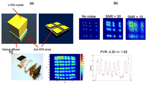
(a) An Anger-logic PET block detector based on light multiplexing. A 2×2 array of large-area high gain APDs were used. (b) Simulated flood maps with different detector SNRs. Only one quadrant for the 8×8 array was simulated due to the symmetry. Significant degradation of the flood maps is observed as the SNR decreases. SNR refers to the ratio of the amplitude of 511 keV photopeak over the RMS noise of the detector when a single crystal is coupled directly to the photodetector. (c) The block detector prototype comprising the LYSO array (crystal dimensions: 2.75×3.0×20.0 mm3), the optical diffuser (9 mm thickness), the APD array and highly compact custom readout electronics. The crystal flood map and 1D profile for peak-to-valley ratio (PVR) analysis are shown. Adapted from [51].
It should be noted that in the work that predicts the resolution limit of 500 μm [36], no effect of the scintillation light output and the detector SNR (i.e. signal of a 511 keV photon over RMS noise) was taken into account. The detector SNR can be measured when an individual crystal is readout individually without any multiplexing. From a practical point of view, however, to resolve an array consisting of 250 μm or 500 μm pitch crystals, it is very likely that either charge multiplexing Fig. (4) or optical multiplexing Fig. (5) is to be employed to reduce the total number of readout channels. Based on the theory of Anger logic positioning scheme [52], the reduced light output and reduced SNR will make two adjacent crystals more difficult to be resolved (i.e. lower PVR), as illustrated by the flood histogram and profile results shown in Figs. (4 and 5). The positioning uncertainty associated with the overlap between two crystals in a flood map ultimately degrades the spatial resolution, which corresponds to an increase of the b factor in the formula (3). As a result, the ultimate spatial resolution achievable might be worse than 500 μm as predicated in [36].
3.3. Compton Scatter and Multiple Interactions within Detectors
A 511 keV photon will interact with crystals and deposit its energy through photoelectric effect (PE) and Compton scatter (CS). If the detector elements are small, scattered photons will usually escape into adjacent crystals before depositing their remaining energy (also known as “multiple interactions”). Multiple interactions occurring between adjacent crystals were found to be a dominant source for the mis-positioning of incoming 511 photons and contribute to the tails of the spatial response function [36, 39, 53,54]. This, in turn, degrades spatial resolution and contrast resolution. For an energy threshold of 350 keV on the summed interaction energies per photon event and a lower energy cutoff of 10 keV per interaction, ~25% of the detected events would be positioned away from the true line of entrance (for an 8×8 array of 1×1×10 mm3 LSO crystals) [39]. The implication is that even though the utilization of a finer crystal pitch could improve the spatial resolution, the increases portion of multiple interactions due to the reduced crystal size diminishes that benefit, while causing additional penalty through the light output loss [39].
In general, the probability of photon scattering is higher for relatively low Z, lower density crystals such as GSO and CZT (see Table 1). The probability of multiple interactions is also significant in higher Z crystals such as LSO, if crystal elements are small [36, 39]. Recent work [36] shows that the percentage of multiple interaction and its impact on the photon positioning are also dependent on the thickness of detectors. For a 0.45 cm thick CZT slab, the fraction of multiple interaction events with respect to the total number of events is 31%; while for a 5.98 cm thick CZT slab, the fraction is 77%. For LSO, the fraction is 27% and 63%, for the thickness of 0.27 cm and 3.65 cm, respectively [36]. The above results indicate that when comparing multiple detector layers made of thin slabs of low Z materials such as Si and CZT against a single thick detector layer made of high Z materials such as LSO, the two configurations might end up having the same fraction of multiple interaction events (i.e., positioning uncertainties) [36]. This implies that low Z materials such as Si and CZT are not necessarily exhibiting inferior performance in terms of the positioning uncertainties when compared to high Z materials such as LSO, provided that they are configured in novel detector geometries.
3.4. High Resolution PET Detector Developments
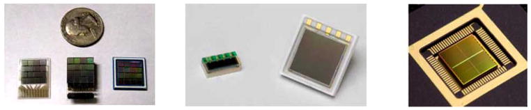
One approach under investigation to address the above challenges is to use semiconductor detector crystals such as CZT or cadmium telluride instead of scintillation crystals [18, 28–31]. In semiconductor crystals, a strong electric field is established across the crystal by applying a relatively large potential difference on the two electrodes (anode and cathode) on either face of a monolithic crystal slab. When an incoming photon interacts with the detector, a cloud of electron-hole pairs are created. The electrons and holes are separated and drift toward opposite faces. The motion of the charge induces signals on the respective electrodes that may be used to extract spatial, energy, and timing information. Thus, unlike scintillation crystals, semiconductor detectors directly sense the ionization signal created by the high-energy photon absorption and do not create, transport, and collect scintillation light. Such direct conversion enables it to exhibit superior energy resolution of ~1.5–3.0% full-width-half-maximum (FWHM) at 511 keV Fig. (6), compared to scintillator-based detectors. In semiconductor detectors, fine pixilation is set by the segmented pattern of charge-collecting electrodes deposited on the crystal slab faces Figs. (1 and 6a), rather than relying on cutting, treating, and assembling many miniscule crystal elements. For instance, to achieve high intrinsic spatial resolution of 500 μm, one deposits the electrodes with a pitch of that matches the desired spatial resolution. The electrodes can be configured in cross-strip or square electrode pixels. In either mode, the detector is able to achieve high-resolution 3-D positioning. Taking a CZT slab of 4×4×0.5 cm3 for example, in the face-on mode where 511 keV photons enter normal to the large face, about eight slabs need to be stacked together (4 cm thickness in total) to achieve high stopping power; in the edge on mode where 511 keV photons enter parallel to the large face as shown in Fig. (1a) high photon detection efficiency can be also achieved. For a 2 cm long LSO crystal (linear attenuation coefficient: 0.86/cm), the intrinsic sensitivity for 511 keV photons is ~82% and for a 4 cm thick CZT detector, it is ~86% (linear attenuation coefficient: 0.50/cm).
Fig. (6).

(a) Picture of a 4×4×0.5 cm3 cross-strip CZT array. For PET, CZT slabs can be configured in the edge-on mode (see Fig. 1) or several slabs can be stacked together in the face-on mode to achieve high stopping power for 511 keV photons. (b) A typical energy spectrum of CZT detector irradiated by 511 keV photons. Energy resolution of 3% FWHM at 511 keV is far superior to that achieved in LSO-based scintillation detectors (~12%), though CZT has relatively poor time resolution. (c) The illustration of 3-D positioning for a cross-trip CZT detector. The C/A ratio (the amplitude of cathode signal over the amplitude of anode signal), and the timing difference between the anode and cathode signals, can be used to determine the interaction position in the direction orthogonal to the electrode planes. These quantities are plotted as a function of collimated beam position between the anode and cathode planes. The error bars denote the extent of the standard deviation for each data point. The width of the collimated photon beam is 1 mm. Adapted from [18, 30].
The principle that a cross-strip CZT detector (4×4×0.5 cm3) extracts 3-D positioning information is illustrated in Figs. (6a and 6c) The spacing of anodes (cathodes) determines the intrinsic spatial resolution along Y (X) direction (see Fig. (1) for the axes definitions); by utilizing the time difference between the signals from the anode and cathode, or, alternately the ratio of peak cathode to anode signals, the system is able to achieve ~ 1 mm resolution along the Z direction, which is better than the thickness of the detector along that direction (5 mm). For instance, if a photon interacts within the detector at a location closer to the anode, a shorter time is required for the electrons to drift to the anode, and accordingly a longer cathode to anode time difference or a smaller cathode to anode peak signal ratio would be measured. Recently, a breast dedicated PET [33] and a box shape small animal PET system [19, 31] based on such CZT detectors are under investigation.
Another approach under investigation to increase light collection efficiency for high-resolution scintillation crystal designs is to read out the larger area side faces of the long and narrow crystals (effective length: 2 cm) rather than the small area ends of the crystals as illustrated in Fig. (7), which substantially improve the crystal aspect ratio and light collection [39]. In this new geometry, with the photodetector surface generally edge-on (parallel) with respect to incoming photons, the average light path to the photodetector is greatly reduced and the light collection is nearly complete (>95%), independent of individual crystal length, width, and surface treatment, as well as origin of the scintillation light [39]. These factors help to achieve high energy and timing resolution in addition to high spatial resolution, without requiring special crystal surfaces or promotion of total internal reflection. In order to accomplish this feat in an array with high crystal packing fraction, very thin PSAPD photodetectors have been manufactured and are configured in between the crystal planes as shown in Fig. (7) [28, 47–49]. With PSAPDs and the edge-on orientation, the annihilation photon interaction depth can be directly measured. Similar to the CZT detectors mentioned above, this detector design is able to achieve 3-D positioning of about 1 mm spatial resolution, while maintaining good energy resolution (~12% FWHM at 511 keV) and time resolution (~ 2 ns).
Fig. (7).

(a) Picture of an edge-on LYSO+PSAPD module designed for breast PET, including scintillation crystals, extra thin PSAPD modules and flex circuit. Each layer comprises two 200 μm thick PSAPD chips mounted on a 50 μm thick flex circuit. The flex circuit delivers bias to each PSAPD and enables readout of the four corner signals for positioning. (b) Picture of the thin module with two PSAPD chips mounted. Each dual-LYSO-PSAPD detector layer is oriented edge-on so that incoming photons encounter a minimum of ~2 cm thick of LSO with directly measured photon interaction depth (~ 1 mm). (c) The crystal flood map of an 8×8 array of 1×1×1 mm3 LYSO crystals without cooling. Adapted from [49].
One potential benefit with novel 3-D positioning photodetectors is that by recording the 3-D coordinates and energy deposition for every interaction, it is possible to use more intelligent positioning algorithms to better estimate the line of entrance of an incoming photon in order to mitigate the positioning errors caused by the multiple interactions [31]. Such positioning algorithms may incorporate the physics of Compton scatter and/or a probabilistic formalism such as maximum likelihood to estimate the first interaction location.
Nevertheless, we would like to point out that these novel designs face challenges in readout electronics developments. Though CZT and LSO-PSAPD detectors under investigation are able to achieve ~ 1 mm spatial resolution in three dimensions while maintain high photon detection sensitivity, the main challenge is that there are thousands of electronic channels required. For example, a dual-panel breast-dedicated PET system based on LSO and PSAPD modules under development will have more than 10,000 individual readout channels Fig. (7). The box-shaped CZT system of an 8×8×8 cm3 FOV will require more than 9000 channels Fig. (1b). On the other hand, the lower gain and poorer detector SNR of APDs and CZT (compared to PMTs) prevent extensive multiplexing to be implemented to reduce the number of readout channels, either with charge multiplexing or light multiplexing. Thus, a key bottleneck in the development of a PET system built from high-resolution 3-D positioning detectors is the development of high-density application-specific integrated circuits (ASICs) that are used to read out hundreds to thousands of densely packed detector channels with complex event hit patterns. Fortunately, there are a number of companies as well as national laboratories that have developed such ASICs nowadays [55–57].
4. DEPTH-OF-INTERACTION (DOI) DESIGN
A well-known problem in PET instrumentation is the parallax error, also known as the depth-of-interaction (DOI) problem, which impacts both the spatial resolution and quantitative studies [24, 58–60]. A PET system typically comprises a circular arrangement of arrays. The interaction of 511 keV photons with long crystal elements at oblique angles, as well as the penetration of 511 keV photons through multiple crystal elements, lead to non-uniform spatial resolution towards the edge of FOV as illustrated in Fig. (8a) for a brain-dedicated PET system with ring geometry. Note that the framework proposed in formula (3) only predicts the spatial resolution around the center of a PET scanner.
Fig. (8).

(a) Illustration of DOI effect on the spatial resolution. For a brain-dedicated PET system of 36 cm diameter bore and crystal length of 20 mm, the intrinsic spatial resolution was studied with a point source shifting from the origin to the edge of FOV. Filtered-back-projection (FBP) was used and for each image, the FWHM of the intensity profile across the point source was analyzed. d1 and d2 are the thickness of the front and back crystal layer, respectively. (b) A configuration between 5/15 (d1/d2) and 10/10 mm is expected to provide the optimum DOI design for achieving uniform spatial resolution across the FOV. The configuration of 0/20 mm implies that only one crystal layer exists. (c) For the breast-dedicated PET system made of CZT detectors (see figure 1a), reconstructed image slices with different DOI resolutions (0, 2, 5 and 10 mm). The simulated spheres of 2 mm diameter are located within a XY plane at the center of the dual-panel system (Z=0). (d) The reconstructed orthogonal-plane (perpendicular to panels) sphere FWHM as a function of DOI resolution. Adapted from [33].
As emphasized in section 2, the use of long crystals is desired for increasing photon detection sensitivity. As a result, for a small diameter PET system or a dual-panel system with closely spaced detectors, on average a higher fraction of photons will interact with scintillation crystals at oblique rather normal angles for a subject of given size. This causes the blurring of the radial component of the spatial resolution that increases with radial position, as illustrated in Fig. (8b). For example, in the brain dedicated PET/MRI system under investigation (PET system diameter: 36 cm, placed outside of a brain RF coil), the spatial resolution shows gradual degradation as a function of the radial distance from the center, as well as the respective thickness of front layer (d1) and back layer (d2). In Fig. (8b) the results indicate that a configuration (front/back: d1/d2) between 5/15 mm and 10/10 mm might be the optimum design for achieving more uniform spatial resolution across the FOV. Note that the 20/0 mm configuration corresponds to a single layer of crystals and has no DOI capability.
Parallax error also occurs for systems of other geometries than a cylindrical ring. For the dual-panel breast system shown in Fig. (1a) a degradation of spatial resolution is also noticeable [33]. In such design, the system has 1 mm intrinsic spatial resolution along both Y and Z directions (see Fig. (1) for the axes definitions). The spatial resolution along the X direction, referred to as the intrinsic DOI resolution, is determined by the cathode spacing and corresponds to the DOI resolution in Figs. (8c and 8d) Under different DOI conditions, the simulation results show that the spatial resolution along the direction perpendicular to the two panels degrades as the DOI resolution increases. The elongated shape of reconstructed spheres along the X direction is due to both the limited tomography configuration (projection angles of less than full 180° coverage) and the limited DOI resolution. Even with DOI resolution being zero, the orthogonal-plane image of spheres still exhibits an elliptical shape as shown in Fig. (8c).
The spatial resolution blurring caused by the DOI capability as described above, can be mitigated if one can determine the photon interaction depth with improved accuracy. How can we incorporate the DOI capability into PET detectors? One could use 3D positioning detectors, either LSO+PSAPD or CZT based detectors examined above. For example, with edge-on PSAPDs configured on the sides of miniscule LSO crystal elements shown in Fig. (7), the segmented crystals are able to achieve 1 mm 3-D intrinsic positioning [47–49]. For CZT detectors, the 3-D positioning capability (~1 mm) may be attained by either the cross-strip design Fig. (6c).
DOI capability can be also introduced for conventional scintillator-based PET detectors. Several DOI designs are summarized below. In general, DOI resolution has two types: discrete DOI and continuous DOI. The former implies that crystals are segmented to independent units (similar to the pixilation of electrodes in CZT detectors) [18]. The latter implies that no physical segmentation is made and DOI is estimated/calibrated using collimated photon beams [26,27, 37]. Meanwhile, it is worthwhile to emphasize the subtle difference between 3-D positioning detectors and 2-D positioning detectors with DOI capability. Standard PET detectors (referred to 2D positioning detectors here) commonly use either light multiplexing in the scintillation crystal array and/or charge multiplexing in the photodetectors, or associated readout circuit to reduce the number of readout channels. As a result, such detectors estimate only the 2-D photon interaction coordinates (x–y) for each event by determining the array crystal closest to the 2-D weighted mean of the readout signals. Consequently, individual interaction coordinates and their energies deposited cannot be determined in the standard PET detector. That said, even though a 2D positioning detector has DOI capability incorporated, it is still fundamentally different from 3D positioning detectors that can measure 3D coordinates of multiple interactions per event.
Here we briefly review five types of DOI designs:
4.1. Multiple Crystal-Photodetector Layers
The design consists of two or more crystal layers each read out by a layer of photodetector(s) [39, 61,62]. As shown in Fig. (9a) the DOI resolution is discrete and determined by the crystal segmentation of each layer. The advantage is that the overall detector performance is not compromised, as there is no optical and electrical interference between two layers. However, the basic drawback of this design is the increasing number of electronic readout channels (2× more) and thus increased development complexity.
Fig. (9).

Illustration of several DOI design concepts for PET. (a) Dual crystal-photodetector(s) layers. (b) Single crystal layer with photodetectors at each end. (c) Phoswich design with two types of scintillation materials. (d) Statistical positioning with a monolithic crystal block. (e) Dual layer crystals with offset positions. (f) Dual layer crystals of mixed shapes.
4.2. Single Crystal Layer + Dual ended Photodetectors
This design employs a single crystal layer read out by two photodetectors on both ends as shown in Fig. (9b). In this way the depth of interaction of the annihilation photon inside the crystal is determined by the difference in the amount of light detected by the two photodetectors [37, 63–65]. For an 8×8 array comprising 1×1×20 mm3 crystal elements, average DOI resolution over all crystals and all depths is ~3.5+/−0.1 mm for an energy threshold E > 350 keV, and ~5.0+/−0.1 mm for E < 350 keV [63]. Such design is also able to extract DOI resolution for even smaller arrays such as 0.5 mm and 0.75 mm crystal pitch [37]. A minor problem about this design is that the light sharing and propagation along the long crystal (~20 mm between the two photodetectors) may result in poor detector performance in terms of energy and/or timing resolution, as well as the positioning non-linearity near the faces of two photodetectors (i.e. nonuniform DOI resolution). In addition, as DOI resolution is directly dependent on the signal differences between two photodetectors, the stability and calibration of detectors, particularly the gain variability between the two photodetectors, remains a challenge. Furthermore, such calibration needs to be performed regularly due to drifting gains of photodetectors.
4.3. Phoswich Design
The phoswich detector comprises two different types of scintillation crystal materials read out from the same photodetector [66,67], as shown in Fig. (9c). DOI capability is realized by pulse shape discrimination based on the fact that the decay time constants of two scintillation materials are different (Table 1). A major challenge of this detector design is that complicated pulse shape discrimination circuits or pulse waveform digitization for each channel, are required to extract the timing difference between pulses originated from two types of materials. Ideally, the DOI resolution should be equal to the thickness of each crystal layer as in DOI design 4.1. However, several factors degrade the DOI capability including the limited decay time difference between two materials (~20–30 ns), the intrinsic timing fluctuation in the signal from each layer and the electronics, multiple interactions involving both layers, as well as the light loss at the interface between two materials of different refractive indices. Nevertheless, such a design achieves adequate performance and a commercial system based on such design is the GE small animal PET scanner (LYSO: 40 ns decay time and GSO: 60 ns decay time, see Table 1) [68].
4.4. Statistical Positioning with Monolithic Crystals
This design extracts the DOI information based on iterative statistical modeling for monolithic crystals [25–27, 69–71]. As shown in Fig. (9d), a monolithic crystal block of relatively large size is read out by either individual photodetector(s) or position sensitive photodetector(s), which can be coupled to either the entrance surface or the exit surface, or both. In essence, the spatial resolution in the cross section of the crystal is obtained in the same manner as that in detectors without DOI capability. While in the DOI direction (the direction along which 511 keV photons enter the crystal), the DOI resolution is determined based on the light output intensity and/or light spread profile which are dependent on the depth of photon interaction. Several algorithms have been developed for this design, including maximum likelihood [69] and mean square error [71]. A recent method, called entry point estimation, shows that by estimating the annihilation photon entry point instead of merely the DOI (i.e. use the information of both the interaction depth and incidence angle), more accurate assignment of LORs could be expected [71]. Despite the simplicity implied by the use of a monolithic crystal layer, the complexity of this design lies mostly in the algorithms and calibrations. For instance, a set of experiments has to be done by irradiating the detector with 511 keV photon beams at a series of known positions and angles of incidence. Moreover, this design is subjected to the degeneracy of positioning near corners and edges of the crystal, where the spatial resolution is inferior compared to that near the center of the crystal. Nevertheless, such design has several attractive benefits beside the DOI capability: first, the use of monolithic crystal avoids complicated crystal cutting and assembly; second, it gets rid of dead area in-between crystal elements and thus increases the photon detection sensitivity; third, no extra optical interface exists and therefore no light loss is introduced as in other designs.
4.5. Dual Layer Crystals of Offset Positions or Mixed Shapes
In this design, two layers of crystals (same material) are involved and are readout by only one layer of photodetectors(s). As the top and bottom layer of crystals have different light output profile, their positions can be extracted. One method is to offset the top layer by half of the crystal pitch with respect to the bottom layer as shown in Fig. (9e) [72]. For illustration only, the top layer is a 9×9 array and the bottom layer is a 10×10 array.
Another design consists of two crystal layers built from crystals of different shapes shown in Fig. (9f). Each layer is built from small modules and each module comprises 8 crystals (4 crystals for each layer). Note that dimension of the base of a triangular crystal is twice that of the pitch of rectangular crystals. Here the light sharing is dependent on the crystal shape. For instance, interactions in the triangles at the top layer form a special light-focusing pattern that enables their differentiation from interactions in the rectangular crystals at the bottom layer. This design provides discrete DOI and does not double the number of photodetectors. It does not require complicated readout electronics that are necessary in a phoswich design. Furthermore, as two layers are made of the same material, no significant light loss occurs at the interface. However, the limitation mainly stays in the complexity and relatively high cost in manufacturing triangular shape crystals, and light loss at interfaces between the two layers.
The preliminary characterization of the triangular crystal design is presented in Fig. (10) for a basic module comprising 8 crystal elements. It is noticed that the crystal flood map is dependent on the configuration of two layers. The performance of crystals at the top layer and the bottom layer was compared in terms of gain (i.e., the position of 511 keV photopeak in the energy spectrum) and energy resolution, after crystal segmentation. A noticeable pattern is that for light produced in the top layer, it suffers from a slight light loss compared when produced in the bottom layer. No significant difference was found in terms of energy resolution. A modulation transfer function (MTF) study was made for both triangular crystals and rectangular crystals and it was found that triangular shape elements do not introduce spatial resolution non-uniformity or artifacts.
Fig. (10).

(a) DOI design using two layers comprising triangular (TRI) and rectangular (RECT) crystal elements. Each module consists of four triangular crystals (top layer) and four rectangular crystals (bottom layer). The two layers produce different light profiles onto the photodetectors and they are coupled using optical grease or epoxy. The picture of individual crystal segments is shown. (b) The flood histograms of a basic module (comprising 8 crystals) are shown for two configurations (rectangular crystals at the top layer or at the bottom layer). The basic module was readout by a 2×2 SiPM array (pixel size: ~3.0 mm) without multiplexing. The gain (in voltage) and the energy resolution FWHM at 511 keV were analyzed after the individual crystals were segmented from the flood histograms. No significant performance difference is observed between crystals in the two layers.
5. TIME-OF-FLIGHT (TOF) PET
Here we briefly overview the history, theory, and recent progress of TOF PET instrumentation. By accurately measuring the arrival time of the two 511 keV annihilation photons, the location of their emission points can be constrained along a LOR between two detector pairs. Though this constraint is not tight enough to avoid the image reconstruction process or improve the spatial resolution, it can significantly increase the SNR in the reconstructed images [73–76]. The image SNR improvement is increased due to the following reason: in a non-TOF PET, the noise from all pixels along a given LOR is correlated; while in TOF PET, the data back-projected along a LOR statistical fluctuations from the data along a LOR contribute to a reduced number of adjacent image pixels, as illustrated in Fig. (11). The framework developed for TOF PET is described in formula (4) [77].
Fig. (11).
Illustration of TOF-PET. (a) In conventional PET, the source of the activity is localized to a LOR between a detector pair (i.e., two measured photons). (b) In TOF-PET, timing information is used to constrain the source of the activity to a segment of the LOR. Adapted from [78].
| (4) |
where Δx is the position error, c is the speed of light, and Δt is the arrival time difference (constrained by the coincidence time resolution), D is the size of the emission source, and G is the effective sensitivity increase. The benefit of TOF increases as the timing resolution decreases. For example, for a time resolution of 500 ps that is currently achievable with fast scintillators and PMTs, Δx is ~7.5 cm long. For an imaging object of 40 cm diameter, the SNR improvement is ~2.3 and G is about 5.3. However, for small animal PET, with the coincidence time resolution of current technologies and small size of subjects (e.g., ~2–5 cm diameter), there is no SNR improvement expected. Therefore, TOF is a technique more beneficial for clinical whole body PET than for small animal PET.
In 1980s, a number of PET cameras incorporating TOF measurement were built based on BaF2 or CsF [73–76, 78] as they are very fast scintillators (see Table 1). However, they were not suitable for PET detectors mainly due to the low light output and low detection efficiency, and the lack of high-quality electronics to perform accurate timing measurements. Over the past few years, there has been renewed interest in TOF-PET [79–82], thanks to the availability of newly developed fast scintillators that also have high light output and high stopping power. Several TOF PET scanners are commercially available, including Philips (crystal: LYSO) [83], Siemens (crystal: LSO) [84] and GE (crystal: LYSO) [85]. All these systems exhibit a best timing resolution of 550–600 ps FWHM, but which degrades versus temperature and count rate [83].
5.1. Fast and High Z Scintillation Materials
The main factor that enables recent TOF PET development is the availability of new scintillator materials, such as LSO, LYSO and LaBr3 crystals. As shown in Table 1, they have light output (good for energy resolution and scatter rejection), fast decay time constant (good for time resolution and random rejection), as well as good stopping power. Besides commercial LYSO-based TOF PET scanners, Philips has recently developed a TOF-PET system based on LaBr3 crystals [86–87], which have a faster decay time and higher light output than LSO or LYSO though it has a lower atomic number. Preliminary characterization indicates that at room temperature and low count rate, an array of 4×4×30mm3 LaBr3 (5% Ce) readout with large-size PMTs could achieve a timing resolution of ~313 ps FWHM and an average energy resolution of ~5.1% FWHM at 511 keV [87], compared to a timing resolution of ~585 ps and an average energy resolution of ~11.5% FWHM at 511 keV for LYSO crystals with the similar electronics used [83]. Furthermore, LaBr3 (Ce) with cerium concentrations other than 5%, as well as other scintillation materials such as CeBr3, and LuI3 (Ce) are also being investigated [78].
Besides the intrinsic properties of materials, other parameters are also important for detector design in TOF PET systems, such as crystal surface treatment and crystal height [88]. In conventional clinical PET detectors, relatively long (e.g., 4×4×20 mm3 LSO crystal pitch) crystals are coupled to the surfaces of PMTs through a light guide. If a scintillation event occurs at the back of one detector but the front of the opposing detector, the difference in propagation time will cause blurring in the measured coincidence timing spectrum [77]. Furthermore, the use of light guide would further degrade the time resolution. In this regard, the detector design in Fig. (9a) appears to be a promising solution, which can have good time resolution (less propagation time within each layer of crystal), good DOI resolution and high sensitivity (total crystal length) at the same time, but at the drawback of increased number of detectors and electronic channel.
5.2. Novel Photodetectors and Electronics
Current commercial TOF-PET systems are all based on PMTs, which has high multiplication gain, superior SNR and good temperature stability. Being available very recently, the silicon-based photomultiplier (SiPM) is considered an attractive photodetector for TOF PET system development [89–93]. Each SiPM pixel, of size ranging from 1 mm to 4 mm, contains thousands of micro-cells with a fine pitch (e.g. 25–100 μm). Each micro-cell operates in Geiger mode. Under ideal conditions, each SiPM will generate a charge signal that is proportional to the number of incoming light photons from a scintillation crystal, with a gain comparable to PMTs (~106). In principle, it is able to resolve single photoelectron peaks. SiPM devices are highly compact and magnetic field compatible. They can also be used for PET/MRI dual modality design, similar to APDs. Recently, two-dimensional arrays of SiPM pixels have become available Fig. (12). Recent studies with these deceives show that a time resolution of 237 ps FWHM and 240 ps FWHM can be achieved for LaBr3 [94] and LYSO [95] crystals (crystal dimensions: 3×3×20 mm3), which is superior to that obtained with PMTs.
Fig. (12).
(left) Designs of 4 × 4 arrays of SiPM devices with ~3.0 mm pitch from SensL, including glass slide, three-sided buttable array and BGA packages. (middle) Designs of a 1 × 4 array (1 mm pixel pitch) and a 2×2 array (3 mm pixel pitch) of SiPM devices from Hamamatsu. (right) A digital SiPM device developed by Philips (a 2×2 array). Active area of each pixel is ~3.8×3.3 mm2. Signal from multiple micro-cells within a pixel are digitally added which reduces the dark count rate and improves SNR. Adapted from [92–93, 96].
In addition, Philips has recently developed digital SiPM technology implemented in CMOS process [96], as shown in Fig. (12). Readout electronics such as analog-to-digital converter (ADC) and time-to-digital converter (TDC) are integrated inside the SiPM chip. The main benefits of the digital SiPM include low dark count rate, high production yield, and improved timing performance. Furthermore, no additional analog readout electronics (e.g. ASICs) are needed. Philips recently reported that the device is able to achieve a time resolution of 170 ps FWHM, for a single LYSO crystal of 3×3×5 mm3 [96].
Despite its promising features, for SiPM-based PET detectors to be deployed in a clinical TOF PET system, there are several concerns to be kept in mind such as significant dead area in-between pixels (fill factor) and adjacent arrays, long term performance stability (i.e., temperature dependency), number of readout channels and cost effectiveness. Due to the increased amount of channels to be readout compared to PMTs, high-performance multiplexing circuits and ASICs with good timing performance are also required.
5.3. Clinical Trials and Performance Evaluation
At the time TOF PET was introduced in the 1980s, PET systems were mainly used for brain and cardiac imaging whereas resolving small lesions and improving SNR were not deemed critical. However, TOF PET has gained more research and clinical attention as PET increases its role in oncology. Several simulation and experimental studies were performed to investigate the performance of whole-body TOF PET systems. Phantom studies with a LYSO-based commercial TOF PET scanner (Philips Gemini TF PET/CT) indicate that TOF information not only increases the lesion detection ability by a SNR gain of 1.4–1.6 (for a 10 mm diameter lesion within 35 cm diameter background), but also reduces the number of iterations required in the image reconstruction [97]. Meanwhile, clinical studies also provide promising results that a TOF PET is able to reveal/define structural details in colon cancer, abdominal cancer and lymphoma [97].
Recently, a LaBr3-based TOF PET system has been investigated [86,87]. The system exhibits inferior performance compared to a LYSO-based scanner in terms of the photon sensitivity and spatial resolution (due to low Z). However, it exhibits a higher NEC rate as defined in formula (1) compared to that of the LYSO-based system. Surti et al conclude that the lower sensitivity of LaBr3 is partially offset by its lower scatter and randoms fractions because it has better energy resolution (~6.5%, LSO: 16% at 511 keV) [86,87]. Note that such improvement is possible with two modifications made: the crystal thickness increases from 20 mm (LYSO) to 30 mm (LaBr3) and the axial FOV increases from 18 cm (LYSO) to 25 cm (LaBr3).
For this promising technique, there are several issues to be further explored. First, the framework proposed in formula (4) might be an over-simplified model to predict SNR improvement in other organs such as brain and heart, where the radioactivity distribution is not uniform. For instance, the activity concentration ratio between myocardium wall and blood pool within the left ventricle is about 4 when fludeoxyglucose (FDG) is used [77]. This might make the achievable SNR less than that as predicated by formula (4). Besides, whether the TOF capability is able to improve SNR and CNR, and then help in imaging small lesions in specific organs (i.e. heart and brain), is an open question. Second, besides evaluating the timing resolution with a single crystal coupled directly to a photodetector, more thorough characterization needs to be done, including the evaluation of the timing performance for a full block detector with light/charge multiplexing scheme in place, if required, as well as the evaluation under various count rate and temperature conditions. For instance, pulse pile up might pose a limit on the achievable time resolution in a real PET system as the count rate increases [83].
CONCLUSIONS
PET technology has not yet reached its performance potential. There are still substantial improvements to be made in terms of photon detection sensitivity, spatial resolution and image quality. An ideal PET system would have high photon detection sensitivity, high spatial resolution, high NEC, good energy resolution and time resolution while maintaining cost-effectiveness. Nevertheless, there are several trade-offs to be made as mentioned in this paper. For instance, for standard 2D-positioning PET detectors, long scintillation crystals would increase the sensitivity but would degrade energy resolution, time resolution and spatial decoding. 3D-positioning PET detector designs based on CZT and PSAPD are attractive solutions to be able to address most of problems, but still face challenges such as large number of readout channels. To be able to push the performance limit of PET systems, efforts in the development of scintillation materials, detectors and readout electronics are required. We believe that advanced instrumentation would help PET enhance its molecular sensitivity in both clinical and small animal research. If successful, PET would be useful in the clinic to visualize and quantify smaller congregations of malignant cells emitting signal in order to help detect earlier signatures of primary or metastatic cancer, for example. In small animal imaging research, such advances would be critical to measure lower concentrations of signal associated with new probes, targets, and assays under study. This enhancement would facilitate deeper probes of disease biology within the cells of living subjects and enable quantification of subtle signatures of molecular-based disease processes.
References
- 1.Gambhir SS. Molecular imaging of cancer with positron emission tomography. Nat Rev Cancer. 2002;2:683–693. doi: 10.1038/nrc882. [DOI] [PubMed] [Google Scholar]
- 2.Nestle U, Weber, Hentschel WM, Grosu AL. Biological imaging in radiation therapy: role of positron emission tomography. Phys Med Biol. 2009;54:R1–25. doi: 10.1088/0031-9155/54/1/R01. [DOI] [PubMed] [Google Scholar]
- 3.Phelps ME. Positron emission tomography provides molecular imaging of biological processes. Proc Natl Acad Sci USA. 2000;97:9226–9233. doi: 10.1073/pnas.97.16.9226. [DOI] [PMC free article] [PubMed] [Google Scholar]
- 4.Rohren EM, Turkington TG, Coleman E. Clinical applications of PET in oncology. Radiology. 2004;231:305–332. doi: 10.1148/radiol.2312021185. [DOI] [PubMed] [Google Scholar]
- 5.Ray P, Pimenta H, Paulmurugan R, Berger F, Phelps ME, Iyer M, Gambhir SS. Noninvasive quantitative imaging of protein-protein interactions in living subjects. Proc Nat Acad Sci USA. 2002;99(5):3105–3110. doi: 10.1073/pnas.052710999. [DOI] [PMC free article] [PubMed] [Google Scholar]
- 6.Luker GD, Sharma V, Pica CM, Dahlheimer JL, Li W, Ochesky J, Ryan CE, Piwnica-Worms H, Piwnica-Worms D. Noninvasive imaging of protein-protein interactions in living Animals. Proc Nat Acad Sci. 2002;99(10):6961–6966. doi: 10.1073/pnas.092022399. [DOI] [PMC free article] [PubMed] [Google Scholar]
- 7.Adonai N, Nguyen KN, Walsh J, Iyer M, Toyokuni T, Phelps ME, McCarthy T, McCarthy DW, Gambhir SS. Ex vivo cell labeling with 64Cu-pyruvaldehyde-bis (N4-methylthi-osemicarbazone) for imaging cell trafficking in mice with positron emission tomography. Proc Natl Acad Sci USA. 2002;99(5):3030–3035. doi: 10.1073/pnas.052709599. [DOI] [PMC free article] [PubMed] [Google Scholar]
- 8.Wang J, Maurer L. Positron emission tomography: Applications in drug discovery and drug development. Curr Top Med Chem. 2005;5(11):1053–1075. doi: 10.2174/156802605774297056. [DOI] [PubMed] [Google Scholar]
- 9.Frangioni JV, Hajjar RJ. In vivo tracking of stem cells for clinical trials in cardiovascular disease. Circulation. 2004;110:3378–3383. doi: 10.1161/01.CIR.0000149840.46523.FC. [DOI] [PubMed] [Google Scholar]
- 10.Cao F, Lin S, Xie X, Ray P, Patel M, Zhang X, Drukker M, Dylla SJ, Connolly AJ, Chen X, Weissman IL, Gambhir SS, Wu JC. In vivo visualization of embryonic stem cell survival, proliferation, and migration after cardiac delivery. Circulation. 2006;113(7):1005–1014. doi: 10.1161/CIRCULATIONAHA.105.588954. [DOI] [PMC free article] [PubMed] [Google Scholar]
- 11.Blasberg RG, Tjuvajev JG. Molecular-genetic imaging: Current and future perspectives. J Clin Invest. 2003;111:1620–1629. doi: 10.1172/JCI18855. [DOI] [PMC free article] [PubMed] [Google Scholar]
- 12.Pither R. PET and the role of in vivo molecular imaging in personalized medicine. Expert Rev Mol Diagnost. 2003;3(6):703–713. doi: 10.1586/14737159.3.6.703. [DOI] [PubMed] [Google Scholar]
- 13.Shah K, Jacobs A, Breakefield XO, Weissleder R. Molecular imaging of gene therapy for cancer. Gene Ther. 2004;11(15):1175–1187. doi: 10.1038/sj.gt.3302278. [DOI] [PubMed] [Google Scholar]
- 14.Luker GD. Special conference of the american association for cancer research on molecular imaging in cancer: Linking biology, function, and clinical applications in vivo. Cancer Res. 2002;62:2195–2198. [PubMed] [Google Scholar]
- 15.Hnatowich DJ. Observations on the role of nuclear medicine in molecular imaging. J Cell Biochem. 2002;87(S39):18–24. doi: 10.1002/jcb.10400. [DOI] [PubMed] [Google Scholar]
- 16.Strother SC, Casey ME, Hoffman EJ. Measuring PET scanner sensitivity: Relating count rates to image signal-to-noise ratios using noise equivalent counts. IEEE Trans Nucl Sci. 1990;37:783–788. [Google Scholar]
- 17.Phelps ME, Huang SC, Hoffman EJ. An analysis of signal amplification using small detectors in positron emission tomography. J Comput Assist Tomogr. 1982;6:551–565. doi: 10.1097/00004728-198206000-00021. [DOI] [PubMed] [Google Scholar]
- 18.Levin CS. New imaging technologies to enhance the molecular sensitivity of positron emission tomography. Proc IEEE. 2008;96:439–467. [Google Scholar]
- 19.Habte F, Foudray AM, Olcott PD, Levin CS. Effects of system geometry and other physical factors on photon sensitivity of high-resolution positron emission tomography. Phys Med Biol. 2007;52:3753–72. doi: 10.1088/0031-9155/52/13/007. [DOI] [PMC free article] [PubMed] [Google Scholar]
- 20.Alessio A, Kinahan P, Cheng P, Vesselle H, Karp J. PET/CT scanner instrumentation, challenges, and solutions. Radiol Clin North Am. 2004;42:1017–1032. doi: 10.1016/j.rcl.2004.08.001. [DOI] [PubMed] [Google Scholar]
- 21.Bao Q, Newport D, Chen M, Stout DB, Chatziioannou AF. Performance evaluation of the inveon dedicated PET preclinical tomograph based on the NEMA NU-4 standards. J Nucl Med. 2009;50:401–8. doi: 10.2967/jnumed.108.056374. [DOI] [PMC free article] [PubMed] [Google Scholar]
- 22.Huisman MC, Reder S, Weber AW, Ziegler SI, Schwaiger M. Performance evaluation of the Philips MOSAIC small animal PET scanner. Eur J Nucl Med Mol Imaging. 2007;34:532–540. doi: 10.1007/s00259-006-0271-7. [DOI] [PubMed] [Google Scholar]
- 23.Townsend DW, Jakoby B, Long MJ. Performance and clinical workflow of a new combined PET/CT scanner. J Nucl Med. 2007;48:437P. [Google Scholar]
- 24.Cherry SR, Sorenson JA, Phelps ME. Physics in nuclear medicine. 3. Philadelphia, PA: Saunders; 2003. [Google Scholar]
- 25.Joung J, Miyaoka RS, Lewellen TK. cMice: a high resolution animal PET using continuous LSO with a statistics based positioning scheme. Nucl Instrum Methods Phys Res A. 2002;489:584–598. [Google Scholar]
- 26.Maas MC, Schaart DR, van der Laan DJ, Bruyndonckx P, Lemaître C, Beekman FJ, van Eijk CW. Monolithic scintillator PET detectors with intrinsic depth-of-interaction correction. Phys Med Biol. 2009;54:1893–1908. doi: 10.1088/0031-9155/54/7/003. [DOI] [PubMed] [Google Scholar]
- 27.Ling T, Lee K, Miyaoka RS. Performance comparisons of continuous miniature crystal element (cMiCE) detectors. IEEE Trans Nucl Sci. 2006;53:2513–2518. [Google Scholar]
- 28.Levin CS, Habte F, Foudray AMK, Zhang J, Chinn G. Impact of high energy resolution detectors on the performance of a PET system dedicated to breast cancer imaging. Phys Med. 2006;21:28–34. doi: 10.1016/S1120-1797(06)80020-7. [DOI] [PubMed] [Google Scholar]
- 29.Levin CS. Primer on molecular imaging technology. Eur J Nucl Med Mol Imaging. 2005;32(2):S325–S345. doi: 10.1007/s00259-005-1973-y. [DOI] [PubMed] [Google Scholar]
- 30.Gu Y, Matteson J, Skelton RT, Deal AA, Stephan EA, Duttweiler F, Gasaway TM, Levin CS. 3-D positioning cross-strip cadmium zinc telluride detector for PET. IEEE Nucl Sci Symp Conf Rec. 2008:3596–3603. [Google Scholar]
- 31.Pratx G, Levin CS. Bayesian reconstruction of photon interaction sequences for high-resolution PET detectors. Phys Med Biol. 2009;54:5073–5094. doi: 10.1088/0031-9155/54/17/001. [DOI] [PMC free article] [PubMed] [Google Scholar]
- 32.James SS, Cherry SR. Simulation study of spatial resolution and sensitivity for the tapered depth of interaction PET detectors for small animal imaging. Phys Med Biol. 2010;55:N63–N74. doi: 10.1088/0031-9155/55/2/N04. [DOI] [PMC free article] [PubMed] [Google Scholar]
- 33.Peng H, Olcott PD, Pratx G, Foudray AMK, Chinn G, Levin CS. Design study of a high-resolution breast-dedicated PET system built from cadium zinc telluride detcetors. IEEE Nucl Sci Symp Conf Rec. 2007:3700–3704. [Google Scholar]
- 34.Moses WW, Derenzo SE. Empirical observation of resolution degradation in positron emission tomographs utilizing block detectors. J Nucl Med. 1993;34:101P. [Google Scholar]
- 35.Levin CS, Hoffman EJ. Calculation of positron range and its effect on the fundamental limit of positron emission tomography system spatial resolution. Phys Med Biol. 1999;44:781–799. doi: 10.1088/0031-9155/44/3/019. [DOI] [PubMed] [Google Scholar]
- 36.Stickel JR, Cherry SR. High-resolution PET detector design: modelling components of intrinsic spatial resolution. Phys Med Biol. 2005;50:179–195. doi: 10.1088/0031-9155/50/2/001. [DOI] [PubMed] [Google Scholar]
- 37.James SS, Yang Y, Wu Y, Farrell R, Dokhale P, Shah KS, Cherry SR. Experimental characterization and system simulations of depth of interaction PET detectors using 0.5 mm and 0.7 mm LSO arrays. Phys Med Biol. 2009;54:4605–4615. doi: 10.1088/0031-9155/54/14/015. [DOI] [PMC free article] [PubMed] [Google Scholar]
- 38.Cherry SR, Shao Y, Tornai MP, Siegel S, Ricci AR, Phelps ME. Collection of scintillation light from small BGO crystals. IEEE Trans Nucl Sci. 1995;42:1058–1063. [Google Scholar]
- 39.Levin CS. Design of a high resolution and high sensitivity scintillation crystal array for PET with nearly complete light collection. IEEE Trans Nucl Sci. 2002;45:2236–2243. [Google Scholar]
- 40.Cherry SR, Shao Y, Siegel S, Silvermad RW, Meadorsl K, Young J, Jones WF, Newport D, Moyers C, Mumcuoglu EU, Chatziioannoul A, Farquhar T, Andreaco M, Paulus M, Binkley D, Nutt R, Phelpsl ME. Micro-PET: a high resolution PET scanner for imaging small animals. IEEE Trans Nucl Sci. 1997;44:1161–1166. [Google Scholar]
- 41.Surti S, Karp JS, Perkins AE, Freifelder R, Muehllehner G. Design evaluation of A-PET: A high sensitivity animal PET camera. IEEE Trans Nucl Sci. 2003;50:1357–1363. [Google Scholar]
- 42.Uribe J, Li H, Xing T, Liu Y, Baghaei H, Wang Y, Aykac M, Ramirez R, Wong WH. Signal characteristics of individual crystals in high resolution BGO detector designs using PMT-quadrant sharing. IEEE Trans Nucl Sci. 2003;50:355–361. [Google Scholar]
- 43.Fontaine R, Belanger F, Cadorette J. Architecture of a dual-modality, high-resolution, fully digital positron emission tomography/computed tomography (PET/CT) scanner for small animal imaging. IEEE Trans Nucl Sci. 2005;52:691–696. [Google Scholar]
- 44.Ziemons K, Auffray E, Barbier R. The ClearPETTM project: Development of a 2nd generation high-performance small animal PET scanner. Nucl Instrum Methods Phys Res A. 2005;537:307–311. [Google Scholar]
- 45.Stickel JR, Qi J, Cherry SR. Fabrication and characterization of a 0.5-mm lutetium oxyorthosilicate detector array for high-resolution PET applications. J Nucl Med. 2007;48:115–121. [PubMed] [Google Scholar]
- 46.Catana C, Wu Y, Judenhofer MS, Qi J, Pichler BJ, Cherry SR. Simultaneous acquisition of multislice PET and MR images: Initial Results with a MR-compatible PET scanner. J Nucl Med. 2006;47:1968–1976. [PubMed] [Google Scholar]
- 47.Levin CS, Foudray AMK, Olcott PD, Habte F. Investigation of position sensitive avalanche photodiodes for a new high-resolution PET detector design. IEEE Trans Nucl Sci. 2004;51:805–810. [Google Scholar]
- 48.Zhang J, Foudray AMK, Olcott PD, Farrell R, Shah K, Levin CS. Performance characterization of a novel thin position-sensitive avalanche photodiode for 1 mm resolution positron emission tomography. IEEE Trans Nucl Sci. 2007;54:415–421. [Google Scholar]
- 49.Lau FWY, Olcott PD, Horowitz MA, Peng H, Levin CS. Noise analysis of LSO-PSAPD PET detector front-end multiplexing circuits. IEEE Nucl Sci Symp Conf Rec. 2007:3212–3219. [Google Scholar]
- 50.Shah KS, Farrell R, Grazioso R, Harmon ES, Karplus E. Positron sensitive avalanche photodiodes for gamma-ray imaging. IEEE Trans Nucl Sci. 2002;49(4):1687–1692. [Google Scholar]
- 51.Peng H, Olcott PD, Spanoudaki V, Levin CS. Can large-area avalanche photodiodes be used for a clinical PET/MRI block detector? IEEE Nucl Sci Symp Conf Rec. 2008:4675–4680. [Google Scholar]
- 52.Anger H. Scintillation camera. Rev Sci Instrum. 1958;29:27–33. [Google Scholar]
- 53.Levin CS, Tornai MP, Cherry SR, MacDonald LR, Hoffman EJ. Compton scatter and x-ray crosstalk and the use of very thin intercrystal septa in high resolution PET detectors. IEEE Trans Nucl Sci. 1997;44:18–24. [Google Scholar]
- 54.Lecomte R, Schmitt D, Lamoureux G. Geometry study of a high resolution PET detection system Using Small Detectors. IEEE Trans Nucl Sci. 1984;31:556–561. [Google Scholar]
- 55.Olcott PD, Levin CS, Tumer T, Clajus M, Cajipe V, Hayakawa S. Preliminary results from a front-end readout ASIC for 1 mm resolution PET systems based upon position sensitive avalanche photodiodes. J Nucl Med. 2006;47(Suppl):1507. [Google Scholar]
- 56.Olcott PD, Levin CS, Cajipe V, Clajus M, Tumer T, Volkovskii A. Evaluation of a new readout ASIC for a 1 mm resolution PET system based upon position sensitive avalanche photodiodes. J Nucl Med. 2007;48(Suppl):135. [Google Scholar]
- 57.Tumer TO, Cajipe VB, Clajus M, Hayakawa S, Vokovskii A. Multi-channel front-end readout IC for position sensitive solid-state detectors. IEEE Nucl Sci Symp Conf Rec. 2006:384–388. [Google Scholar]
- 58.Moses MM, Virador PRG, Derenzo SE. Design of a high-resolution, high-sensitivity PET camera for human brains and small animals. IEEE Trans Nucl Sci. 1997;44(4):1487–91. [Google Scholar]
- 59.Soret M, Bacharach SL, Buvat I. Partial-volume effect in PET tumor imaging. J Nucl Med. 2007;48:932–945. doi: 10.2967/jnumed.106.035774. [DOI] [PubMed] [Google Scholar]
- 60.Phelps ME. PET molecular imaging and its biological applications. New York: Springer; 2004. [Google Scholar]
- 61.Rafecas M, Boning G, Pichler BJ, Lorenz E, Schwaiger M, Ziegler SI. A monte carlo study of high resolution PET with granulated dual layer detectors. IEEE Trans Nucl Sci. 2001;48:1490–1495. [Google Scholar]
- 62.Rafecas M, Boning G, Pichler BJ, Lorenz E, Schwaiger M, Ziegler SI. Inter crystal scatter in a dual layer, high resolution LSO-APD positron emission tomography. Phys Med Biol. 2003;48:821–848. doi: 10.1088/0031-9155/48/7/302. [DOI] [PubMed] [Google Scholar]
- 63.Yang Y, Dokhale PA, Silverman RW, Shah KS, McClish MA, Farrell R, Entine G, Cherry SR. Depth of interaction resolution measurements for a high resolution PET detector using position sensitive avalanche photodiodes. Phys Med Biol. 2006;51:2131–2142. doi: 10.1088/0031-9155/51/9/001. [DOI] [PubMed] [Google Scholar]
- 64.Yang Y, Wu Y, Qi J, James SS, Du H, Dokhale PA, Shah KS, Farrell R, Cherry SR. A prototype PET scanner with DOI-encoding detectors. J Nucl Med. 2008;49:1132–40. doi: 10.2967/jnumed.107.049791. [DOI] [PMC free article] [PubMed] [Google Scholar]
- 65.Moses WW, Derenzo SE, Melchert CL, Manentet RA. A room temperature LSO/PIN photodiode PET detector module that measures depth of interaction. IEEE Trans Nucl Sci. 1995;42–44:1085–1089. [Google Scholar]
- 66.Mosset JB, Devroede O, Krieguer M, Rey M, Vieira JM, Jung JH. Development of an optimized LSO/LuYAP phoswich detector head for the lausanne clearPET demonstrator. IEEE Trans Nucl Sci. 2006;53:25–29. [Google Scholar]
- 67.Seidel J, Vaquero JJ, Green MV. () Resolution uniformity and sensitivity of the NIH ATLAS small animal PET scanner: Comparison to simulated LSO scanners without depth-of-interaction capability. IEEE Trans Nucl Sci. 2003;50:1347–1350. [Google Scholar]
- 68.Levin CS, Zaidi H. PET Clinics: PET Instrumentation and Quantification. 2007;2:125–160. doi: 10.1016/j.cpet.2007.12.001. [DOI] [PubMed] [Google Scholar]
- 69.Ling T, Burnett TH, Lewellen TK, Miyaoka RS. Parametric positioning of a continuous crystal PET detector with depth of interaction decoding. Phys Med Biol. 2008;53:1843–1863. doi: 10.1088/0031-9155/53/7/003. [DOI] [PMC free article] [PubMed] [Google Scholar]
- 70.Maas MC, Van Der Laan DJ, Schaart DR, Huizenga J, Brouwer JC, Bruyndonckx P, Léonard S, Lemaître C, van Eijk CW. Experimental characterization of monolithic-crystal small animal PET detectors read out by APD arrays. IEEE Trans Nucl Sci. 2006;53:1071–1077. [Google Scholar]
- 71.Schaart DR, van Dam HT, Seifert S, Vinke R, Dendooven P, Löhner H, Beekman FJ. A novel, SiPM-array-based, monolithic scintillator detector for PET. Phys Med Biol. 2009;54:3501–3512. doi: 10.1088/0031-9155/54/11/015. [DOI] [PubMed] [Google Scholar]
- 72.Zhang N, Thompson CJ, Togane D, Cayouette F, Nguyen KQ, Zhang N, Thompson CJ, Togane D, Cayouette F, Nguyen KQ. Anode position and last dynode timing circuits for dual-layer BGO scintillator with PS-PMT based modular PET detectors. IEEE Trans Nucl Sci. 2002;49:2203–2207. [Google Scholar]
- 73.Ter-Pogossian MM, Ficke DC, Yamamoto M, Hood JT. Super PETTI: a positron emission tomograph utilizing photon time-of-flight information. IEEE Trans Med Imaging. 1982;1:179–87. doi: 10.1109/TMI.1982.4307570. [DOI] [PubMed] [Google Scholar]
- 74.Wong WH, Mullani NA, Wardworth G, Hartz RK, Bristow D. Characteristics of small barium fluoride (BaF2) scintillator for high intrinsic resolution time-of-flight positron emission tomography. IEEE Trans Nucl Sci. 1984;31:381–386. [Google Scholar]
- 75.Mullani NA, Gaeta J, Yerian K, Wong WH, Hartz RK, Philippe EA, Bristow D, Gould KL. Dynamic imaging with high resolution time-of-flight PET camera TOFPET-I. IEEE Trans Nucl Sci. 1984;31:609–13. [Google Scholar]
- 76.Mazoyer B, Trebossen R, Schoukroun C, Verrey B, Syrota A, Vacher J, Lemasson P, Monnet O, Bouvier A, Lecomte JL. Physical characteristics of TTV03, a new high spatial resolution time-of-flight positron tomograph. IEEE Trans Nucl Sci. 1990;37:778–782. [Google Scholar]
- 77.Budinger TF. Time-of-flight positron emission tomography: status relative to conventional PET. J Nucl Med. 1983;24:73–78. [PubMed] [Google Scholar]
- 78.Moses WW. Recent Advances and Future Advances in Time-of-Flight PET. Nucl Instrum Methods Phys Res A. 2007;580:919–924. doi: 10.1016/j.nima.2007.06.038. [DOI] [PMC free article] [PubMed] [Google Scholar]
- 79.Lewellen TK. Time-of-Flight PET. Semin Nucl Med. 1998;28:268–275. doi: 10.1016/s0001-2998(98)80031-7. [DOI] [PubMed] [Google Scholar]
- 80.Surti S, Karp JS, Muehllehner G, Raby PS. Investigation of lanthanum scintillators for 3-D PET. IEEE Trans Nucl Sci. 2003;50:348–354. [Google Scholar]
- 81.Surti S, Karp JS, Popescu LM, Daube-Witherspoon ME, Werner M. Investigation of time-of-flight benefit for fully 3-D PET. IEEE Trans Med Imaging. 2006;5:529–538. doi: 10.1109/TMI.2006.871419. [DOI] [PubMed] [Google Scholar]
- 82.Moses WW. Current trends in scintillator detectors and materials. Nucl Instrum Methods Phys Res A. 2002;487:123–128. [Google Scholar]
- 83.Surti S, Karp JS. Experimental evaluation of a simple lesion detection task with Time-of-Flight PET. J Nucl Med. 2007;48:471–480. doi: 10.1088/0031-9155/54/2/013. [DOI] [PMC free article] [PubMed] [Google Scholar]
- 84.Jakoby BW, Bercier Y, Conti M. Performance investigation of a time-of-flight PET/CT scanner. IEEE Nucl Sci Symp Conf Rec. 2008:3738–3743. [Google Scholar]
- 85.Kemp B, Nathan M, Rohren E, Peller P, Murphy R, Lowe V. Clinical evaluation of a prototype time-of-flight PET/CT system. J Nucl Med. 2009;50:1513 (abstract). [Google Scholar]
- 86.Surti S, Karp JS, Muehllehner G. Image quality assessment of LaBr3-based whole-body 3D PET scanners: a Monte Carlo evaluation. Phys Med Biol. 2004;49:4593–4610. doi: 10.1088/0031-9155/49/19/010. [DOI] [PubMed] [Google Scholar]
- 87.Daube-Witherspoon ME, Surti S, Perkins A, Kyba CM, Wiener R, Werner ME, Kulp R, Karp JS. The imaging performance of a LaBr3-based PET scanner. Phys Med Biol. 2010;55:45–64. doi: 10.1088/0031-9155/55/1/004. [DOI] [PMC free article] [PubMed] [Google Scholar]
- 88.Ziegler SI, Ostertag H, Kuebler WK, Lorenz WJ, Otten EW. Effects of scintillation light collection on the time resolution of a time-of-flight detector for annihilation quanta. IEEE Trans Nucl Sci. 1990;37:574–579. [Google Scholar]
- 89.Herbert DJ, Moehrs S, D’Ascenzo N, Belcari N, Del Guerra A, Morsani F, Saveliev V. The silicon photomultiplier for application to high-resolution positron emission tomography. Nucl Instrum Methods Phys Res A. 2007;573:84–87. [Google Scholar]
- 90.McElroy DP, Saveliev V, Reznik A, Rowlands LA. Evaluation of silicon photomultipliers: a promising new detector for MR compatible PET. Nucl Instrum Methods Phys Res A. 2007;571:106–109. [Google Scholar]
- 91.Renker D. New trends in photodetectors. Nucl Instrum Methods Phys Res A. 2007;71:1–6. [Google Scholar]
- 92.SensL Technical Note. Available from: http://www.sensl.com.
- 93.Hamamatsu corporation website. Available from: http://www.hamamatsu.com.
- 94.Schaart DR, Seifert S, van Dam HT, de Boer MR, Vinke R, Dendooven P, Lohner H, Beekman FJ. First experiments with LaBr3:Ce crystals coupled directly to silicon photomultipliers for PET applications. IEEE Nucl Sci Symp Conf Record. 2008:3991–3994. [Google Scholar]
- 95.Kim CL, Wang GC, Dolinsky S. Multi-pixel photon counters for TOF PET detector and its challenges. IEEE Nucl Sci Symp Conf Record. 2008:3586–3590. [Google Scholar]
- 96.Philips website. Available from: http://www.research.philips.com/initiatives/digitalphotoncounting.
- 97.Karp JS, Surti S, Daube-Witherspoon ME, Muehllehner G. Benefit of time-of-flight in PET: experimental and clinical results. J Nucl Med. 2008;49:462–470. doi: 10.2967/jnumed.107.044834. [DOI] [PMC free article] [PubMed] [Google Scholar]