Abstract
We synthesized disk-shaped and nano-sized graphene (DSNG) though a novel ion-exchange methodology. This new methodology is achieved by constructing metal ion/ion-exchange resin framework. The morphology and size of the graphene can be modulated by changing the mass ratio of the carbon-containing resin to the cobalt-containing precursor. This is the first time to show that the DSNG formed on the granular transition metal substrate. The DSNG gives a high intensity of photoluminescence at near-UV wavelength of 311 nm which may provide a new type of fluorescence for applications in laser devices, ultraviolet detector UV-shielding agent and energy technology. The emission intensity of the DSNG is thirty times higher than that of the commercial large graphene. Our approach for graphene growth is conveniently controllable, easy to scale-up and the DSNG shows superior luminescent properties as compared to conventional large graphene.
It is well-known from many theoretical and experimental evidences that nanographene with specifically morphologies have excellent properties for broad application prospects1,2,3,4. The applications of graphene have been widely studied4,5,6. The amazing properties of graphene make it a likely candidate to spur on the next revolution in electronics7. However, large-area graphene flakes are not semiconductor because there is no energy gap. But its energy gap can be opened when graphene is shaped up into quasi-one-dimensional structures with narrow widths (<~30 nm), and similar to CNTs, the energy gap of graphene is tunable from 0 to 0.5 eV, depending on the width and crystallographic orientation of the graphene nanoribbon (GNR)2,8. Graphene also touted as the basis for next generation spintronics devices9,10. Arbitrarily shaped finite graphene nanoflakes (GNFs) can lead to large net spin or antiferromagnetic coupling between groups of electron spins. And the spin of GNFs depends on its shape due to topological frustration of the ð-bonds11,12,13. Large area (>100 nm) graphene behaves as conventional single-electron transistors, exhibiting periodic Coulomb blockade peaks. When the size of graphene narrows down to 100 nm, even sub-10 nm, which refer as graphene quantum dots (GQDs), the peaks become strongly nonperiodic, indicating a major contribution of quantum confinement14. The GQDs with sub-10 nm in width remain conductive and reveal a confinement gap of up to 0.8 eV, demonstrating the possibility of molecular-scale electronics based on graphene15,16. Apart from potential applications for the top-down approach to molecular-scale electronics, GQDs also have other unique properties and potential applications in many fields, such as photovoltaic devices4, biological label17, light emitting diodes18, and sensor19.
Although various effective techniques, such as mechanical exfoliation1, oxidation of graphite20, liquid-phase exfoliation21, epitaxial growth22 and thermal decomposition of SiC23 have been developed to produce single-layer or few-layers graphene, the controlled method of preparing nanographene still counts for the top issue24. Han et al.2 used lithography etching technology lithographically patterned graphene nanoribbon (GNR) structures. Tapaszo et al.8 successfully obtained well-defined nanoribbons with widths down to 2.5 nm by applying a constant bias potential (significantly higher than the one used for imaging) and simultaneously moving the STM tip with constant velocity. Campos et al.25 demonstrated anisotropic etching of the single-layer graphene by thermally activated nickel nanoparticles and obtain sub-10-nm nanoribbons. Dai et al.26 developed a route in which multi-walled carbon nanotubes were partially embedded in a PMMA film and then etched the exposed tube walls by argon plasma. The resulting nanoribbons have smooth edges and very narrow width (10–20 nm). Pan et al.27 have developed a hydrothermal route for cutting preoxidized graphene sheets into GQDs (9.6 nm in average diameter) with blue emissions. Lu et al.15 demonstrated the formation of regularly sized graphene quantum dots on Ru (0001) substrate by using C60, which acts as a unique precursor compared to C2H4. Zhuo et al.28 presented a new facile ultrasonic method to prepare GQDs, which exhibited bright PL in a water solution.
To our best knowledge, the disk-shaped and nano-sized graphene (DSNG) has rarely been reported. The arduousness of obtaining DSNG with well-defined shape is the main reason of the poverty in study. Although some techniques, such as chemically derived techniques29, chemical vapor deposition on template30 and lithography etching31 have been reported, however, effective method to produce DSNG with well-defined shape remains elusive. The disk-shaped and nano-sized structure makes the DSNG possess much higher edge density and fringe defects than that of normal graphene sheets, which will contribute to better edge reactivity and defects-mediated properties31,32. The structural defects may give rise to localized electronic states and lead to the magnetic state in DSNG32,33,34. These can offer key advantages in realizing various electron applications via edge chemical functionalization, such as doping.
Recently, graphene based nanomaterial35 are attracting more and more attentions as luminescent nanomaterials due to their unique properties, such as low toxicity, high luminescent, robust chemical inertness and environmentally-friendly.
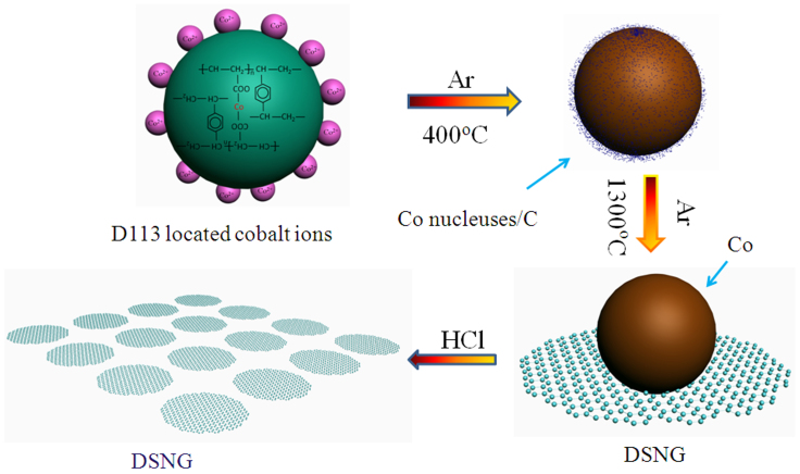
In this paper, we directly synthesized DSNG though a whole new methodology. The new methodology is achieved by constructing metal ion-ion exchange resin framework. The high quality of DSNG was confirmed by atomic force microscopy (AFM), scanning electron microscopy (SEM), Raman, X-ray Diffraction (XRD) and X-ray photoelectron spectroscopy (XPS). Our approach for DSNG growth is actually utmost simple, conveniently controllable and easily scale-up. The synthetic process of the DSNG is shown in Figure 1.
Figure 1. Schematic view of the approach for disk-shaped and nano-sized graphene (DSNG) growth.
Results
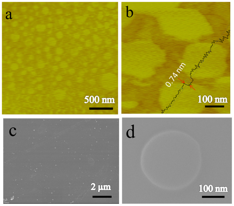
The AFM was used to characterize the material deposited on new-delaminated mica substrate at ambient conditions. It is observed that the material is disk-shaped with the diameter around 200 nm (Figure 2a). The DSNG gave the appearance of the uniform disks. To obtain the morphology and structure of the DSNG, we measured the thickness of the sample by AFM. Figure 2b shows the AFM result that the nano-sized graphene were disk-shaped with the height of 0.74 nm. Figure 2c displays the scanning electron microscope (SEM) of the as-grown DSNG which are well dispersed. As shown in Figure 2d, a perfect disk-like shape can be clearly seen in the SEM micrograph with the size around 200 nm.
Figure 2. Microscopic images of DSNG.
(a). The tapping mode AFM image of the disk-shaped nano-sized graphene (DSNG) prepared at mass ratio of CoCl2·6H2O to D113 resin (RCo/R) of 0.1, (b). a close-up of DSNG, (c). SEM micrograph of DSNG and (d). high resolution SEM micrograph of a DSNG.
The D113 resin exchanged with cobalt ions was heated in tube furnace at 400°C under Ar atmosphere for 2 h, resulting in amorphous powder which was confirmed by the XRD measurements (Figure S3, pattern a). This step is essential in the synthetic process of DSNG, otherwise, no inerratic DSNG is observed (Figure S2). When the sample was further heat treated at 1300°C, the polycrystalline cobalt particles and graphitic carbon formed (Figure S3, pattern b). The Co was removed by HCl treatment for 12 h (Figure S3, pattern c).
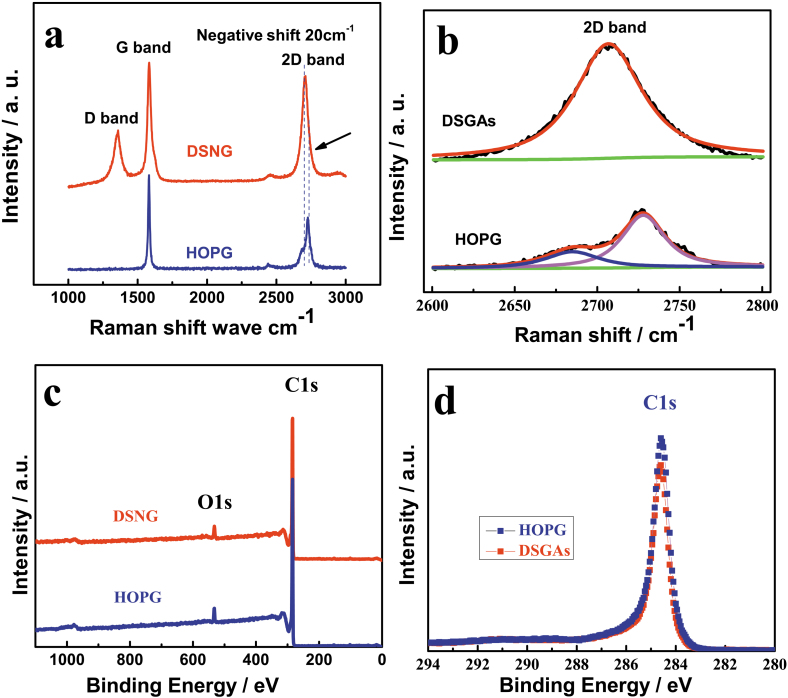
The Raman spectra of the HOPG and DSNG in the range of 1000–3000 cm−1 are shown in Figure 3a. The band observed at about 1577 cm−1 is G band, which corresponds to a splitting of the E2g stretching mode of graphite and reflects the structural intensity of the sp2-hybridized carbon atom. The 1350 cm−1 band (D band), assigned to zone center phonons of K-point phonons of A1g symmetry, characterizes the disordered graphite planes and the defects incorporated into pentagon and heptagon graphitic structures. The minor D band (Figure 3a) in DSNG mainly due to the huge amounts of edges36. The result shows that a significant change in shape and intensity of the 2D band of DSNG compared to HOPG (Figure 3b). The 2D band in the Raman spectrum obtained from HOPG is formed by a two-peak line shape, consisting of two components 2D1 and 2D237. The 2D band in the Raman spectrum of DSNG is a single and sharp peak, formed by one Lorentzian peak38. Notably, the intensities of the 2D band and G band for DSNG are comparable. The 2D position of DSNG is 20 cm−1 shift to lower frequency than that of the HOPG.
Figure 3. Raman and XPS spectra of DSNG.
(a). Comparison of Raman spectra of DSNG (red line) and highly oriented pyrolytic graphite (HOPG) (blue line) at 514 nm, (b). the 2D band in the Raman spectrum obtained from DSNG is formed by one Lorentzian peak, and the HOPG is formed by a two-peak line shape, (c). comparison of XPS spectra of DSNG (red line) and HOPG (blue line) and (d). high-resolution C1s XPS spectra of DSNG (red line) and HOPG (blue line).
X-ray photoelectron spectroscopy (XPS) is a powerful spectroscopic technique that measures the elemental composition, empirical formula, chemical state and electronic state of the elements existed in a material. XPS was used to study the bonding state of carbon atom in the DSNG. The full scan spectra of the DSNG are shown in Figure 3c. The peaks at binding energy of 284.6 eV and 533.15 eV are ascribed to C1s and O1s. The O1s is ascribed to the adsorbed molecular oxygen on the surface of the DSNG and HOPG. The hybridization of carbons influences the properties of a carbon nanomaterial and has implications in its structure. XPS can be used to determine the hybridization of the carbons on the surface of a material, such as graphite and nanodiamond. Graphite is a carbon material consisting of sp2 carbons. Theoretically the XPS of the pure graphite will show a single C1s peak, with a binding energy characteristic of sp2 carbon. Figure 3d shows the detailed C1s XPS spectrum of DSNG (red line) and HOPG (blue line). The main peak at 284.6 eV corresponds to the graphite-like sp2 bonded carbon39. The C1s spectrum of DSNG coincides with HOPG, indicating most of the carbon atoms in DSNG are arranged in a conjugated honeycomb lattice39.
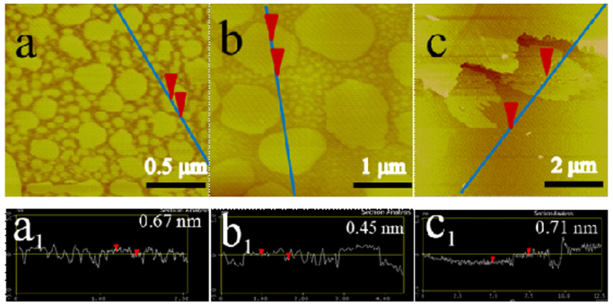
Figure 4 demonstrates that the morphology of the samples is a function of mass ratio of CoCl2.6H2O to D113 resin (RCo/R). It was found that the samples display different geography and size when the RCo/R changes. In the case of the RCo/R = 0.2 and 0.5, there are two kinds of DSNG coexisted with different dimensions of the samples (Figure 4a and 4b). One is bigger and another one is very small. When the RCo/R = 1, the geography of the graphene is inclined to become random (Figure 4c). The AFM height analysis illustrates that the heights of all the samples are between 0.45 nm to 0.71 nm (see Figure 4a1–c1). The Raman spectra (Figure S4) demonstrate that all the samples possess the characteristics of graphene. The XPS spectra (Figure S5) of the samples show that the carbon atoms in the samples are sp2 hybridized carbon in the regular hexagon plane, respectively.
Figure 4. AFM images of the gaphene samples.
The tapping mode AFM images of the graphene samples deposited on new-delaminated mica at ambient condition as a function of mass ratio of CoCl2·6H2O to D113 resin: (a). RCo/R = 0.2, (b). RCo/R = 0.5 and (c). RCo/R = 1. The a1–c1 are the height profiles along the blue lines in (a–c). respectively.
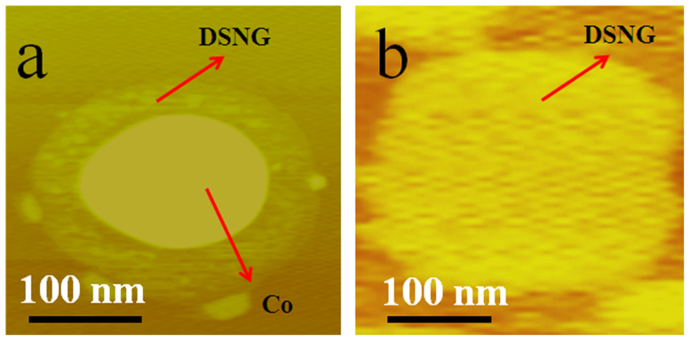
The DSNG is formed by the catalysis of cobalt during the heat treatment which is confirmed by the AFM measurements before and after acid treatment. Figure 5 shows the typical results on a sample prepared in the case of the RCo/R value of 0.1. Figure 5a presents a disk there a Co particle located on the surface of graphene. The peripheral graphene disk is lighter yellow and the Co particle gives darker color, respectively. A flat disk formed after the removal of the Co particle as shown in Figure 5b. The AFM images of the Co on graphene samples with RCo/R = 0.1, 0.2, 0.5 and 1 are shown in Figure S6 and S7.
Figure 5. AFM images of DSNG.
(a). The tapping mode AFM image of the Co/graphene before acid treatment (RCo/R = 0.1) and (b). the tapping mode AFM image of DSNG after acid treatment (RCo/R = 0.1).
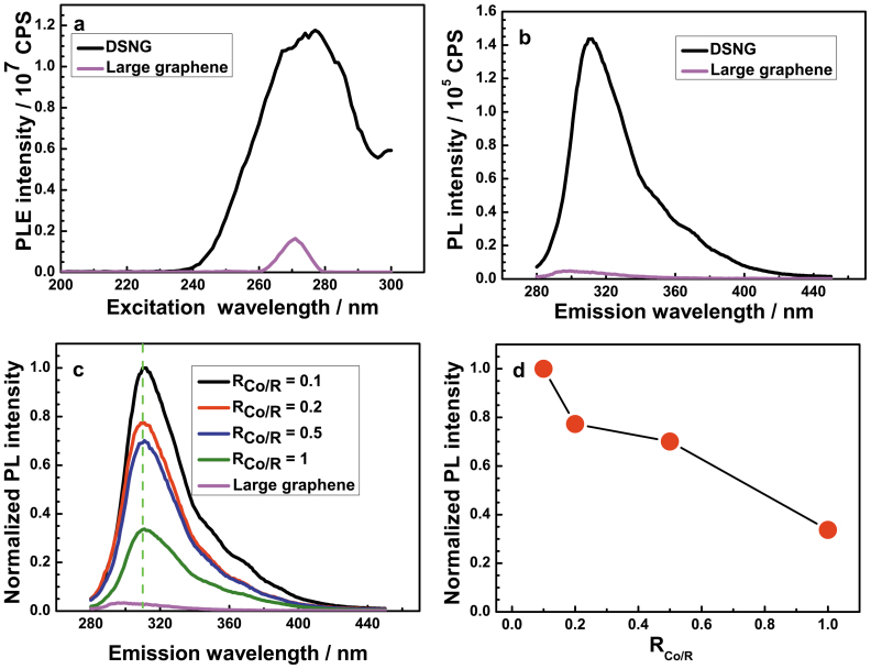
Highly efficient luminescent materials hold the key for applications in optoelectronic devices, biological labeling and sensing40,41,42. Carbon-based nano-materials have been attracting the leading attention as they show high efficiency, stable emissions, chemical inertia, nontoxicity in the physiological condition and no environmental pollution43. With this in mind, we recorded the photoluminescent excitation (PLE) spectrum and PL emission spectrum of DSNG, and the large-area graphene was also tested. A PL emission with high intensity observed from DSNG shows a near-UV wavelength at 311 nm (3.98 eV) under an excitation wavelength of 270 nm (4.62 eV) (Figure 6b). The emission intensity of DSNG is thirty times as high as that of large-area graphene. The enhanced emission indicates that there are more emission active sites. Thus, we expect that the nanostructured DSNG of sp2 configuration of similar size is likely to be responsible for the enhanced near-UV PL. The PLE spectrum for DSNG is shown in Figure 6a. Excitonic features are readily observable between excitation wavelengths of 240 and 295 nm, which represent the absorption energies corresponding to emission of near-UV44. Figure S8 shows the Photograph of suspension of DSNG (1 mg ml−1) in H2O, N-methyl-2-pyrrolidone (NMP), N,N-Dimethylformamide (DMF) and 1,2-Dichloroethane (EDC).
Figure 6. PL spectra of DSNG.
(a). PLE spectra of the DSNG (RCo/R = 0.1) and large-area graphene with the detection wavelength of 311 nm and (b). PL spectra of the DSNG (RCo/R = 0.1) and large-area graphene excited at 270 nm, (c). PL spectra of the nanographene samples with different RCo/R and (d). the relationship between the normalized PL intensity and the RCo/R.
The PL performance of functionalized graphene is related with the size, shape, defects, and preparation method. Table S1 displays different examples of the photoluminescence from functionalized graphene. Figure 6c compares the PL for the graphene samples derived from different RCo/R. All the peaks are in the same near-UV. The emission intensity increases with the decreasing of RCo/R (Figure 6d). The origin of photoluminescence (PL) in these carbon-based nanomaterials is tentatively proposed to be from isolated polyaromatic structures or passivated surface defects43. These results show that the state of the active emission point of the samples are the same. The increase in the emission intensity is mainly due to the increase in the fringe defects which result from the decrease of graphene sheet size. Figure S9 shows the relationship between the normalized PL intensity and the graphene size. The emission intensity decreases with the increase of the graphene size.
Discussion
The synthesis of large area, homogenous graphene on cobalt by chemical vapor deposition CVD method has been reported45,46,47,48. The synthetic mechanism of cobalt catalyzed graphene by CVD is shown as follows. A solid solution of cobalt and carbon is formed when the mixture of H2 and amorphous gaseous carbon (a-C) source is introduced to the hot cobalt film. In the process of cooling down, the high energy carbon atoms in cobalt metal overcome the energy barrier and segregate from the interior of the cobalt film to the surface to form graphene45,47. The graphene grown by CVD on cobalt substrate is extensive,low-defect and homogeneous. Our approach for DSNG growth is schematically illustrated in Figure 1. The D113 resin exchanged with metal ions were carbonized in tubular furnace at 400°C under Ar atmosphere for 2 h. In this process, the cobalt atoms, encapsulated in the exchange sites of the D113 resin, bring together into nucleuses. Simultaneously, the D113 resin began decomposition. After going through a carbonization process, the a-C, derived from the carbonization of the D113 resin, adsorb on the surface of the cobalt nucleuses. The compound is still amorphous solids (Figure S3 pattern a). Next, the compound was then heated to 1300°C for 1 h under Ar atmosphere condition. At this stage, the cobalt nucleuses grow and become polycrystalline cobalt particles with the increase of the temperature (Figure S3, pattern b). The sample was then cooled down to room temperature. In the process of cooling, the carbon atoms diffuse out of the cobalt to the surface, forming the nanographene. These infant nanographenes are expanding outward homogeneously at all orientations, forming a series of inerratic DSNG (Figure 5a).
In conclusion, we reported a novel ion-exchange method to synthesize the DSNG with superior luminescent properties. This is the first example to show that the DSNG formed under the catalysis of the granular cobalt. The morphology and size of the graphene can be modulated by changing the mass ratio of the cobalt-containing precursor to the carbon-containing resin. The DSNG synthesized in this work showed high efficiency in near-UV luminescence which may provide a new type of fluorescence for applications in laser devices, ultraviolet detector UV-shielding agent and energy technology. They may expand the application of graphene-based materials to other fields. Our approach for graphene growth is conveniently controllable, easy to scale-up and readily for applications.
Methods
Preparation of disk-shaped and nano-sized graphene
In a typical preparation, 2.0 g CoCl2.6H2O was dissolved in 200 ml deionized water and 20 g D113 resin was put into the solution (the mass ratio of CoCl2 .6H2O to D113 resin: RCo/R = 0.1). After magnetic stirring for 2 h, the D113 resin loaded with metal ions were rinsed with deionized water for several times and dried in oven at 80°C. Figure S1 shows the typical profile of the ion exchange process of D113 between Co2+ and H+. After carbonized in a tube furnace at 400°C under Ar atmosphere condition for 2 h, the samples were further heat treated in tube furnace at 1300°C for 1 h. The product was post-treated in 3.0 mol L−1 HCl solution for more than 12 h with magnetic stirring to remove cobalt on the surface of the graphene.
The other graphene samples with different morphologies are synthesized by the same steps as mentioned above. In these preparations, 4.0 g, 8.0 g, 20 g CoCl2·6H2O was dissolved in 200 ml deionized water and 20 g D113 resin was put into the solution (RCo/R = 0.2, 0.5 and 1), respectively. After treated by the same steps mentioned above. The graphene samples with different morphologies were obtained.
More details on the experimental section are presented in the Supplementary Information.
Characterizations
The X-ray diffraction (XRD) analysis was performed on a D/Max-III (Rigaku Co., Japan) using Cu Kα radiation, and operating at 40 kV and 30 mA. The 2θ angular regions between 10° and 110° were explored at a scan rate of 5° min−1. The Raman spectroscopic measurements were carried out on a Raman spectrometer (Renishaw Corp., UK) using a He/Ne laser with a wave length of 514.5 nm. The X-ray photoelectron spectroscopy (XPS) measurements were carried out on a XPS apparatus (ESCALAB 250, Thermo-VG Scientific Ltd.). A field emission scanning electron microscope (FESEM,JSM-6330F, JEOL Ltd.) and multimode scanning probe microscope (SPM, Nanoscop IIIa, Digital Instrument Ltd.). PL spectra were measured at room temperature in a FLS920P system (EDINBURGH INSTRUMENTS Ltd.) with a 450 mW xenon arc lamp. All the samples were diluted with DI water to avoid reabsorption; the samples were placed in the cuvettes inside the integrating sphere.
Author Contributions
C.Y.H. and P.K.S. conceived the experiments. C.Y.H. performed the experiments. C.Y.H., P.K.S. and S.P.J wrote the paper. All authors contributed through scientific discussions.
Supplementary Material
Supplementary information
Acknowledgments
This work was supported by the Major International (Regional) Joint Research Project of NNSFC (51210002), the link project of the National Natural Science Foundation of China and Guangdong Province (U1034003), the National Natural Science Foundation of China (21073241), the Specialized Research Fund for the Doctoral Program of Higher Education of China (20110171110024) and Australia Research Council (DP120102325 and DP120104932).
References
- Son Y.-W., Cohen M. L. & Louie S. G. Half-metallic graphene nanoribbons. Nature 444, 347–349 (2006). [DOI] [PubMed] [Google Scholar]
- Han M., Özyilmaz B., Zhang Y. & Kim P. Energy band-gap engineering of graphene nanoribbons. Phys. Rev. Lett. 98, 206805 (2007). [DOI] [PubMed] [Google Scholar]
- Rao C. N. R., Sood A. K., Subrahmanyam K. S. & Govindaraj A. Graphene: the new two-dimensional nanomaterial. Angew. Chem. Int. Ed. 48, 7752–7777 (2009). [DOI] [PubMed] [Google Scholar]
- Zhang Z., Zhang J., Chen N. & Qu L. Graphene quantum dots: an emerging material for energy-related applications and beyond. Energy Environ. Sci. 5, 8869–8890 (2012). [Google Scholar]
- Han T. H. et al. Peptide/Graphene hybrid assembly into core/shell nanowires. Adv. Mater. 22, 2060–2064 (2010). [DOI] [PubMed] [Google Scholar]
- Hwang J. O. et al. Workfunction-tunable, N-doped reduced graphene transparent electrodes for high-performance polymer light-emitting diodes. ACS Nano 6, 159–167 (2011). [DOI] [PubMed] [Google Scholar]
- Westervelt R. M. Graphene nanoelectronics. Science 320, 324–325 (2008) [DOI] [PubMed] [Google Scholar]
- Tapasztó L., Dobrik G., Lambin P. & Biró L. P. Tailoring the atomic structure of graphene nanoribbons by scanning tunnelling microscope lithography. Nat. Nanotechnol. 3, 397–401 (2008). [DOI] [PubMed] [Google Scholar]
- Geim A. K. & Novoselov K. S. The rise of graphene. Nat Mater 6, 183–191 (2007). [DOI] [PubMed] [Google Scholar]
- Hill E. W., Geim A. K., Novoselov K., Schedin F. & Blake P. Graphene spin valve devices. IEEE Trans. Magn 42, 2694–2696 (2006). [Google Scholar]
- Wang W., Yazyev O., Meng S. & Kaxiras E. Topological frustration in graphene nanoflakes: magnetic order and spin logic devices. Phys. Rev. Lett. 102, 157201 (2009). [DOI] [PubMed] [Google Scholar]
- Wang W. L., Meng S. & Kaxiras E. Graphene nanoflakes with large spin. Nano Lett. 8, 241–245 (2007). [DOI] [PubMed] [Google Scholar]
- Pham B. Q. & Truong T. N. Electronic spin transitions in finite-size graphene. Chem. Phys. Lett. 535, 75–79 (2012). [Google Scholar]
- Ponomarenko L. A. et al. Chaotic dirac billiard in graphene quantum dots. Science 320, 356–358 (2008). [DOI] [PubMed] [Google Scholar]
- Lu J., Yeo P. S. E., Gan C. K., Wu P. & Loh K. P. Transforming C60 molecules into graphene quantum dots. Nat. Nanotechnol. 6, 247–252 (2011). [DOI] [PubMed] [Google Scholar]
- Ritter K. A. & Lyding J. W. The influence of edge structure on the electronic properties of graphene quantum dots and nanoribbons. Nat. Mater. 8, 235–242 (2009). [DOI] [PubMed] [Google Scholar]
- Fan L. & Zhang M. Electrochemically generated highly fluorescent graphene quantum dots as a biological label for stem cells. ECS Meeting Abstracts 1201, 1248–1248 (2012). [Google Scholar]
- Bonaccorso F., Sun Z., Hasan T. & Ferrari A. C. Graphene photonics and optoelectronics. Nat. Photon. 4, 611–622 (2010). [Google Scholar]
- Wang L.-J. et al. A graphene quantum dot with a single electron transistor as an integrated charge sensor. Appl. Phys.Lett. 97, 262113 (2010). [Google Scholar]
- Wei Z. et al. Nanoscale tunable reduction of graphene oxide for graphene electronics. Science 328, 1373–1376 (2010). [DOI] [PubMed] [Google Scholar]
- Hernandez Y. et al. High-yield production of graphene by liquid-phase exfoliation of graphite. Nat. Nanotechnol. 3, 563–568 (2008). [DOI] [PubMed] [Google Scholar]
- Li X. et al. Large-area synthesis of high-quality and uniform graphene films on copper foils. Science 324, 1312–1314 (2009). [DOI] [PubMed] [Google Scholar]
- Berger C. et al. Electronic confinement and coherence in patterned epitaxial graphene. Science 312, 1191–1196 (2006). [DOI] [PubMed] [Google Scholar]
- Wei D. & Liu Y. Controllable synthesis of graphene and its applications. Adv. Mater. 22, 3225–3241 (2010). [DOI] [PubMed] [Google Scholar]
- Campos L. C., Manfrinato V. R., Sanchez-Yamagishi J. D., Kong J. & Jarillo-Herrero P. Anisotropic etching and nanoribbon formation in single-layer graphene. Nano Lett. 9, 2600–2604 (2009). [DOI] [PubMed] [Google Scholar]
- Jiao L., Zhang L., Wang X., Diankov G. & Dai H. Narrow graphene nanoribbons from carbon nanotubes. Nature 458, 877–880 (2009). [DOI] [PubMed] [Google Scholar]
- Pan D., Zhang J., Li Z. & Wu M. Hydrothermal route for cutting graphene sheets into blue-luminescent graphene quantum dots. Adv. Mater. 22, 734–738 (2010). [DOI] [PubMed] [Google Scholar]
- Zhuo S., Shao M. & Lee S.-T. Upconversion and downconversion fluorescent graphene quantum dots: ultrasonic preparation and photocatalysis. ACS Nano 6, 1059–1064 (2012). [DOI] [PubMed] [Google Scholar]
- Long D. et al. Fabrication of uniform graphene discs via transversal cutting of carbon nanofibers. ACS Nano 5, 6254–6261 (2011). [DOI] [PubMed] [Google Scholar]
- Son M., Lim H., Hong M. & Choi H. C. Direct growth of graphene pad on exfoliated hexagonal boron nitride surface. Nanoscale 3, 3089 (2011). [DOI] [PubMed] [Google Scholar]
- Cong C. X. et al. Fabrication of graphene nanodisk arrays using nanosphere lithography. J. Phys. Chem. C 113, 6529–6532 (2009). [Google Scholar]
- Yazyev O. V. & Helm L. Defect-induced magnetism in graphene. Phy. Rev. B 75, 125408 (2007). [Google Scholar]
- Palacios J. J., Fernández-Rossier J. & Brey L. Vacancy-induced magnetism in graphene and graphene ribbons. Phy. Rev. B 77, 195428 (2008). [Google Scholar]
- Lehtinen P. O., Foster A. S., Ma Y., Krasheninnikov A. V. & Nieminen R. M. Irradiation-induced magnetism in graphite: a density functional study. Phy.l Rev. Lett. 93, 187202 (2004). [DOI] [PubMed] [Google Scholar]
- Loh K. P., Bao Q., Eda G. & Chhowalla M. Graphene oxide as a chemically tunable platform for optical applications. Nat. Chem. 2, 1015–1024 (2010). [DOI] [PubMed] [Google Scholar]
- Banhart F., Kotakoski J. & Krasheninnikov A. V. Structural defects in graphene. ACS Nano 5, 26–41 (2010). [DOI] [PubMed] [Google Scholar]
- Nemanich R. & Solin S. First- and second-order Raman scattering from finite-size crystals of graphite. Phy. Rev. B 20, 392–401 (1979). [Google Scholar]
- Graf D. et al. Spatially resolved raman spectroscopy of single- and few-layer graphene. Nano Lett. 7, 238–242 (2007). [DOI] [PubMed] [Google Scholar]
- McFeely F. R. et al. X-ray photoemission studies of diamond, graphite, and glassy carbon valence bands. Phy. Rev. B 9, 5268–5278 (1974). [Google Scholar]
- Gupta V. et al. Luminscent graphene quantum dots for organic photovoltaic devices. J. Am. Chem. Soc. 133, 9960–9963 (2011). [DOI] [PubMed] [Google Scholar]
- Zhang Y., Mori T., Niu L. & Ye J. Non-covalent doping of graphitic carbon nitride polymer with graphene: controlled electronic structure and enhanced optoelectronic conversion. Energy Environ. Sci. 4, 4517–4521 (2011). [Google Scholar]
- Mei Q. & Zhang Z. Photoluminescent graphene oxide ink to print sensors onto microporous membranes for versatile visualization bioassays. Angew. Chem. Int. Ed. 51, 5602–5606 (2012). [DOI] [PubMed] [Google Scholar]
- Mei Q. et al. Highly efficient photoluminescent graphene oxide with tunable surface properties. Chem. Commun. 46, 7319–7321 (2010). [DOI] [PubMed] [Google Scholar]
- Xin G. et al. Tunable photoluminescence of graphene oxide from near-ultraviolet to blue. Mater. Lett. 74, 71–73 (2012). [Google Scholar]
- Ramón M. E. et al. CMOS-compatible synthesis of large-area, high-mobility graphene by chemical vapor deposition of acetylene on cobalt thin films. ACS Nano 5, 7198–7204 (2011). [DOI] [PubMed] [Google Scholar]
- Bhaviripudi S., Jia X., Dresselhaus M. S. & Kong J. Role of kinetic factors in chemical vapor deposition synthesis of uniform large area graphene using copper catalyst. Nano Lett. 10, 4128–4133 (2010). [DOI] [PubMed] [Google Scholar]
- Ago H. et al. Epitaxial chemical vapor deposition growth of single-layer graphene over cobalt film crystallized on sapphire. ACS Nano 4, 7407–7414 (2010). [DOI] [PubMed] [Google Scholar]
- Liu N. et al. Universal segregation growth approach to wafer-size graphene from non-noble metals. Nano Lett. 11, 297–303 (2011). [DOI] [PubMed] [Google Scholar]
Associated Data
This section collects any data citations, data availability statements, or supplementary materials included in this article.
Supplementary Materials
Supplementary information


