

Abstract
Cross strip and cross delay line readout microchannel plate detectors in 18 mm, 25 mm and 40 mm active area formats including open face (UV/particle) and sealed tube (optical) configurations have been constructed. These have been tested with a field programmable gate array based electronics for single event encoding. Using small pore MCPs (6 μm) operated in a pair, we achieve gains of >1 × 10⁶ which is sufficient to provide spatial resolution of ~17 μm FHWM with the 18 mm and 40 mm cross strip readouts. New cross strip electronics can process high output event rates (> 4 MHz) with high spatial resolution, and self triggered event timing accuracy of ~1.5 ns for sealed tube XS optical sensors. A peak quantum efficiency of between 13% and 19% at 500 nm has been achieved with SuperGenII photocathodes with response from 400 nm to 900 nm for both cross strip and cross delay line sealed tubes. Local area counting rates of up to 40 kHz (100μm spot) have been attained with XS sealed tubes, along with image linearity and stability to better than 50 μm. 25mm cross delay line tubes achieve ~50 μm resolution and > 2 MHz output event rates.
Keywords: Microchannel Plates, High Resolution Imaging, Photon Counting
1.INTRODUCTION
We have implemented microchannel plate (MCP) imaging photon counting detector schemes1-8 for uses in many fields. The majority of these devices employ either a Cross Strip (XS) anode or Cross Delay Line (XDL) anode for position and time determination for detected events. Two types of device have been constructed, open face detectors for use in high vacuum applications, and sealed tubes with high efficiency, proximity focus SuperGenII 9 photocathodes for optical sensing. The XS anode uses charge division, and centroiding of microchannel plate charge signals detected on two orthogonal layers of sense strips to encode event X-Y position, and event times. The cross delay line anode uses two orthogonal layers with serpentine conductors to encode event positions by differences in the signal arrival times at opposite ends of the serpentine delay lines. The XDL MCP sealed tubes have been made with 25mm format and SuperGenII photocathodes achieving ~15% peak QE. The spatial resolution is ~50 μm FWHM, and event rates of more than 2 MHz can be accommodated with event time tagging to 20 ns using a clock reference, or to ~100 ps when a separate time to digital converter is used. MCP detectors with XS readout can reach values below 10 μm FWHM 5-7, while the timing accuracy of the event detection can be as low as ~100 ps FWHM 2,3. However, the gain required for XS readouts is an order of magnitude lower than other high resolution readouts, such as the XDL8. This substantially increases the local counting rate capabilities and the overall lifetime. Open face XS detector formats of 22 mm and 50 mm have been built using pairs of 6 μm microchannel plates. High speed FPGA based electronics has allowed us to achieve ~17 μm spatial resolution with the 22 mm XS open face detector, and output event rates of ~4 MHz. Sealed tube 22 mm XS detectors have also demonstrated good spatial resolution (< 25 μm FWHM), image linearity and local counting rate capability (40 kHz in a 100 μm spot), with event timing of 1 ns using the new electronics scheme. Background rates are dominated by the thermionic noise of the red sensitive photocathodes. These detector systems may be a significant enabling technology for several important applications, high-speed adaptive optics, astronomy of transient and time-variable sources, and optical metrology. Both our XS and XDL detectors are finding uses in three-dimensional imaging, time resolved astrophysical observations of dynamic objects4, biological single-molecule fluorescence lifetime microscopy1,2, optical and infrared tomography, hybrid mass spectrometry and neutron imaging.
2.CROSS STRIP AND CROSS DELAY LINE DETECTOR SYSTEMS
Cross Strip (XS) and cross delay line (XDL) anodes are physically similar to each other, however they obtain positions of photon events differently. XS works by determination of the charge centroid across several strips, XDL uses the difference in pulse arrival times at the ends of a serpentine conductor to deduce the event position. Fig. 1. shows an overview of the components and functionality of an XS MCP detector. In both devices the incoming photons either produce a photoelectron at the MCP input (open face), or from a photocathode deposited on the inside of the window or on the MCP (sealed tube devices). The photoelectron is then multiplied within the pores of a microchannel plate stack and the resulting electron cloud is accelerated towards, and is collected on, two orthogonal sets of metal electrodes that form the anode. To ensure that an accurate event centroid position is achieved the size of the electron cloud has to be optimized10,11 so that the charge impinges on several neighboring periods of the anode pattern. The XS anode (Fig. 2) is made with layers of metal and glass insulator on a ceramic substrate, producing two sets of strips in orthogonal directions. The top and bottom layers each have 50% of the exposed area, and are thus used to collect the charge from the MCPs equally. Potential crosstalk between the two orthogonal sets of electrodes is reduced by having a set of grounded strips directly below the upper strip electrodes. The pattern period for typical XS anode designs is ~0.7 mm for both the upper and lower conductor strips. The distance between the XS anode and the MCP stack is typically ~2.5 mm, and is determined by the charge cloud spread for the chosen MCP configuration. The individual anode strips are connected to the back side of the anode with hermetically sealed vias. These are connected by a “fan out” to a pad pattern for a standard signal connector. The preamplifier electronics can then be easily connected at the back side of the anode to achieving the best noise characteristics and preserve timing properties.
Figure 1.

A functional schematic diagram of a sealed tube detector with a window, MCP pair and cross strip anode.
Figure 2.

50 mm format cross strip anode on a ceramic substrate. Both upper and lower fingers each receive 50% of the charge input.
In the case of the XDL anode the electrodes for each axis form a continuous serpentine conductor across the whole anode. The layers and interstitial ground plane are essentially the same otherwise. Only four contacts are used, two for each end of the individual axes, allowing the pulse arrival times at the ends of the serpentines to be extracted. Typical serpentine periods are of the order 0.6mm, and these anodes are mounted about 6 mm behind the MCP stack.
Fabrication of XS and XDL anodes is low outgassing, refractory, and accommodates being put into sealed tube ultra high vacuum devices. XS anodes have been fabricated in a variety of sizes and shapes up to 50 mm format, and XDL anodes up to 105 mm have been constructed. XS anodes have been utilized in three detector configurations. One is a sealed tube device (Fig. 3) with a 22 mm XS anode, another is an open face detector with a 22 mm XS anode mounted on a vacuum flange (Fig. 5), and the third is an open face detector with a 50 mm XS anode (Fig. 6). 22 mm XS anode sealed tubes (3 ea) were built by Photonis utilizing the 18 mm active area Photonis standard tube design window and brazed body, which is a good match to the 22 mm XS anode readout. The tube window is 7056 glass with a SuperGenII photocathode on the interior surface. Photoelectrons emitted from the cathode are accelerated over a < 200 μm gap to the MCP stack. The MCPs are 25 mm, 6 μm pore, 80:1 length-to-diameter ratio (L/d) low resistance MCP pairs. The 29 mm XDL anode sealed tubes (2 ea) were also built by Photonis, but in this case the enclosure accommodates a 25 mm active area and the MCPs are 33 mm, 10 μm pore, 60:1 L/d MCPs in a stack of three.
Figure 3.

18 mm sealed tube MCP detector with a 22 mm XS anode and SuperGenII photocathode in housing with preamps.
Figure 5.

18 mm active area MCP detector with a 22 mm cross strip anode mounted in a vacuum flange with electronics.
Figure 6.

40 mm active area MCP detector with a 50 mm cross strip anode mounted in a vacuum flange with electronics behind.
The open face XS detectors (Figs, 5, 6) are mounted into conflat flanges. The RD20 preamplifier boards that amplify the strip charge signals are mounted directly to the flanges. The MCPs are used in a pair in these detectors, and each have MCPs with 6 μm pores with 80:1 L/d. These “demountable” detectors serve as a testbed for development of firmware encoding algorithms, and for the initial testing of performance capabilities prior to sealed tube implementation, but are also useful in some applications for direct detection of particles, UV and neutrons.
3. EVENT POSITION AND TIME ENCODING ELECTRONICS
Determination of event positions on XS anodes requires the electronics to process event signals and calculate the centroid of the electron charge cloud distribution 12,13,14 to a small fraction of the anode period 6,7. In the parallel cross strip electronics configuration (PXS) scheme each strip on the anode (32 X and 32 Y for the 22 mm XS anode) is connected to a preamplifier channel on a 32 channel ASIC, (preshape-32, RD20 from Rutherford Appleton Laboratory and Imperial College London). Two RD-20 ASICs are used on each preamplifier board (Fig. 7) to accommodate 64 channels per board. The unipolar output signals have ~40 ns rise time, and ~250 ns fall time (conversion gain of 0.72 mV/1000e−) and we achieve noise of <1500 electrons rms when attached to the cross strip anodes (Fig. 3). Amplified signals are buffered to drive the cable to the ADC (Fig. 8) and are continuously digitized by 12 bit analog to digital converters (ADCs, Analog Devices ADS5271) operated at 50 MHz sample rate. The digital sample streams are then fed into an FPGA (Xilinx Virtex5) using a LVDS serial transfer at 300MHz. All the event filtering and processing is accommodated in the FPGA in parallel, giving us maximum flexibility in signal algorithms. The ADCs are implemented on a multilayer board that is directly connected to the Xilinx Virtex5 FPGA board (Fig. 8), and a daughterboard allows the FPGA to perform parallel data transmission to a standard PCI digital interface. The Virtex5 FPGA has the appropriate number of input lines and gates and was selected due to its high speed and versatile output configurations. FPGA firmware has been formulated to digitally filter the pulse shape to extract pulse peak information. Data is then passed to algorithms that use the strip charge data to derive the event centroid position and time for both X and Y axes. The events are then buffered before being transferred to a computer as an event list of X, Y and T.
Fig. 7.

18mm XS sealed tube housing with the RD20 amplifier board mounted.
Figure 8.

“PXS” event encoding electronics. 64 channel ADC (50 Msps, 12 bit) on the left, passing data to a Virtex 5 XILINX FPGA on the right. Event data (XYT) is passed to a host computer by the FPGA daughterboard which is connected to a PC DIO card.
The high speed operation of the PXS data processing is accommodated by fully parallel continuous sampling. The PXS electronics simultaneously processes signals on all channels (32 × 32) of cross strip readout (22 mm). Event processing begins when the signal on one or several channels exceeds the predetermined slew threshold, thus establishing a self-triggered configuration. The set of digitized values from the triggered strip channels is passed to the FPGA-peak detection logic. The accuracy of peak detection is improved by filtering the digitized waveforms with “finite impulse response” (FIR) filtering13,14. This is a pipeline process, where earlier samples are retained until clocked out of the algorithm. Event processing algorithms use the output of the digital filters to calculate the peak value of the digitized signal and its temporal position and store the 64 outputs at event rates up to 10 MHz. The timing of the event can be calculated with a ~1 ns accuracy with digital implementation of interpolating algorithms (e.g. digital Constant Fraction Discrimination). The PXS FPGA has been used for considerable firmware development to calculate the event X and Y centroid positions, including the accommodation for pedestal, offsets, amplifier gain nonlinearity, and fixed pattern noise correction. Ongoing work is directed at refining the firmware algorithms to accommodate 2 or more closely spaced events in time on the output channels, and determine how to detect and remove spatial collisions. Detailed results of the system operation are discussed in the following sections.
The electronics event encoding scheme for the XDL anodes is substantively different than that for the XS anodes. To accommodate the fast (<5ns) signals from both ends of the XDL anode delay lines in each axis we use four fast amplifier channels (MAR6 and MAR8) with bandpass filters (~100 MHz) to obtain good fidelity timing signals. At the same time we provide a charge amplifier for each axis to enable encoding of the individual event amplitudes. The fast amplified “start” and “stop” signals are transmitted to a Time to Digital converter (TDC) (Fig. 9) where the arrival times are sensed by a constant fraction discriminator. Differences in the pulse arrival times for the ends of each axis are digitized and passed to a FPGA which outputs the X, Y, pulse amplitude and time data to a parallel interface in a PC. The minimum processing time for individual events is about 140 ns with this system, and it can be used for a variety of XDL anode sizes and end to end delay times. Time stamping of events to ~20 ns is established using the internal clock reference. Much better timing is possible by using two TDC units, where the second unit is used to measure the time of the event in relation to a reference pulse (eg. Laser), rather than encoding the centroid of the event position. Timing resolution in this mode is ~50 ps.
Figure 9.

Four channel TDC for XDL anode readout, includes FPGA for processing of event arrival times to output event positions and event arrival times. Event data (XYT) is passed to a host computer with a PC DIO card.
4.CROSS STRIP DETECTOR PERFORMANCE
The performance of the XS detectors (Figs. 3, 5, 6) using the 22 mm and 50 mm XS anodes with the PXS readout electronics, has been evaluated. Evaluations include the spatial resolution, image distortion, uniform illumination fixed pattern noise, gain and gain uniformity, pulse amplitude distribution, background event rates, event time tagging accuracy, and the local and global event rate processing limits. For the sealed tubes LED sources and a 660 nm pulsed laser were used, and for the open face detectors UV (185 nm) was used. The same type of electronics was used for all the devices (2 sets for the larger 40 mm detector), however since much of the functionality is determined by the firmware algorithms used, we have employed different versions of the event encoding routines. The ability to conveniently change the firmware and processing algorithm parameters to accommodate specific performance requirements, without having to change the physical electronics layouts, is of great advantage and convenience in optimization of performance parameters.
4.1. XS Detector Event Detection and amplification
The measured quantum efficiency of the sealed tube 22 mm XS detectors with “SuperGenII” photocathodes is shown in Fig. 10. The quantum efficiency peaks in the range 13% to 16% at ~500 nm and extends out to 900 nm in the red, as low as 400 nm in the blue and is a typical response curve for “SuperGenII” photocathodes. The gain and pulse height distributions for one of the sealed tube detectors is shown in Fig. 11 and has been tested up to about 1.5 × 10⁶. 80v was applied across the cathode to MCP gap, and 100v across the MCP to anode gap. The peaking of the pulse height distributions is indicative of gain saturation and uniformity, and is confirmed by gain uniformity maps. All three tubes have very similar gain characteristics. The 40 mm and 18 mm open face detectors (Figs. 4, 5) operate at slightly lower MCP bias voltages because the MCP stacks have not been scrubbed to stabilize the gain. However, the general gain and pulse amplitude characteristics are very similar. Most detector tests reported in this paper were acquired with MCP gains in the range 5 × 10⁶ to 1 × 10⁶.
Figure 10.
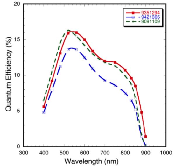
Quantum efficiency for three SuperGenII photocathodes in 22 mm cross strip anode sealed tubes.
Figure 11.

Pulse height distributions at several gains for one of the 22 mm cross strip tubes (6 μm pore MCPs).
Figure 4.

25 mm sealed tube MCP detector with XDL anode and SuperGenII photocathode in housing for SALT-BVIT.
4.2. XS Detector Imaging Characteristics
Much of the optimization has taken place using the open face 22 mm XS and 40mm XS detectors because they are able to be accessed and adapted easily for assessment of the imaging performance. A section of an image taken with the 22 mm XS detector using a uniform illumination of UV light (185 nm lamp) is shown in Fig. 12. The grid pattern is a 20 line per inch metal mesh with 52μm wires placed in contact with the MCP surface. The grid is hard to keep flat so is not a precise tool for distortion measurement but is a good guide for position encoding algorithm development. Visible features such as dark spots are caused by defects on the mesh and MCPs. Faint hexagonal features are also seen, which correspond with the multifibers of the MCP15. Distortions of the MCP pore shape at the multifiber boundaries cause slight variations in the MCP gain and deflect the charge cloud trajectory causing this effect. However, the effect is now minimal as a result of considerable advances in MCP fabrication technology15. Some faint residual “striping” in Y is due to strip to strip charge modulation that has not been fully corrected by the centroid algorithm. The spatial resolution of the detector can be derived from the edge sharpness of the grid wire shadows. Fig. 13 shows the spatial resolution with the 22 mm XS detector at several MCP gain values. Spatial resolution of about 17 μm FWHM is achieved at an MCP gain of 1.4 × 10⁶ which is significantly better than many other devices operating at much higher MCP gain. The background rate of both 22 mm and 40 mm the open face detectors is ~ 0.3 events sec−1 cm−2, which is typical for standard MCPs in this configuration.
Figure 12.

UV illuminated section of an image using the 22 mm XS detector (Fig. 5), showing a grid (1.25 nm period, 52 μm wires.)
Figure 13.

Spatial resolution (FWHM) of the open face XS 22 mm detector as a function of the MCP gain.
In the case of the 22 mm sealed tube XS detectors we project an optical image of a pinhole mask onto the photocathode to assess the spatial resolution and image linearity. A typical image is shown in Fig. 14 using a 1 × 1 mm spaced array of 10 μm diameter spots recorded in a 4096 × 4096 pixel image. The overall image deviations are less than 50 μm except at the very edge of the field of view which is affected by the edge fields of the MCP mounting structure. Histograms the of the pinhole image point spread functions allow us to measure the FWHM spatial resolution. The resolution improves with signal to noise ratio as the MCP gain increases, and reaches about 30 μm for gains above 1 × 10⁶. This can be compared with the image of a small hotspot that is seen in the image which is a result of an emitting spot on the front of the MCP stack. This hotspot reaches a minimum size of about 25 μm at above 1 × 10⁶. The latter value shows that the resolution of the XS readout and electronics is better than the projected spot image data. The principal determinant of the sealed tube spatial resolution in this case is the cathode proximity gap (~200 μm with a ~110v bias) causing the lateral spreading of photoelectrons emitted from the photocathode. Higher gap bias voltages can be used to improve this characteristic.
Figure 14.

Image of a set of spots projected onto a sealed tube 22 mm XS detector. 1 × 1 mm spot spacing, 10μm spots.
The measured background rates of the sealed tube 22 mm XS detectors varies from 20 kHz to 80 kHz at room temperature. The rate is in accord with the level of red end response of the cathode for a specific tube and is a function of the temperature for the photocathodes. This is expected for sealed tubes with “SuperGenII” cathodes which have background dominated by the thermionic noise of the photocathode. The spatial distribution of background events is very uniform for all the sealed tubes.
4.3. XS Detector Event Processing and Timing Performance
The global, and the local event rate handling capabilities an XS readout detector are generally determined by different parts of the detector system. The anode pulses derived from MCP signals are intrinsically fast (few ns wide) so as long as these do not spatially overlap global rates of many 10’s of MHz are feasible. In many cases the global counting rate performance of the cross strip readout is determined by the event processing electronics. The event processing characteristics are largely defined by the amplified pulse shapes, the time required to accomplish the pipeline event processing and analysis in digital logic, and the data handling interface to the PC. In the PXS scheme the overall recovery time for the RD20 preamplifier ASIC is the most important limiting factor. The signal decay time is about 250 ns, so it is inevitable that perturbation will occur for closely spaced events at high counting rates. The overall digital processing of events is quite fast and this is a pipelined process so it does not have a comparatively great affect on the imaging fidelity. The transfer of data to the PC is also fast enough to accommodate the rates which we have used.
We have measured the throughput of the PXS electronics as a function of the global input event rate for several different firmware configurations, and evaluated the spatial resolution performance as a function of total event rate16. To avoid event pile-up we have chosen to apply a fixed dead time rejection window in the firmware. Rejecting events that are closely spaced in time we can preserve the imaging performance but at the cost of overall event throughput. Applying a ~120 ns window we have found that the ~37 μm FWHM spatial resolution, as measured by the point spread function of the hotspot (Fig. 16) can be maintained up to input counting rates of ~4 MHz. This results in a reduction of the throughput to ~2.6 MHz (35% dead-time) with a best fit model paralyzable dead time curve with a ~130 ns dead time. Adjusting the firmware to different pile up window settings we can achieve up to 4 MHz output rates (33% deadtime) but with a degradation of the spatial resolution at the higher count rates. The simple pile up rejection technique specifically addresses the amplifier decay time for the RD20, but does not take into account that there may be closely spaced events in time that are not perturbed because their charge clouds do not physically overlap. Improvements rate and resolution performance should be possible with recognition of non-overlapping events, and with adjustments to the pulse shape profile. This requires adjustments to the FPGA firmware processing and event recognition, which we are currently implementing.
Figure 16.

Counting rate / resolution performance for a sealed tube 22 mm XS detector and PXS system with a ~130 ns electronics event pile-up rejection dead time.
The practical limit of the local rate capacity of the MCP detector system is set by the MCP stack resistance. MCP pores have a recovery time17 after an event has been amplified that establishes the achievable local rate. We have tested the local area rate response of our 22 mm cross strip sealed tubes by varying the input spot event rate for 100 μm wide illumination spots on the detector. The highest local rate achieved is ~40 kHz (Fig. 18) for the input spot (using a 105 MΩ MCP pair) before events start being lost. The high rates achieved are enhanced by the use of lower gain (~5 × 10⁵) for the MCPs that is possible with the XS readout scheme, and compares favorably with previous measurements16.
Figure 18.

Measured event rate in a 100 μm spot area as a function of the global count rate for an XS 22mm tube with an MCP stack of resistance 105 MΩ.
A number of applications require that the individual event times be determined (biological fluorescence lifetime imaging, LIDAR, time resolved astronomy and various time of flight applications). The desired time resolutions vary somewhat and consequently the electronic implementation of the event time tagging can take several forms. Simply recording the clock cycle of detected events allows time stamping of about 20 ns. There is a significant improvement of this time stamp accuracy that may be achieved by a digital interpolation algorithm providing a sub-clock accuracy. This is achieved by effectively constructing a constant fraction discriminator applied to the 50 MHz digital pulse samples with the FPGA firmware. It can be applied to single or multiple strip channels of both axes for a given detected event. Initial tests of this approach (Fig. 19) with a pulsed laser show that the resulting timing jitter for the digital constant fraction timing interpolation is a Gaussian shape, as would be expected. As the gain of the detector is increased, the signal to noise improves and thus the width of the timing error distribution becomes narrower. The 1.5 ns performance achieved is adequate for all but the most demanding applications.
Figure 19.

Event time jitter for single photon events using the PXS electronics system, as a function of the gain of the MCP.
5.CROSS DELAY LINE DETECTOR PERFORMANCE
5.1. XDL Detector Event Detection and amplification
The performance of the XDL 25 mm sealed tube detectors (Fig. 4) with the amplifier and TDC readout electronics (Fig.9), has been evaluated. The same types of evaluations as the XS detectors has been accomplished, including the spatial resolution, image distortion, uniform illumination fixed pattern noise, gain and gain uniformity, pulse amplitude distribution, background event rates, event time tagging accuracy, and the local and global event rate processing limits. Visible light LED sources and a 660 nm pulsed laser were used. The gain of the 3 MCP stacks are much higher, reaching 107 gain, with well peaked pulse amplitude distributions (Fig. 20). The SuperGenII photocathodes have similar characteristics to the ones in the smaller 22 mm XS tubes, and far exceed the bialkali photocathodes we have used previously in this type of detector (Fig. 21). This has a significant impact on potential applications, and one of the two sealed tubes we have obtained is now installed on the 10 m telescope at the South African Large Telescope (SALT), replacing the earlier (BVIT #1, Fig. 21) sealed tube18. One other consequence of the higher quantum efficiency and larger area sealed tube is that the background event rate for the XDL detectors is between 60 kHz and 200 kHz at room temperature, with the higher QE tube having the higher background rate. Modest cooling mitigates these values considerably, however.
Figure 20.

Pulse height distributions at several gains for a 25 mm XDL tube (10 μm pore MCPs) .
Figure 21.

Quantum efficiency for the SuperGenII. photocathodes in two 25 mm XDL anode sealed tubes compared with an older bialkali XDL tube.
5.2. XDL Detector Imaging Characteristics
The imaging performance of the XDL 25mm sealed tube detectors has been evaluated with full flood illumination (Fig. 22) and with projection of a pinhole mask image as described in section 4.2 (Fig. 23). The fixed pattern noise seen in Fig. 22 is derived from two sources. One is residual timing errors in the electronics, resulting in faint diffuse modulation. The other is the hexagonal modulation due to the packing structure of the MCPs. Neither is severe, and both can be ameliorated by calibration image division since both are highly stable effects. The pinhole image (Fig. 23) shows more distortion than the XS anode devices, but mostly towards the edges of the image. This is partly due to non-linearities in the electronics timing circuit and impedance mismatches wit the anode, and anode gap field distortions in the detector. The pattern is stable and can be linearized after image acquisition. The spatial resolution derived from the pinhole mask data is shown in Fig. 24. There is a small hotspot also in the image area for this XDL tube, and we have been able to measure it in comparison to the pinhole images. While the hotspot images can reach values of 50 μm FWHM, the pinhole images never improve beyond 65 μm FWHM. As in the case of the XS tubes, the window to MCP bias is about 110v, and the lateral spread of the photoelectrons emitted from the photocathode serves to blur the spatial resolution.
Figure 22.

Uniformly illuminated image for a 25mm sealed 25 mm XDL detector with a SuperGenII. Photocathode.
Figure 23.

Image of a set of spots projected onto a sealed tube 25 mm XDL detector. 1 × 1 mm spot spacing, 10μm spots.
Figure 24.

Resolution performance for a sealed tube 25 mm XDL detector using the data from images as shown in Fig. 23. The Y spot FWHM is also compared with a hotspot also seen in the image.
5.3. XDL Detector Event Processing and timing Performance
The counting rate performance of the XDL sealed tubes is determined by the MCP performance, the electronics and the anode characteristics. The anode propagation time of <20 ns for the 25mm XDL tube is not the major factor in this case. For the global rate performance the electronics processing time is again the most significant factor. The newest TDC module provides single event encoding with event dead times of about 130 ns. Testing one of the XDL sealed tubes (Fig. 25) we were able to achieve about 2.3 MHz output rates at 3.3 MHz input rates. This fits well compared to models of a non-paralyzable electronics dead time of 135 ns. Measuring the spatial resolution for a projected pinhole image shows that over this range of global count rates the resolution is not impaired.
Figure 25.

Counting rate / resolution performance for a sealed tube 25 mm XDL detector with a ~135 ns electronics event non-paralyzable dead time.
The simplest form of event time tagging for XDL is accomplished by recording of the ADC clock cycle time for the event peak, allowing a time tag accuracy of about 20 ns. However, the best timing accuracy can be derived from the output pulse of the MCP, rather than the pulse detected by the anode. In the case of a MCP stack in a cross delay line detector we have used a fast amplifier connected to the MCP output and measured the timing jitter between a laser “start” pulse and the subsequent single photon pulse detected using a second TDC module. The resulting timing jitter2 is about 100 ps FWHM compared with the laser intrinsic jitter of 80 ps and the TDC timing jitter of < 20 ps.
Figure 15.

Spatial resolution of the spot images shown in Fig. 14, and a small hotspot seen in the upper part of the image.
Figure 17.

Measured global event rate throughput for three settings for the electronics event pile-up rejection.
ACKNOWLEDGEMENTS
We wish to thank D. Rogers, J. Hull, C. Scholz, Dr. P. Jelinsky, R. Raffanti and the team at Photonis SAS, for their contributions to this work. This work was supported by NSF grants 0352980, DBI-0552099 and DBI-0552096, NASA grant NNX08AE04G, and NIH grant NIBIB R01-EB006353, We greatly appreciate the donation of Xilinx Vertex5 FPGA (XC5VSX50T-2FF1136C, Donation *5310-XUP-65484), which are used in our current cross strip data processing electronics.
REFERENCES
- 1.Michalet X, Siegmund OHW, Vallerga JV, Jelinsky P, Millaud JE, Weiss S. A space- and time-resolved single photon counting detector for fluorescence microscopy and spectroscopy. Proc. SPIE. 2006;Vol. 6092:141–148. doi: 10.1117/12.646482. [DOI] [PMC free article] [PubMed] [Google Scholar]
- 2.Siegmund O, Vallerga J, Jelinsky P, Michalet X, Weiss S. Cross Delay Line Detectors for High Time Resolution Astronomical Polarimetry and Biological Fluorescence Imaging. Proc. IEEE Nuclear Science Symposium; Puerto Rico. Oct, 2005. pp. 448–452. ISBN: 0-7803-9222-1. [Google Scholar]
- 3.Tremsin AS, Lebedev GV, Siegmund OHW, Vallerga JV, McPhate JB, Hussain Z. High resolution detection system for time of flight electron spectrometry. Nucl. Instr. Meth. 2007;A582:172–174. [Google Scholar]
- 4.Siegmund OHW, Welsh BY, Vallerga JV, Tremsin AS, McPhate JB. High-performance microchannel plate imaging photon counters for spaceborne sensing. Spaceborne Sensors III; Proc. SPIE; Orlando, Florida. May, 2006. [Google Scholar]
- 5.Siegmund OHW, Tremsin AS, Vallerga JV, Hull J. Cross strip imaging anodes for microchannel plate detectors. IEEE Trans. Nucl. Sci. 2001;48:430–434. [Google Scholar]
- 6.Siegmund OHW, Tremsin AS, Vallerga JV, Abiad R, Hull J. High resolution cross strip anodes for photon counting detectors. Nucl. Instr. And Meth. A. 2003;504:177–181. [Google Scholar]
- 7.Tremsin AS, Siegmund OHW, Vallerga JV, Hull J. Cross Strip Readouts for Photon Counting Detectors with High Spatial and Temporal Resolution. IEEE Trans. Nucl. Sci; IEEE Nuclear Science Symposium; Portland, Oregon. October 2003.2004. pp. 1707–1711. [Google Scholar]
- 8.Siegmund OHW, Jelinsky P, Jelinsky S, Stock J, Hull J, Doliber D, Zaninovich J, Tremsin AS, Kromer K. High resolution cross delay line detectors for the GALEX mission. EUV, X-Ray, and Gamma-Ray Instrumentation for Astronomy X, Proc. SPIE. 1999;3765:429–440. [Google Scholar]
- 9. www.PHOTONIS-DEP.com.
- 10.Tremsin AS, Siegmund OHW. Charge cloud asymmetry in detectors with biased MCPs. X-Ray and Gamma-Ray Instrumentation for Astronomy XII, Proc. SPIE. 2001;4497:127–138. [Google Scholar]
- 11.Tremsin AS, Siegmund OHW. Spatial distribution of electron cloud footprints from microchannel plates: measurements and modelling. Rev. Sci. Instr. 1999;70:3282–3288. [Google Scholar]
- 12.Tremsin AS, Vallerga JV, Siegmund OHW, Hull JS. Centroiding algorithms and spatial resolution of photon counting detectors with cross strip anodes. Proc. SPIE. 2003;vol. 5164:113–124. [Google Scholar]
- 13.Haddad KC, Stark H, Galatsanos NP. Constrained FIR filter design by the method of vector space projections. IEEE Trans. Circuits and Systems II -Analog And Digital Signal Processing. 2000;47:714–725. [Google Scholar]
- 14.Mitra SK, Kaiser JF. Handbook for Digital Signal Processing. John Wiley & Sons; 1993. [Google Scholar]
- 15.Siegmund O, Vallerga J, Tremsin A, McPhate J. Microchannel plates: recent advances in performance. In: Siegmund Oswald H. W., editor. UV, X-Ray, and Gamma-Ray Space Instrumentation for Astronomy XV; Proceedings of SPIE.Sep. 2007. p. 66860W. [Google Scholar]
- 16.Siegmund OHW, Tremsin AS, Vallerga JV, Hull JS, Raffanti R. Development of cross strip MCP detectors for UV and optical instruments. In: Siegmund Oswald H., editor. UV, X-Ray, and Gamma-Ray Space Instrumentation for Astronomy XVI; Proc. SPIE; San Diego. Aug, 2009. [Google Scholar]
- 17.Tremsin AS, Pearson JF, Fraser GW, Feller BW, White P. Microchannel plate operation at high count rates: new results. Nuclear Instruments and Methods in Physics Research (section A) 1996;379:139–151. [Google Scholar]
- 18.Siegmund OHW, Vallerga JV, Welsh B, McPhate J, Tremsin A. High speed optical imaging photon counting microchannel plate detectors for astronomical and space sensing applications. Proceedings of the Advanced Maui Optical and Space Surveillance Technologies Conference. 2009.2009. p. 90. [Google Scholar]